Note: Descriptions are shown in the official language in which they were submitted.
CA 02713810 2012-05-14
SELF-ASSEMBLY MONOLAYER MODIFIED PRINTHEAD
BACKGROUND
100011 This disclosure is generally directed to printheads for inkjet printing
and, more specifically, to printheads modified with a self-assembly monolayer
(SAM).
This disclosure also relates to processes for making and using the printheads
as well
as processes for forming patterns and images on a substrate using the
printheads.
[0002] Inkjet printing is known, but the full capabilities of inkjet printing
have not yet been explored. Particularly, the field of printed electronics is
a realm
capable of benefiting from the implementation of inkjet printing technology.
[0003] Ink jetting devices are known in the art, and thus extensive
description of such devices is not required herein. As described in U.S.
Patent
No. 6,547,380 (Smith et al.), ink jet printing systems are generally of two
types:
continuous stream and drop-on-demand.
[0004] Inkjet printing of electronics is described in U.S. Patent
No. 5,972,419 (Roitman) as well as in U.S. Patent No. 7,176,040 (Sirringhaus,
et al.).
[0005] U.S. Patent No. 6,336,697 (Fukushima) discloses a liquid jetting
structure with a flow path inside a nozzle that is set to have a degree of
affinity for a
jetted liquid that changes in the direction of the liquid flow.
[0006] U.S. Patent No. 6,444,318 (Guire et al.) discloses a surface coating
composition for providing a SAM, in stable form, on a material surface.
[0007] U.S. Patent No. 6,872,588 (Chabinyc et al.) discloses a
semiconductor processing method and fabrication methods for large-area arrays
of
thin film transistors.
[0008] U.S. Patent No. 7,105,375 (Wu et al.) discloses a method of
patterning organic semiconductor layers of electronic devices using reverse
printing.
[0009] U.S. Patent No. 7,282,735 (Wu et al.) discloses a thin film transistor
having a fluorocarbon-containing layer which may be a SAM layer.
CA 02713810 2012-05-14
100101 The deposition of functional materials such as semiconductor,
conductor and/or insulating materials using inkjet processes can significantly
lower
manufacturing costs. However, to manufacture electrical circuits with a
sufficient
resolution, high printing accuracy of the printed functional materials is very
important.
Because the functional material formulations, such as semiconductor inks,
often
contain organic solvents, the inks normally exhibit low surface tension and
are
therefore sensitive to surface energy variation in the printing surface of the
printhead
and undesirable ink deposition on the printing surface of the printhead. This
sensitivity results in printing issues such as misdirectional deposition of
ink drops (or
poor accuracy), which results in an inferior product. The present inventors
believe
that the misdirectional deposition of the ink may be due to accumulation of
materials
around the printing orifice and/or energy variation of the printhead printing
surface,
both of which cause spreading or partial coating of the inks around the nozzle
area and
cause subsequent drop ejections to be misdirected, thereby reducing accuracy
and
product quality.
[0011] While known compositions and processes are suitable for creating
printed products, such as marks (words, images and the like) on paper using
inkjet
printing techniques, due to the sensitivity limitation of human eyes, these
conventional
images can tolerate an accuracy variability (the difference between the
printed product
and the original pattern design, or "offset") of about 40 qm from the intended
print
target. However, for printed electronic applications, higher printing accuracy
is
required. Printed electronic applications require an accuracy variability of
below
about 10 qm, such as below about 5 qm. Therefore, a need remains for
improvements
in ink printing systems, such as improvement in jetting accuracy. One
challenge is
related to energy variations on the printhead surface and ink accumulation on
the
printhead surface and around the printing orifice. The energy variations may
cause
misdirectional deposition of functional ink, resulting in poor jetting
accuracy and
unacceptably high offset.
SUMMARY
[0012] This disclosure provides materials and methods for improved inkjet
printing. In embodiments, described is an inkjet printhead comprising a self-
assembly
monolayer (SAM) fainted on at least a printing surface and an inside of a
printing
orifice of the inkjet printhead.
CA 02713810 2012-05-14
[0013] In embodiments, also described is a process for producing printed
materials or printed electronics, comprising printing inks or electronics
material inks
onto a substrate using an inkjet printer with a printhead having the
aforementioned
surface coating.
[0014] In embodiments, also described is a method of forming an electronic
device comprising printing a functional material ink on a substrate using a
precision
material deposition system, wherein the precision material deposition system
comprises a printhead with a self-assembly monolayer (SAM) formed on at least
a
printing surface and an inside of a printing orifice of the inkjet printhead.
[0014a] In accordance with another aspect, there is provided an inkjet
printhead comprising a self-assembly monolayer (SAM) formed on at least a
printing
surface and an inside of a printing orifice of the inkjet printhead, wherein
an
advancing water contact angle variation at room temperature between any two
locations on the printing surface of the printhead is less than 5 degrees.
[0014b] In accordance with a further aspect, there is provided a method of
forming an image comprising printing an ink on a substrate with an inkjet
printer,
wherein the inkjet printer comprises a printhead with a self-assembly
monolayer
(SAM) formed on at least a printing surface and an inside of a printing
orifice of the
inkjet printhead, wherein an advancing water contact angle variation at room
temperature between any two locations on the printing surface of the printhead
is less
than 5 degrees.
10014c] In accordance with another aspect, there is provided a method of
forming an electronic device comprising printing a functional material ink on
a
substrate using a precision material deposition system, wherein the precision
material
deposition system comprises a printhead with a self-assembly monolayer (SAM)
foaled on at least a printing surface and an inside of a printing orifice of
the inkjet
printhead, wherein an advancing water contact angle variation at room
temperature
between any two locations on the printing surface of the printhead is less
than 5
degrees.
[0014d] In accordance with a further aspect, there is provided an inkjet
printhead comprising a self-assembly monolayer (SAM) formed on at least a
printing
surface and an inside of a printing orifice of the inkjet printhead, wherein
an
CA 02713810 2012-05-14
advancing water contact angle variation at room temperature between any two
locations on the printing surface of the printhead is less than 5 degrees, and
wherein
the SAM is derived from a precursor X-Y, wherein X is a reactive group
selected from
the gaup consisting of -P03H3, -0P03H3, -COOH, -SiC13, -SiC1(CH3)7, -SiC12CH3,
-Si(OCH3)3, -SiC13, -Si(OC415)3 -OH, -CONHOH, -NCO and -C6H4N3, and Y is a
hydrocarbon structure or a fluorocarbon structure.
BRIEF DESCRIPTION OF THE DRAWINGS
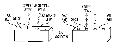
[0015] Figure 1 represents a printhead having printing orifices and a printing
face plate that are not modified. The accumulation of ink on the face plate of
the
printhead results in mis-directional jetting of the inkjet ink.
[0016] Figure 2 represents an alternate view of the printhead of
Figure 1.
[0017] Figure 3 represents a printhead before and after modification with a
SAM on the face plate of the printhead to prevent mis-directional jetting of
the inkjet
ink.
[0018] Figure 4 represents the difference in surface area energy between
unmodified and SAM modified printheads.
[0019] Figure 5 is an image of a 4x4 cm printed dots array with 100 pm
spacing printed with an inkjet printhead that is not modified.
[0020] Figure 6 is an image of a 4x4 cm printed dots array with 1001.1m
spacing printed using an inkjet printhead modified with a SAM.
[0021] Figures 7A and 7B illustrate deviation of a printed dots array from an
original pattern design, the extent of the deviation being measured as offset.
EMBODIMENTS
[0022] In embodiments, a printhead for inkjet printing includes a
modification of the printhead to have a self-assemble monolayer (SAM) thereon,
which prevents misdirectional jetting of the inkjet ink.
[0023] In embodiments, the inkjet printhead may be made from any effective
material, such as silicon, metals, ceramics, plastics or combinations thereof.
( . . . CA 02713810 2010-08-25
4
[0024] In further embodiments, the printhead is a piezoelectric printhead.
Exemplary printheads include the Spectra printhead, the Microfab printhead,
the Xaar
Printhead, the FujiFilm Dimatix piezoelectric printhead, the Xerox Solid ink
printhead, the Epson printhead and the like. Differently from conventional
printing,
in embodiments the SAM modified printhead is used in high precision material
deposition systems. Conventional printing, such as printing marks on paper,
can
tolerate an accuracy variability, or offset, between the original print
pattern and the
printed image of about 40 micrometers.
[0025] For printed electronic applications, an accuracy variability of below
about 10 gm, such as below about 5 Ign can be achieved. Such high accuracy is
required for applications such as printed electronics applications. In
embodiments, the
printhead has a nozzle or printing orifice with a diameter of no greater than
about
60 tim, such as less than about 45 tim, or less than about 30 Itm. The drop
size of an
ink droplet jetted from the printhead is small, for example not greater than
about
160 pL, such as less than about 50 pL, including less than about 35 pL or less
than
about 10 pL.
[0026] In embodiments, the misdirectional jetting of the inkjet ink may be
addressed by using a SAM that provides the surface of the inkjet printhead
(also
referred to as the nozzle plate) with a uniform surface energy around a
printing orifice
and provides the printing surface of the printhead with a physically smooth or
uniform
surface (that is, by covering any bumps or filling any concavities). It is
believed that
unifying the surface energy or physical texture of the printing surface around
the
printing orifice prevents ink buildup around the printing orifice, thereby
preventing
jetted ink from being drawn to the surface of the printhead or to ink on the
surface of
the printhead by eledtrostatic forces, physical interactions such as surface
tension, and
the like.
[0027] It is believed that a uniform surface energy and physical surface
smoothness can be achieved with a SAM surface layer because the SAM will
evenly
coat the printing surface of the printhead, covering any bumps or concavities
in the
printhead, and also presenting the same chemical groups across the printhead
without
substantial variation.
[0028] In embodiments, the self-assembly monolayer molecules comprise
amphiphilic molecules comprised of either: a) a hydrophobic domain which
f . . CA 02713810 2010-08-25
5
spontaneously associates with the surface from a polar solvent, and a
hydrophilic
domain which allows the molecules to be dispersed in the polar solvent and
which
remains associated with the polar phase after monolayer formation on the
surface, or
b) a hydrophilic domain which spontaneously associates with the surface from a
nonpolar solvent, and a hydrophobic domain which allows the molecules to be
dispersed in a nonpolar solvent and which remains associated with the nonpolar
phase
after monolayer formation on the surface.
[0029] By "amphiphilic" it is meant that the molecules have two or more
functional (and generally discrete) domains, defined herein as X and Y,
respectively,
each with corresponding and differing physical properties. Desirably, those
properties
are in the form of differing affinities for water, for example, water-soluble
and water-
insoluble groups. In turn, one or more first domains will have an increased
affinity
(for example, hydrophobic nature) for the surface or interface, while one or
more
second domains have an increased affinity (for example, hydrophilic nature)
for the
carrier solvent. The composition can be brought into sufficient proximity to a
suitable surface or interface (for example, liquid-liquid, liquid-air or
liquid-solid
interface), to permit the molecules to spontaneously orient themselves into
substantially monolayer form upon the surface of the printhead.
[0030] During and/or upon formation of the monolayer, latent reactive
groups, which are provided by either the surface (or at the interface with
another
phase) and/or the SAM-forming molecules themselves, can be activated in order
to
covalently attach the thus-formed monolayer to the surface or interface.
Embodiments, therefore, are not limited by the choice of SAM composition, or
by the
choice of surface/interface. Instead, a means that is generally applicable for
attaching
the monolayer to the corresponding inkjet printhead surface is provided.
[0031] In embodiments, the SAM is a hydrocarbon-containing layer formed
from a precursor. The precursor comprises a material having the following
formula:
X¨Y wherein X is a reactive group which can react with certain functional
group(s)
on the printhead surface, and Y is a hydrocarbon structure. In embodiments, X
is
selected from the groups consisting of ¨P03H3, ¨0P03H3, ¨COOH, ¨SiC13,
¨SiCl(CH3) 2, -SiC12CH3, -Si(OCH3)3, -SiC13, -Si(OC2115) 3, ¨OH, ¨SH,
¨CONHOH, ¨NCO, benzotriazolyl (¨C6H4N3), and the like. The hydrocarbon
structure in the hydrocarbon-containing layer may be a linear or branched
hydrocarbon
CA 02713810 2010-08-25
6
comprising the following exemplary number of carbon atoms: from 1 to about 60
carbon atoms, such as from about 3 to about 50 carbon atoms, from about 4 to
about
40 carbon atoms, from about 5 to about 30 carbon atoms, and/or from about 10
to
about 18 carbon atoms. In embodiments, the hydrocarbon structure is a linear
or
branched aliphatic or cyclic aliphatic group, a linear or branched group
containing an
aromatic group and/or aliphatic or cyclic aliphatic group, or an aromatic
group.
Reaction of the X group with the inkjet printhead surface will result in a
heteroatom
containing moiety in the substance, wherein the heteroatom containing moiety
is
covalently bonded to both the hydrocarbon structure and the inkjet printhead
surface.
Such a "heteroatom containing moiety" is not to be confused with the
"heteroatom-
containing group" of the "substituted hydrocarbon structure."
[0032] In embodiments, the precursor may be, for example, an alkylsilane,
alkylphosphine, alkyl halo silane or a mixture thereof, where the alkyl moiety
includes, for instance, from 1 to about 50 carbon atoms, from about 3 to about
50
carbon atoms, from about 4 to about 40 carbon atoms, from about 5 to about 30
carbon atoms, and/or from about 10 to about 18 carbon atoms. The halo in the
alkyl
halo silane may be chloro, fluoro, bromo and/or iodo.
[0033] In embodiments, the hydrocarbon structure may be a small molecule
structure or a polymeric structure. The hydrocarbon structure could be a
linear or
branched structure. The hydrocarbon structure could be aliphatic, cyclic
aliphatic,
aromatic structure, or mixture thereof. The phrase "hydrocarbon structure"
encompasses "substituted hydrocarbon structure" and "unsubstituted hydrocarbon
structure." In embodiments, the phrase "substituted hydrocarbon structure"
refers to
replacement of one or more hydrogen atoms of the organic compound/organic
moiety
with Cl, Br, I and a heteroatom-containing group such as for example CN, NO2,
amino group (NH2, NH), OH, COOH, alkoxyl group (0¨CH3), and the like, and
mixtures thereof. In embodiments, the phrase "unsubstituted hydrocarbon
structure"
indicates that the structure is absent any replacement of a hydrogen atom of
the
organic compound/organic moiety with a substituent described herein.
[0034] In embodiments, the SAM is a fluorocarbon-containing layer formed
from a precursor comprising SAM-forming molecules. The precursor comprises a
material having the following formula: X¨Y wherein X is a reactive group with
can
CA 02713810 2010-08-25
7
react with certain functional group(s) on the printhead surface, and Y is a
fluorocarbon
structure. In embodiments, X is selected from the groups consisting of ¨P03H3,
¨0P03H3, ¨COOH, ¨SiC13, ¨SiC1(CH3) 2, -SiC12CH3, -Si(OCH3)3, -SiC13,
-Si(0C2115) 3, ¨OH, ¨SH, ¨CONHOH, ¨NCO, benzotriazolyl (¨C6H4N3), and
the like. The fluorocarbon structure in the fluorocarbon-containing layer may
be a
linear or branched fluorinated hydrocarbon comprising the following exemplary
number of carbon atoms and fluorine atoms: 1 to about 60 carbon atoms, such as
from
about 3 to about 30 carbon atoms; and 1 to about 120 fluorine atoms, or from 2
to
about 60 fluorine atoms. In embodiments, the fluorocarbon structure in the
fluorocarbon-containing layer is a perfluorocarbon structure. In embodiments,
the
carbon atoms of the fluorocarbon structure in the fluorocarbon-containing
layer are
arranged in a chain of a length ranging for example from 3 to about 18 carbon
atoms.
In embodiments, the fluorocarbon structure may be a linear or branched
aliphatic or
cyclic aliphatic group, a linear or branched group containing an aromatic
group and/or
aliphatic or cyclic aliphatic group, or an aromatic group. Reaction of the X
group with
the inkjet printhead surface will result in a heteroatom containing moiety in
the
substance, wherein the heteroatom containing moiety is covalently bonded to
both the
fluorocarbon structure and the inkjet printhead surface. Such a "heteroatom
containing
moiety" is not to be confused with the "heteroatom-containing group" of the
"substituted fluorocarbon structure."
[0035] In embodiments, the phrase "fluorocarbon structure" refers to an
organic compound/organic moiety analogous to hydrocarbons in which one or more
hydrogen atoms has been replaced by fluorine. The fluorocarbon structure can
be a
small molecule structure or a polymeric structure. The fluorocarbon structure
may be a
linear or branched structure. The fluorocarbon structure could be aliphatic,
cyclic
aliphatic, aromatic structure, or mixture thereof. The phrase "fluorocarbon
structure"
encompasses "substituted fluorocarbon structure" and "unsubstituted
fluorocarbon
structure." In embodiments, the phrase "substituted fluorocarbon structure"
refers to
replacement of one or more hydrogen atoms of the fluorine-containing organic
compound/organic moiety with Cl, Br, I and a heteroatom-containing group such
as
for example CN, NO2, amino group (NH2, NH), OH, COOH, alkoxyl group
(0¨CH3), and the like, and mixtures thereof. In embodiments, the phrase
"unsubstituted fluorocarbon structure" indicates that there is absent any
replacement
CA 02713810 2010-08-25
8
of a hydrogen atom of the fluorine-containing organic compound/organic moiety
with
a substituent described herein.
100361 The precursor may be dispersed in a solvent before forming a layer
on the substrate. Exemplary solvents include aliphatic hydrocarbon, aromatic
hydrocarbon, alcohol, chlorinated solvent, ketone, ester, ether, amide, amine,
sulfone,
sulfoxide, carboxylic acid, tetrahydrofuran, heptane, octane, cyclohexane,
toluene,
xylene, mesitylene, dichloromethane, dichloroethane, chlorobenzene,
dichlorobenzene, nitrobenzene, propanols, butanols, pentanols,
dimethylsulfoxide,
dimethylformamide, alkanecarboxylic acids, arenecarboxylic acids, and mixtures
thereof.
100371 The carrier solvent (in which the SAM-forming molecules are
initially provided) and the surface to which the carrier solvent is applied
will
themselves typically have different affinities for water, corresponding to the
respective
domains of the SAM-forming molecules. In turn, when a composition of SAM-
forming molecules in carrier solvent is brought into physical proximity with
the
surface, or interface, the molecule domains spontaneously and preferentially
orient
themselves toward either the solvent or surface/interface, in order to form a
monolayer. The carrier solvent, in turn, is ideally one in which the second
domain of
the SAM-forming molecule has preferential solubility or affinity, and which
itself is
not a solvent for the surface.
[0038] The SAM precursor may be present in the solvent in a content of
from about 1 wt% to about 95 wt%, such as from about 5 wt% to about 90 wt%,
from
to about 80 wt%, or from about 25 wt% to about 75 wt%, by total weight of the
precursor and solvent.
[0039] The SAM precursor will be linked (usually covalently) to the
substrate through the reactive group X discussed above.
[0040] The inkjet printhead surface may directly link with the reactive group
X, or may react with X through a reactive coating on the inkjet printhead
surface, the
reactive coating including metals such as gold, mercury, ITO (indium-tin-
oxide),
siloxane and the like. The inkjet printhead surface may have a planar surface,
including compounds such as silicon, metals, plastics and the like, or curved
surfaces,
including compounds such as nanoparticles and the like.
CA 02713810 2010-08-25
9
[0041] In embodiments, the SAM may be formed from a trichlorosilane, or a
trichlorododecylsilane, monolayer. In embodiments, the SAM may be formed from
a
fluorotrichlorosilane, or a fluorotrichlorododecylsilane, monolayer. In
embodiments,
the SAM may be a siloxane monolayer.
[0042] In embodiments, the SAM is a single layer. In other embodiments,
there is present a plurality of two or more SAM layers. In embodiments, the
layer
material is a polymer (having a degree of polymerization "n" of about 2 or
more such,
as for example, from about 2 to about 100).
[0043] A single SAM layer typically has a thickness of less than about 5
nanometers, such as less than about 2 nanometers. In embodiments, the layer is
a
crosslinked layer, such as through siloxane bonds formed between adjacent
silicon
groups of the monolayer constituents. In embodiments, the layer material is
covalently bonded to the printhead. In other embodiments, the layer material
is not
covalently bonded to the printhead.
[0044] Also disclosed is a method for forming a self-assembly monolayer on
a printhead surface, the method comprising the steps of: a) providing on the
surface
both latent reactive groups and a monolayer formed of self-assembling
monolayer
, molecules, and b) activating the latent reactive groups under conditions
suitable to
either covalently attach the self-assembled monolayer to the surface and/or to
form a
stable monolayer film on the surface, for example by initiating polymerization
of
suitable groups provided by self-assembling monolayer molecules themselves
and/or
by forming intermolecular bonds between the self-assembling monolayer
molecules.
[0045] The SAM layer may be deposited on the printhead substrate by any
known or effective technique, such as formation of a SAM layer from a
precursor in
solution or using physical vapor deposition, electrodeposition, electroless
deposition,
and the like.
[0046] Physical vapor deposition techniques include evaporative deposition,
in which the material to be deposited is heated to a high vapor pressure by
electrically
resistive heating in low vacuum; electron beam physical vapor deposition, in
which
the material to be deposited is heated to a high vapor pressure by electron
bombardment in high vacuum; sputter deposition, in which a glow plasma
discharge
bombards the material, thereby sputtering some away as a vapor; cathodic arc
deposition, in which a high power arc directed at the target material blasts
away some
CA 02713810 2012-05-14
into a vapor; pulsed laser deposition, in which a high power laser ablates
material
from the target into a vapor; and the like.
[0047] The process for modifying an inkjet printhead may include, for
example, immersing the printhead in a SAM precursor solution in toluene to
grow a
SAM layer on the printhead. After immersion, the printhead may be rinsed with
toluene.
[0048] The concentration of the SAM precursor solution (concentration of
the SAM-forming material in solution) may be from about 0.001 M to about 1 M,
such as from about 0.01 M to about 0.2 M. In embodiments, the concentration of
the
SAM precursor solution may be about 0.1 M. The printhead may be immersed in
the
SAM precursor solution from about 1 min to about 1 hour, including from about
5
min to about 30 min at a suitable temperature such as from about room
temperature
(such as from about 20 C to about 25 C) to 100 C, including from room
temperature
to about 60 C. In embodiments, the printhead is modified using a SAM precursor
solution concentration of about 0.1 M at 60 C for 20 mm.
[0049] SAMs can be prepared using various methods, such as the Langmuir
Blodgett technique, which involves the transfer of a film pre-assembled at an
air water
interface to a solid substrate. SAMs can also be prepared by a self-assembly
process
that occurs spontaneously upon immersion of the inkjet printhead into a
solution
containing an appropriate amphiphile or a solution of solvent and amphiphilic
compound precursors.
[0050] The process for modifying an inkjet printhead may also include an
initial preparation step such as cleaning the printhead in an acid bath or
using a plasma
cleaning method to clean the printhead before applying the SAM to the printing
surface of the printhead.
[0051] In embodiments, the SAM layer is applied to the printing plate
surface of the inkjet printhead, around the printing orifice of the inkjet
printhead, or
over the entirety of the inkjet printhead, including inside the printing
orifice.
Particularly beneficial inkjet accuracy and detailed droplet control may be
achieved
when the SAM layer is applied over the entirety of the inkjet printhead,
including
inside the printing orifice, for printing of electronic materials inks.
100521 Prior to SAM modification, the surface of printhead has a variable
surface energy which can be measured using advancing water contact angle
CA 02713810 2010-08-25
11
measurement techniques. Prior to modification, the surface of the printhead
has a
high surface energy with a water contact angle as measured at room temperature
of
from about 20 degrees to about 80 degrees, such as from about 30 degrees to
about 75
degrees. Moreover, if positions are measured on a printhead surface that has
not been
SAM modified, the variation of water contact angles between measurement
positions
on the printhead surface is large, such as larger than about 8 degrees, larger
than about
15 degrees, or larger than about 20 degrees. After modification of the
printhead with
a SAM layer, the surface of the printhead has a low surface energy, exhibiting
a water
contact angle of from about 90 degrees to about 120 degrees, such as from
about 95
degrees to about 105 degrees. Additionally, the surface energy of the
printhead
printing surface is substantially uniform. For example, the variation of water
contact
angle between two or more measurement positions on the SAM modified printhead
is
less than about 8 degrees, such as less than about 5 degrees or less than
about 3
degrees, from position to position on the printhead surface.
[0053] The surface-modified inkjet printhead may be used to print any type
of inkjet ink or jettable composition onto any appropriate substrate such as
glass,
polyethylene terephtalate (PET), PEN, polyimide, and the like, utilizing
application
techniques such as drop-on-demand inkjet printing or intermediate printing.
Products
produced using the disclosed printhead can include, but are not limited to,
electronic
devices, photovoltaic devices, organic light emitting diode (OLED) devices,
thin film
transistors (TFT), microfluid devices, and the like.
[0054] Also disclosed is a process for producing printed electronics
comprising the step of printing an electronic material in the form of an
inkjet ink or
jettable composition onto a substrate using an inkjet printhead modified to
include a
surface layer, such as a SAM, on the printing surface of an inkjet printhead.
[0055] The printed electronic materials may be semiconductor materials
including organic semiconductor materials, conductor materials such as silver
nanoparticle inks, insulating materials, and the like.
[0056] The printed electronics material ink may be an ink composed of
electronic materials in a solvent. Exemplary electronic materials include
polythiophene, oligothiophene, pentacene precursors or thiophene-arylene
copolymer.
In embodiments, the electronic material comprises
CA 02713810 2010-08-25
12
poly( 3,3"-didodecylquarterthiophene) (PQT) nanoparticles. Exemplary solvents
include aliphatic hydrocarbon, aromatic hydrocarbon, alcohol, chlorinated
solvent,
ketone, ester, ether, amide, amine, sulfone, sulfoxide, carboxylic acid,
tetrahydrofuran,
heptane, octane, cyclohexane, toluene, xylene, mesitylene, dichloromethane,
dichloroethane, chlorobenzene, dichlorobenzene, nitrobenzene, propanols,
butanols,
pentanols, dimethylsulfoxide, dimethylformamide, alkanecarboxylic acids,
arenecarboxylic acids, heir derivatives, or mixtures thereof The solvent may
be a
1,2- dichlorobenzene.
[0057] In further embodiments, the electronic material has a low surface
tension such as less than about 35 mN/m, less than about 30 mN/m, or less than
about
26 mN/m. In embodiments, the electronic material is a Newtonian fluid. In
embodiments, the electronic material is a non-Newtonian fluid such as a fluid
having
a gel structure or a fluid comprising nanoparticles. The electronic material
may have a
viscosity less than about 10 cps, or less than about 5 cps at a high shear
rate such as
1000 s-1. In embodiments, the SAM modified printhead is used for printing of
non-Newtonian fluids with low surface tensions and low viscosities, or
non-Newtonian fluids having a gel structure or comprising nanoparticles.
[0058] Figure 1 shows an inkjet printhead having printing orifices and a
printing plate that are not modified. Ink is shown accumulated around a
printing
orifice, thereby causing misdirectional jetting of later jetted ink. When the
ink is not
present around the printing orifice, misdirected jetting of ink is not
observed.
[0059] Figure 2 shows an inkjet printhead having printing orifices and a
printing plate that are not modified. Variations in surface energy of the
printing
surface of the printhead, particularly surface energy variations around a
printing
orifice are another source of misdirectional jetting of ink droplets. When the
surface
energy is uniform around the printing orifice of the printhead, the ink
droplets are not
drawn or pushed from their intended delivery path, and thereby create a more
controlled and accurate deposition on the desired substrate.
[0060] Figure 3 shows that incorporation of a SAM layer onto inkjet
printhead can reduce accumulation of ink around the printing orifice, and
thereby
decrease undesirable misdirectional jetting of ink.
CA 02713810 2010-08-25
13
[0061] Figure 4 shows that incorporation of a SAM layer onto an inkjet
printhead can reduce variation in surface energy of the printhead around the
printing
orifice, and reduce misdirectional jetting of ink in this manner as well.
[0062] Figure 5 is an image of the results of the Comparative Example, a
4x4 cm dots array printed with 100 um spacing, printed using a standard (no
SAM
layer modification) inkjet printhead to evaluate printing accuracy. As can be
seen, a
large percentage of printed dots were not printed accurately, showing the
results of
misdirectional printing.
[0063] Figure 6 is an image of the results of the Example. Figure 6 is an
image of another 4x4 cam dots array printed with 100 gm spacing, printed with
an
inkjet printhead modified with a SAM layer. It is clearly evident that
significantly
improved accuracy was achieved using the SAM-modified inkjet printhead as
compared to the non-modified inkjet printhead of the Comparative Example.
An offset value is used to illustrate the printing accuracy. The drop offset
is the
distance differentiation between the printed image and the original image
design. As
shown in Figures 7A and 7B, printed dots may deviate from the original image
design.
The difference (offset) between the printed image and the original image
design can
be measured. In embodiments, the offset is less than about 30 urn, such as
less than
about 20 urn, or less than about 10 urn, in both the x and y directions.
[0064] The following examples were prepared to further illustrate
embodiments described herein.
COMPARATIVE EXAMPLE
[0065] An ink composed of PQT nanoparticles in 1,2-dichlorobenzene was
printed using a Dimatix inkjet printer equipped with a 10 pL cartridge to
deposit the
ink on a substrate in a 4x4 cm dots array with 100 gm spacing to ascertain
printing
accuracy. The results of the printing test are shown in Figure 5. Most rows
showed
misdirectional deposition of the ink on the substrate.
EXAMPLE
[0066] Prior to printing a dots array as in the comparative example, the
printhead was first immersed in a 0.1 M trichlorododecylsilane solution in
toluene at
room temperature for 30 minutes to grow a SAM on the surface of the printhead
face
plate. After modification, the printhead was rinsed with toluene thoroughly
and dried.
The same 4x4 cm dots array as in the comparative example was printed. The
results
CA 02713810 2010-08-25
14
of the printing test may be seen in Figure 6. No misfiring drops were observed
in the
printed dots array.
[0067] It will be appreciated that various of the above-disclosed and other
features and functions, or alternatives thereof, may be desirably combined
into many
other different systems or applications. Also, various presently unforeseen or
unanticipated alternatives, modifications, variations or improvements therein
may be
subsequently made by those skilled in the art, and are also intended to be
encompassed by the following claims.