Language selection

Search

Patent 2714810 Summary

Third-party information liability

Some of the information on this Web page has been provided by external sources. The Government of Canada is not responsible for the accuracy, reliability or currency of the information supplied by external sources. Users wishing to rely upon this information should consult directly with the source of the information. Content provided by external sources is not subject to official languages, privacy and accessibility requirements.

Claims and Abstract availability

Any discrepancies in the text and image of the Claims and Abstract are due to differing posting times. Text of the Claims and Abstract are posted:

  • At the time the application is open to public inspection;
  • At the time of issue of the patent (grant).
(12) Patent Application: (11) CA 2714810
(54) English Title: PHOTOVOLTAIC MODULE
(54) French Title: MODULE PHOTOVOLTAIQUE
Status: Deemed Abandoned and Beyond the Period of Reinstatement - Pending Response to Notice of Disregarded Communication
Bibliographic Data
(51) International Patent Classification (IPC):
  • H01L 31/048 (2014.01)
(72) Inventors :
  • EUSCH, INGRAM (Austria)
  • FRANK, RUDOLF (Austria)
  • KOGLER, ARMIN (Austria)
(73) Owners :
  • KIOTO PHOTOVOLTAICS GMBH
(71) Applicants :
  • KIOTO PHOTOVOLTAICS GMBH (Austria)
(74) Agent: NORTON ROSE FULBRIGHT CANADA LLP/S.E.N.C.R.L., S.R.L.
(74) Associate agent:
(45) Issued:
(22) Filed Date: 2010-09-14
(41) Open to Public Inspection: 2011-06-17
Examination requested: 2011-02-11
Availability of licence: N/A
Dedicated to the Public: N/A
(25) Language of filing: English

Patent Cooperation Treaty (PCT): No

(30) Application Priority Data:
Application No. Country/Territory Date
09 015 596.1 (European Patent Office (EPO)) 2009-12-17

Abstracts

English Abstract


The invention concerns a photovoltaic module with a transparent cover,
that forms a first main surface of the module, a protective layer, that
runs parallel and with a distance to the cover and forms a second main
surface of the module, a first adhesive layer between the cover and a
photovoltaic layer formed from a multitude of cells, a second adhesive
layer between the protective layer and the photovoltaic layer, wherein
the first and second adhesive layer are extending into an area between
the cells of the photovoltaic layer and around the cells and are projecting
the module circumferentially at the edge by 0,1 to 3 mm.


Claims

Note: Claims are shown in the official language in which they were submitted.

-8-
claims
1. The photovoltaic module with
1.1 a transparent cover (10), that forms a first main surface of the
module,
1.2 a protective layer (18), that runs parallel and with a distance to
the cover (10) and forms a second main surface of the module,
1.3 a first adhesive layer (12) between the cover (10) and a
photovoltaic layer formed from a multitude of cells (14),
1.4 a second adhesive layer (16) between the protective layer (18)
and the photovoltaic layer, wherein
1.5 the first and second adhesive layer (12, 16) extend into an area
(20) between the cells (14) of the photovoltaic layer and
around the cells (14) and are projecting the module
circumferentially at its edge by 0,1. - 3 mm.
2. The photovoltaic module according to claim 1, wherein at least the
first adhesive layer (12) extends continuously until projecting
corresponding edge areas (10r) of the cover (10).
3. The photovoltaic module according to claim 1, wherein the first
and the second adhesive layer (12, 16) are circumferentially
projecting the module at its edge by not more than 1 mm.
4. The photovoltaic module according to claim 1, wherein the first
and the second adhesive layer (12, 16) are circumferentially
projecting the module at its edge by not more than 0,2 mm.

-9-
5. The photovoltaic module according to claim 1, wherein at least
one adhesive layer (12, 16) is formed from an adhesive foil.
6. The photovoltaic module according to claim 5, wherein at least
one adhesive foil (12, 16) consists of cross-linked ethylene-vinyl-
acetate.
7. The photovoltaic module according to claim 1, wherein at least
one adhesive layer (12, 16) has a thickness, perpendicular to the
cover (10), of 0,1 to 1,0 mm.
8. The photovoltaic module according to claim 1, wherein the
protective layer (18) has a thickness, perpendicular to the cover
(10), of 0,1 to 1,0 mm.
9. The photovoltaic module according to claim 1, wherein the
protective layer (18) is made of a composite foil.
10. The photovoltaic module according to claim 1, wherein the cover
(10) is made of glass.
11. The photovoltaic module according to claim 1, wherein the cover
(10) has at least three markings (22) at a defined distance to each
other.
12. The photovoltaic module according to claim 1, wherein the cover
(10) has four markings (22), which form the corners of a fictitious
rectangle.

Description

Note: Descriptions are shown in the official language in which they were submitted.


CA 02714810 2010-09-14
photovoltaic module
description
The invention concerns a photovoltaic module. Main components of such
a solar module with solar cells from crystalline silicon are. a, transparent
cover, foils in which the solar cells with their associated electrical
contacting and electrical terminal elements are embedded and a
protective layer opposing the cover also called back sheet.
It is known to arrange the cover, the foils (adhesive layers) with
intermediate. photovoltaic cells .and the protective layer o.n top of each
other to be combined to a compact cavity free unit, the photovoltaic
module, in a vacuum, laminating process. Because of the heating. during
the lamination process (for example 200 C) said foils turn viscous, fill
the cavities between and around the photovoltaic cells and
simultaneously form the desired adhesive joint between cover and
photovoltaic layer and photovoltaic layer and protective layer
respectively.

CA 02714810 2010-09-14
-2-
After the lamination process the parts of the foil. and the.protective layer
protruding laterally (protruding parts of the adhesive layer) are being cut
off exactly to the design of the transparent cover. For this purpose. a
knife is guided along the edge of the cover.
This procedure has various disadvantages:
During the cutting off of protruding parts of the foil/adhesive
layer/protective layer the cover can be damaged at its edge. By this
damage undesirable wedges are formed between the individual layers of
the module in which afterwards moisture can intrude, which is
particularly problematic in freeze-/thaw-cycles.
Such wedges may also form in transition regions between the individual
layers laterally. The aforesaid problems emerge analogously..
The transparent cover, usually made of glass, is regularly not exactly
rectangular. While two opposing side edges are usually parallel this is
often not true for the connecting side edges. Often there is a trapezoid
geometry or a rhombus basic form.
Both causes problems, when the photovoltaic.module is afterwards
inserted into the according frame which is exactly rectangular. Usually a
reliable sealing cannot be achieved in that case.
One object of the invention it to avoid the aforesaid disadvantages.

CA 02714810 2010-09-14
-3-
The basic idea of the invention is the understanding. that an essential
problem is that irregularities (di.scontinuities) up to holes or cavities in
the edge area of the module are responsible for the problems outlined.
These irregularities can be removed after the lamination process and the
cutting by a separate processing step, for example by a. subsequent
sealing. The additional processing step would not only extend the
manufacturing time but also cause additional costs.
The essential idea of the invention is therefore to use the foils (adhesive
layers themselves) for sealing the edge of the module.
As disclosed the foils (adhesive foils) melt during the lamination
process, turn viscous and then fill for example sections between adjacent
photovoltaic cells and/or sections around the photovoltaic cells as well
as any other cavities. In this process a part of the material flows
inevitably also over the circumference marginal area and then further
along the marginal area in particularly of the transparent cover.
In other words: a circumferential coating from the material of the
adhesive layer is formed in-situ, that is not only protecting the marginal
area of the cover but also covers connection areas to the cover and the
protective layer respectively. A virtually monolithic circumferential
(along. its, edge) coating is formed that is starting from a section, between
protective layer and

CA 02714810 2010-09-14
-4-
cover that is running along the edge and is circumferentially projecting
beyond the cover.
The subsequent cutting is done in such a way that the adhesive layer is
circumferentially projecting, the module at its edge only by 0,1 to 3 mm.
In other words: contrary to the state of the art the projecting sections of
the adhesive layer and/or the protective layer are not being flush-cut to
the overall dimensions of the cover, but a projecting edge of adhesive
layer(s) and possibly of the protective layer remains.
This projection protects the cover at its edge as well as any terminal
areas of the cover and/or protective layer to adjacent parts of the
photovoltaic module reliably.
At the same time the cutting can take place in such a way that the
finished module has an exactly rectangular form not dependent on said
tolerances of the cover.
It is known that the cover can for example exhibit dimensional tolerances
from +/- 1,5 mm at, a basic dimension of 985 x 1,500 mm with regard to
length and width (or +/- 3,2 mm diagonally). From this a tolerance factor
can be calculated that can be improved by cutting according to the
invention by at least 50 %, but also by at least .90 % that is with regard
to tolerances according to the basic dimension of for example +/- 0,2 mm
(length, width).
The respective cutting is facilitated if the cover shows at least three, for
a rectangular cover usually four defined markings that are optically
detected before cutting to allow a rectangular cutting to the greatest
possible extent.

CA 02714810 2010-09-14
-5-
These markings can be dots, crosses or angles in, the corner region of the
cover and remain there, that is why they should be designed
inconspicuously in their size and color.
According to one embodiment the first adhesive layer extends
continuously until projecting corresponding edge .sections of the cover.
This may apply analogously for the second adhesive layer.
According to one embodiment the circumferential projection at the edge
is not more `than 1 mm and according to another embodiment at least -0,2
mm.
As already mentioned the adhesive layer may be formed: from an
adhesive foil for example from cross-linked ethylene-vinyl-acetate
(EVA). Such foils or adhesive layers are state of the art for solar
modules.
This also applies for the protective layer (back sheet) for a composite
foil for example on the basis of polyvinylfluoride (PVF)..Such a foil has
a relatively high stability and reflectivity. It is at the same time
weatherproof and UV-resistant.
Whereas the foils or the adhesive layers formed: thereof usually have a
thickness, perpendicularly to the cover, of 0,1 to 1,0 mm, and this also
applies far the thickness of the protective layer, a material thickness of
0,2 to 0,8 mm for the adhesive foils and from 0,2 to 0,7 mm for the
protective foil has proved adequate wherein the photovoltaic cells
usually have a thickness of up to 0,2 mm, so that with said foil
thicknesses it is ensured that- these can also fill cavities between and
adjacent to the cells during the lamination process.

CA 02714810 2010-09-14
-6-
Other features of the inventions arise from the features of the sub claims
as well as the other application documents.
The invention is described in more detail below with one embodiment.
This shows each in a simplified representation -
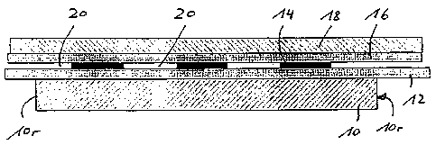
Figure 1: the arrangement of cover, foils and protective layer as well
as photovoltaic cells prior to the lamination process.
Figure 2: the arrangement of cover, foils and. protective layer as well
as photovoltaic cells after the lamination process.
Figure 3: a top view on the module according to figure 2 (from below).
In the figures components which are similar or with similar effects are
represented with identical characters.
The production of a photovoltaic module is done as .follows:
On top of a transparent cover 10, here: made of glass, an EVA-foil 12 is
placed, on top of the EVA-foil 12 photovoltaic cells 14 are placed
(which are each interconnected to a string) there on top again a second
EVA-foil 16 and finally there on top a protective layer 18 made of
polyvinylfluorid.e.
Figure 1 shows that the foils 12, 16 as well as the protective layer 18 are
projecting the cover 10 (on all sides) at its edge. Figure 1 also shows
that between adjacent cells 14 or around the cells 14 respectively
sections 20 are present that form cavities.
Within a vacuum lamination line foils 12, 16 turn viscous at approximately
150 C and flow into the section 20 and over the peripheral region I Or

CA 02714810 2010-09-14
-7-
of the cover 10. The foil material cures as soon as the maximum
temperature within the lamination line is set back to ambient
temperatures.
In a subsequent cutting station the dimensioning of photovoltaic module
takes place in such a way that the adhesive layers, that are made up of
the foils 12, 16, are slightly projecting the edge l Or of the cover 10, in
this case: about 0,2 mm as schematically represented in figure 2.
The photovoltaic module shown in a vertical cross section in figure 2 has
a more or less exact outer rectangular geometry as results from the top
view according to figure 3, wherein the cover 10 itself has
(exaggeratedly shown in figure 3) a trapezoidal design which was
compensated by cutting off the projections of foils 12, 16 and the
protective layer 18 accordingly.
For this purpose the cover 10 made of glass has four cross-shaped labels
22 in the corner region of the cover 10, wherein these labels 22 define
the position. of the cover 10 in the cutting station so that it can
subsequently be cut-to size exactly..
From the trapezoidal geometry of the cover 10 it results inevitably that
the projection 12u of the adhesive layer 12 (adhesive foil .12) is not
equal on all sides. This is not only accepted but explicitly desired, so
that the module obtains an overall rectangular form and can then be
mounted
.,fitting exactly in an according frame.

Representative Drawing
A single figure which represents the drawing illustrating the invention.
Administrative Status

2024-08-01:As part of the Next Generation Patents (NGP) transition, the Canadian Patents Database (CPD) now contains a more detailed Event History, which replicates the Event Log of our new back-office solution.

Please note that "Inactive:" events refers to events no longer in use in our new back-office solution.

For a clearer understanding of the status of the application/patent presented on this page, the site Disclaimer , as well as the definitions for Patent , Event History , Maintenance Fee  and Payment History  should be consulted.

Event History

Description Date
Inactive: Dead - Final fee not paid 2014-07-10
Application Not Reinstated by Deadline 2014-07-10
Inactive: IPC removed 2014-05-22
Inactive: First IPC assigned 2014-05-22
Inactive: IPC assigned 2014-05-22
Inactive: IPC expired 2014-01-01
Inactive: IPC removed 2013-12-31
Deemed Abandoned - Failure to Respond to Maintenance Fee Notice 2013-09-16
Deemed Abandoned - Conditions for Grant Determined Not Compliant 2013-07-10
Notice of Allowance is Issued 2013-01-10
Letter Sent 2013-01-10
Notice of Allowance is Issued 2013-01-10
Inactive: Approved for allowance (AFA) 2012-12-05
Application Published (Open to Public Inspection) 2011-06-17
Inactive: Cover page published 2011-06-16
Letter Sent 2011-02-23
Inactive: Office letter 2011-02-22
Request for Examination Requirements Determined Compliant 2011-02-11
All Requirements for Examination Determined Compliant 2011-02-11
Request for Examination Received 2011-02-11
Inactive: Correspondence - Formalities 2011-01-26
Inactive: IPC assigned 2010-10-21
Inactive: First IPC assigned 2010-10-21
Inactive: IPC assigned 2010-10-21
Inactive: Filing certificate - No RFE (English) 2010-10-05
Filing Requirements Determined Compliant 2010-10-05
Letter Sent 2010-10-05
Application Received - Regular National 2010-10-05

Abandonment History

Abandonment Date Reason Reinstatement Date
2013-09-16
2013-07-10

Maintenance Fee

The last payment was received on 2012-09-05

Note : If the full payment has not been received on or before the date indicated, a further fee may be required which may be one of the following

  • the reinstatement fee;
  • the late payment fee; or
  • additional fee to reverse deemed expiry.

Please refer to the CIPO Patent Fees web page to see all current fee amounts.

Fee History

Fee Type Anniversary Year Due Date Paid Date
Application fee - standard 2010-09-14
Registration of a document 2010-09-14
Request for examination - standard 2011-02-11
MF (application, 2nd anniv.) - standard 02 2012-09-14 2012-09-05
Owners on Record

Note: Records showing the ownership history in alphabetical order.

Current Owners on Record
KIOTO PHOTOVOLTAICS GMBH
Past Owners on Record
ARMIN KOGLER
INGRAM EUSCH
RUDOLF FRANK
Past Owners that do not appear in the "Owners on Record" listing will appear in other documentation within the application.
Documents

To view selected files, please enter reCAPTCHA code :


To view images, click a link in the Document Description column. To download the documents, select one or more checkboxes in the first column and then click the "Download Selected in PDF format (Zip Archive)" or the "Download Selected as Single PDF" button.

List of published and non-published patent-specific documents on the CPD .

If you have any difficulty accessing content, you can call the Client Service Centre at 1-866-997-1936 or send them an e-mail at CIPO Client Service Centre.


Document
Description 
Date
(yyyy-mm-dd) 
Number of pages   Size of Image (KB) 
Claims 2010-09-14 2 66
Drawings 2010-09-14 1 106
Description 2010-09-14 7 275
Abstract 2010-09-14 1 20
Representative drawing 2011-05-20 1 46
Cover Page 2011-06-13 1 74
Courtesy - Certificate of registration (related document(s)) 2010-10-05 1 103
Filing Certificate (English) 2010-10-05 1 155
Acknowledgement of Request for Examination 2011-02-23 1 176
Reminder of maintenance fee due 2012-05-15 1 112
Commissioner's Notice - Application Found Allowable 2013-01-10 1 162
Courtesy - Abandonment Letter (NOA) 2013-09-04 1 164
Courtesy - Abandonment Letter (Maintenance Fee) 2013-11-12 1 172
Correspondence 2011-01-26 3 106
Correspondence 2011-02-22 1 13