Note: Descriptions are shown in the official language in which they were submitted.
307/1053PC PF 60561 CA 02715040 2010-08-05
1
As originally filed
Doped tin tellurides for thermoelectric applications
Description
The present invention relates to semiconductor materials comprising tin and
generally
tellurium, and also at least one or two further dopants, and to thermoelectric
generators
and Peltier arrangements comprising said materials.
Thermoelectric generators and Peltier arrangements as such have been known for
some time. p- and n-doped semiconductors which are heated on one side and
cooled
on the other side transport electrical charges through an external circuit,
and electrical
work can be performed by a load in the circuit. The efficiency of conversion
of heat to
electrical energy achieved in this process is limited thermodynamically by the
Carnot
efficiency. Thus, at a temperature of 1000 K on the hot side and 400 K on the
"cold"
side, an efficiency of (1000 - 400) : 1000 = 60% would be possible. However,
only
efficiencies of up to 10% have been achieved to date.
On the other hand, when a direct current is applied to such an arrangement,
heat is
transported from one side to the other side. Such a Peltier arrangement works
as a
heat pump and is therefore suitable for cooling apparatus parts, vehicles or
buildings.
Heating via the Peltier principle is also more favorable than conventional
heating,
because more heat is always transported than corresponds to the energy
equivalent
supplied.
A good review of effects and materials is given, for example, by Cronin B.
Vining, ITS
Short Course on Thermoelectricity, Nov. 8, 1993, Yokohama, Japan.
At present, thermoelectric generators are used, for example, in space probes
for
generating direct currents, for cathodic corrosion protection of pipelines,
for energy
supply to light buoys and radio buoys and for operating radios and television
sets. The
advantages cf thermoelectric generators lie in their extreme reliability. For
instance,
they work irrespective of atmospheric conditions such as atmospheric moisture;
there
is no fault-prone mass transfer, but rather only charge transfer. It is
possible to use any
fuels from hydrogen through natural gas, gasoline, kerosene, diesel fuel up to
biologically obtained fuels such as rapeseed oil methyl ester.
Thermoelectric energy conversion thus fits extremely flexibly into future
requirements
B07/10533 FIC PF 6056 CA 02715040 2010-08-05
2
such as hydrogen economy or energy generation fi-om renewable energies.
A particularly attractive application is the use for converting (waste) heat
to electrical
energy in motor vehicles, heating systems or power plants. Thermal energy
unutilized
to date can even now by recovered at least partly by thermoelectric
generators, but
existing technologies achieve efficiencies of significantly below 10%, and so
a large
part of the energy is still lost unutilized. In the utilization of waste heat,
there is
therefore also a drive toward significantly higher efficiencies.
The conversion of solar energy directly to electrical energy would also be
very
attractive. Concentrators such as parabolic troughs can concentrate solar
energy into
thermoelectric generators, which generates electrical energy.
However, higher efficiencies are also needed for use as a heat pump.
Thermoelectrically active materials are rated essentially with reference to
their
efficiency. A characteristic of thermoelectric materials in this regard is
what is known as
the Z factor (figure of merit):
Z
X
with the Seebeck coefficient S, the electrical conductivity a and the thermal
conductivity
K. Preference is given to thermoelectric materials which have a very low
thermal
conductivity, a very high electrical conductivity and a very large Seebeck
coefficient,
such that the figure of merit assumes a maximum value.
The product Sea is referred to as the power factor and serves for comparison
of the
thermoelectric materials.
In addition, the dimensionless product Z = T is often also reported for
comparative
purposes. Thermoelectric materials known hitherto have maximum values of Z T
of
about 1 at an optimal temperature. Beyond this optimal temperature, the values
of Z a T
are often significantly lower than 1.
A more precise analysis shows that the efficiency q is calculated from
CA 02715040 2010-08-05
77 =
where
ELI-
I+ Z (1,,;,,,, + T,,,,,,
(see also Mat. Sci. and Eng. B29 (1995) 228).
The aim is thus to provide a thermoelectric material having a maximum value of
Z and
a high realizable temperature differential. From the point of view of solid
state physics,
many problems have to be overcome here:
A high a requires a high electron mobility in the material, i.e. electrons (or
holes in p-
conducting materials) must not be bound strongly to the atomic cores.
Materials having
high electrical conductivity o usually simultaneously have a high thermal
conductivity
(Wiedemann - Franz law), which does not allow Z to be favorably influenced.
Materials
used at present, such as Bi2Te3, already constitute compromises. For instance,
the
electrical conductivity is lowered to a lesser extent by alloying than the
thermal
conductivity. Preference is therefore given to using alloys, for example
(Bi2Te3)90(Sb2Te3)5(Sb2Se3)5 Or Bi12Sb23Te65, as described in US 5,448,109.
For thermoelectric materials having high efficiency, still further boundary
conditions
preferably have to be fulfilled. For instance, they have to be sufficiently
thermally stable
to be able to work under operating conditions over the course of years without
significant loss of efficiency. This requires a phase which is thermally
stable at high
temperatures per se, a stable phase composition, and negligible diffusion of
alloy
constituents into the adjoining contact materials.
Doped lead tellurides for thermoelectric applications are described, for
example, in WO
2007/104601. These are lead tellurides which, as well as a majority of lead,
also
comprise one or two further dopants. The particular proportion of the dopants,
based
on the formula (I) specified in the WO, is from 1 ppm to 0.05. Example 5
discloses
Pb0.937Ge0.01Sn0.0o3Te1.o01. This material actually includes the lowest lead
content of the
illustrative compounds. The materials thus have very high lead contents and
only very
low tin contents, if any.
WO 2007/104603 relates to lead germanium tellurides for thermoelectric
applications.
CA 02715040 2010-08-05
4
These are ternary compounds of lead, germanium and tellurium, in which very
high
lead contents are again present.
For the production of a thermoelectric module, n- and p-conductors are always
necessary. In order to arrive at a maximum efficiency of the module, i.e. at a
maximum
cooling performance in the case of a Peltier arrangement or a maximum
generator
performance in the case of a Seebeck arrangement, p-conductive and n-
conductive
material must be as well matched to one another as possible. This relates in
particular
to the parameters of Seebeck coefficient (ideally S(n) = -S(p)), electrical
conductivity
(ideally a(n) = 6(p)), thermal conductivity (ideally n,(n) = ?gy(p)) and
coefficient of thermal
expansion (ideally a(n) = a(p)).
Proceeding from this prior art and the material requirements mentioned, it is
an object
of the present invention to provide thermoelectrically active materials which
have a
high thermoelectric efficiency and exhibit a suitable profile of properties
for different
application sectors. They should preferably include materials which, within
the
temperature range under application conditions (typically between ambient
temperature
and at least 150 C), do not undergo any change in the mechanism of conduction.
The object is achieved in accordance with the invention by a
p- or n-conductive semiconductor material comprising a compound of the general
formula (I)
Sna Pb1-a-(x1+...+xn) A1x1...Anxn (Tet-P-g-r SepSgXr)1+z (1)
where
0.05 < a < 1
n > 1 where n is the number of chemical elements different than Sn and Pb
in each case independently
1 ppm <- x1 ... xn s 0.05
A' ... An are different from one another and are selected from the group of
the
elements Li, Na, K, Rb, Cs, Mg, Ca, Y, Ti, Zr, Hf, Nb, Ta, Cr, Mn, Fe, Cu, Ag,
Au,
Ga, In, TI, Ge, Sb, Bi
- 3 /10 5 PC ice:' :50 5 31. CA 02715040 2010-08-05
- 9
X is F, Cl, Br or 1
0<<<p<<<1
5 0q<_1
0r<0.01
- 0.01 <_z<_0.01
with the condition that p + q + r<_ 1 and a + x1 + ... + xn <_ 1.
It has been found in accordance with the invention that tin tellurides with a
tin content
of more than 5% by weight, preferably of at least 10% by weight, especially of
at least
20% by weight, have very good thermoelectric properties when they are admixed
with
at least one additional dopant.
it has additionally been found in accordance with the invention that a change
in the
mechanism of conduction, for example from p-conduction to n-conduction with
rising
temperature in the Sn-rich materials, was suppressible. This change is
frequently a
problem in the Pb-rich systems, since the p-conductive samples, in spite of
good start
values at room temperature, switch reversibly to the n-conductive region at no
higher
than 300 C and are therefore not useful for an application at higher
temperatures. This
problem can be avoided by using the inventive Sn-rich materials.
In the compounds of the general formula (1), n indicates the number of
chemical
elements different than SnPb, not including Te, Se, S and X. The materials may
be
pure tellurides. In this case, p = q = r = 0. Tellurium may also be replaced
partly or
completely by selenium, sulfur or, in small amounts, halide. Preferably 0 <_ p
< 0.2,
more preferably 0 <_ p <_ 0.05. Preferably 0 <_ q <_ 0.2, more preferably 0 <
q < 0.05. More
preferably p = q = r = 0.
n is an integer of at least 1. n preferably has a value of < 10, more
preferably < 5. In
particular, n has the value of 1 or 2.
According to the invention, the proportion of tin is 0.05 < a < 1. Preferably
0.1 <_ a 0.9,
more preferably 0.15 <_ a s 0.8. In particular, 0.2 <_ a <_ 0.75.
Each of the different additional elements A' to A' is present in an amount of
1 ppm <_
x1...xn <_ 0.05. The sum of x1...xn is preferably from 0.0005 to 0.1, more
preferably
607/1053 PC PF 0561 CA 02715040 2010-08-05
6
from 0.001 to 0.08. The individual values are likewise preferably from 3.0005
to 0.1,
more preferably from 0.001 to 0.08.
Examples of preferred compounds are those of the general formula (1) where a =
from
0.2 to 0.75, where the sum of x1...xn is from 0.001 to 0.08 and n has the
value of 1 or
2 and p = q = r = 0 and z = 0.01. The compounds thus comprise Sn, Pb and Te.
The dopants A'...A' may be selected as desired from the group of the elements
Li, Na,
K, Rb, Cs, Mg, Ca, Y, Ti, Zr, Hf, Nb, Ta, Cr, Mn, Fe, Cu, Ag, Au, Ga, In, TI,
Ge, Sb, Bi.
More preferably, A'...A' are selected from the group of the elements Li, Na,
K, Mg, Ti,
Zr, Hf, Nb, Ta, Mn, Ag, Ga, In, Ge. In particular, A'...A" are different from
one another
and are selected from the group of the elements Ag, Mn, Na, Ti, Zr, Ge, Hf.
Particular preference is given in accordance with the invention to p-
conductive systems
which do not switch from p-conduction to n-conduction even with rising
temperature.
For the inventive materials, Seebeck coefficients, for example, in the range
from 70 to
202 pV/K were determined for the p-conductive systems. The electrical
conductivity
was, for example, in the range from 1000 to 5350 S/cm. The power factors which
were
calculated by way of example were from 18 to 54 uW/K2cm.
The inventive materials are generally produced by reactive grinding or
preferably by co-
melting and reaction of mixtures of the particular elemental constituents or
alloys
thereof. In general, a reaction time for the reactive grinding or preferably
co-melting of
at least one hour has been found to be advantageous.
The co-melting and reaction is effected preferably over a period of at least 1
hour, more
preferably at least 6 hours, especially at least 10 hours. The melting process
can be
effected with or without mixing of the starting mixture. When the starting
mixture is
mixed, suitable apparatus for this purpose is especially a rotary or tilting
oven, in order
to ensure the homogeneity of the mixture.
If no mixing is undertaken, longer melting times are generally required in
order to
obtain a homogeneous material. If mixing is undertaken, homogeneity in the
mixture is
obtained at an earlier stage.
Without additional mixing of the starting materials, the melting time is
generally from 2
to 50 hours, especially from 30 to 50 hours.
The co-melting is effected generally at a temperature at which at least one
constituent
807/1053PC PF 60561 CA 02715040 2010-08-05
7
of the mixture has already melted. in general, the melting temperature is at
least
800 C, preferably at least 950 C. Typically, the melting temperature is within
a
temperature range from 800 to 1100 C, preferably from 950 to 1050 C.
The cooling of the molten mixture is advantageously followed by the heat
treatment of
the material at a temperature of generally at least 100 C, preferably at least
200 C,
lower than the melting point of the resulting semiconductor material.
Typically, the
temperature is from 450 to 750 C, preferably from 550 to 700 C.
The heat treatment is preferably carried out over a period of at least 1 hour,
more
preferably at least 2 hours, especially at least 4 hours. Typically, the heat
treatment
time is from 1 to 8 hours, preferably from 6 to 8 hours. In one embodiment of
the
present invention, the heat treatment is performed at a temperature which is
from 100
to 500 C lower than the melting temperature of the resulting semiconductor
material. A
preferred temperature range is from 150 to 350 C lower than the melting
temperature
of the resulting semiconductor material.
The inventive thermoelectric materials are prepared generally in an evacuated
and
sealed quartz tube. Mixing of the components involved can be ensured by use of
a
rotatable and/or tiltable oven. On completion of the reaction, the oven is
cooled.
Thereafter, the quartz tube is removed from the oven and the semiconductor
material
present in the form of blocks is cut into slices. These slices are then cut
into pieces of
length about 1 to 5 mm, from which thermoelectric modules can be obtained.
Instead of a quartz tube, it is also possible to use tubes or ampules of other
materials
which are inert with respect to the semiconductor material, for example of
tantalum.
Instead of tubes, it is also possible to use other vessels of a suitable
shape. It is also
possible to use other materials, for example graphite, as the vessel material,
provided
that they are inert with respect to the semiconductor material. The materials
can also
be synthesized by melting/co-melting in an induction oven, for example in
graphite
crucibles.
In one embodiment of the present invention, the cooled material can be ground
wet,
dry or in another suitable manner, at a suitable temperature, such that the
inventive
semiconductor material is obtained in customary particle sizes of less than 10
um. The
ground inventive material is then extruded hot or cold or preferably
compressed hot or
cold to moldings having the desired form. The density of the moldings pressed
in this
way should preferably be greater than 50%, more preferably greater than 80%,
of the
density of the crude material in the unpressed state. Compounds which improve
the
607,11.0r,3PC ?F 53551 CA 02715040 2010-08-05
8
compaction of the inventive material may be added in amounts of preferably
from 0.1 to
5% by volume, more preferably from 0.2 to 2% by volume, based in each case on
the
powdered inventive material. Additives which are added to the invective
materials
should preferably be inert toward the semiconductor material and preferably be
discharged from the inventive material during the heating to temperatures
below the
sintering temperature of the inventive materials, if appropriate under inert
conditions
and/or reduced pressure. After the pressing, the pressed parts are preferably
introduced into a sintering oven in which they are heated to a temperature of
preferably
not more than 20 C below the melting point.
The pressed parts are sintered at a temperature of generally at least 100 C,
preferably
at least 200 C, lower than the melting point of the resulting semiconductor
material.
The sintering temperature is typically from 350 to 750 C, preferably from 600
to 700 C.
It is also possible to carry out spark plasma sintering (SPS) or microwave
sintering.
The sintering is performed over a period of preferably at !east 0.5 hour, more
preferably
at least It hour, in particular at least 2 hours. Typically, the sintering
time is from 0.5 to
5 hours, preferably from 1 to 3 hours. In one embodiment of the present
invention, the
sintering is performed at a temperature which is from 100 to 600 C lower than
the
melting temperature of the resulting semiconductor material. A preferred
temperature
range is from 150 to 350 C lower than the melting point of the resulting
semiconductor
material. The sintering is preferably performed in a reducing atmosphere, for
example
under hydrogen, or a protective gas atmosphere, for example of argon.
The pressed parts are thus sintered preferably to from 95 to 100% of their
theoretical
bulk density.
Overall, this gives rise, as a preferred embodiment of the present process
according to
the invention, to a process which comprises the following process steps:
JO
(1) co-melting mixtures of the particular elemental constituents or alloys
thereof with the at least quaternary or ternary compound;
(2) grinding the material obtained in process step (1);
(3) pressing or extruding the material obtained in process step (2) to
moldings
and
(4) sintering the moldings obtained in process step (3).
The invention also relates to semiconductor materials obtainable or obtained,
i.e.
produced, by the processes according to the invention.
307 1' P .' 0561 CA 02715040 2010-08-05
The present invention further provides for the use of the above-described
semiconductor material and of the semiconductor material obtainable by the
above-
described process as a thermoelectric generator or Peltier arrangement.
The present invention further provides thermoelectric generators or Peltier
arrangements which comprise the above-described semiconductor material and/or
the
semiconductor material obtainable by the above-described process.
The present invention further provides a process for producing thermoelectric
generators or Peltier arrangements, in which thermoelectrically active legs
connected
in series are used with thin layers of the above-described thermoelectric
materials.
The inventive semiconductor materials can be combined to form thermoelectric
generators or Peltier arrangements by methods which are known per se to the
person
skilled in the art and are described, for example, in WO 93/44562, US
5,448,109,
EP-A-1 102 334 or US 5,439,528.
The inventive thermoelectric generators or Peltier arrangements generally
widen the
available range of thermoelectric generators and Peltier arrangements. By
varying the
chemical composition of the thermoelectric generators or Peltier arrangements,
it is
possible to provide different systems which satisfy different requirements in
a multitude
of possible applications. The inventive thermoelectric generators or Peltier
arrangements thus widen the range of application of these systems.
The present invention also relates to the use of an inventive thermoelectric
generator
or of an inventive Peltier arrangement
as a heat pump
ss for climate control of seating furniture, vehicles and buildings
in refrigerators and (laundry) driers
for simultaneous heating and cooling of streams in processes for
substance separation such as
- absorption
- drying
- crystallization
- evaporation
- distillation
as a generator for utilization of heat sources such as
- solar energy
607 i353tPC PF 6C551 CA 02715040 2010-08-05
- geothermal heat
- heat of combustion of fossil fuels
- Waste heat sources in vehicles and stationary units
- heat sinks in the evaporation of liquid substances
- biological heat sources
for cooling electronic components.
as a generator for converting thermal energy to electrical energy, for
example in motor vehicles, heating systems or power plants
The present invention further relates to a heat pump, to a cooler, to a
refrigerator, to a
(laundry) drier, to a generator for converting thermal energy to electrical
energy or to a
generator for utilizing heat sources, comprising at least one inventive
thermoelectric
generator or one inventive Peltier arrangement.
The present invention is illustrated in detail with reference to the examples
described
below.
Examples
The materials of the compositions below were always synthesized from the
elements or
the element tellurides. The purity of the materials used was always ? 99.99%.
The
reactants were weighed into a cleaned quartz ampule with an internal diameter
of
10 rnm, in each case in the appropriate stoichiometric ratio. The amount of
sample was
in each case 20 g. The ampule was evacuated and sealed by melting.
Subsequently,
the ampule was heated to 1050 C in an oven at not more than 500 K h-' and kept
at
this temperature for 8 hours. During this period, the contents of the ampule
were mixed
continuously by tilting motions of the oven. After the reaction time, the
ampule was
cooled to 600 C in the upright oven position at not more than 100 K h-1 and
the
material was heat treated at this temperature for 24 h. The material was then
cooled to
room temperature.
The samples were always compact, silvery reguli, which were removed from the
ampules and cut into slices of thickness approx. 1.5 mm with a diamond wire
saw. The
electrical conductivity and the Scebeck coefficient were measured on these
slices.
The Seebeck coefficient was determined by placing the material to be analyzed
between a hot and a cold contact, the hot contact having had a temperature of
300 C
and the cold side having been kept at room temperature. The voltage measured
at the
particular temperature difference between hot and cold contact provided the
Seebeck
coefficient reported in each case.
CA 02715040 2010-08-05
The electrical conductivity was measured at room temperature by a four-point
measurement. The method is known to those skilled in the art.
Table 1 belov gives, for different compositions, the Seebeck coefficients S,
the
electrical conductivity o and the power factor S2 rs calculated therefrom.
CA 02715040 2010-08-05
Table 1
Exampà r FormaÃa S I pV K" I S crn S2 / p!~tr' K cm
1 Sn0.2A9030lMn0005Pb0794 e1 003 201.8 1064.7 43.4
2 Sno.5AgoDo,Mno.oo5Pbo.<194 i e1.o05 192.6 2812.8 124.1
3 Sn0.25Ag000, Mno.o05Pb0.744Te1005 176.4 1582.6 149.3
4 Sno.54Mn0.07Naoo,Pbo.33Teogo 131.9 1027.8 17.9
Sno.35Tio.oo3Pb0.547Te, ooh 150.1 2155.7 48.6
6 Sn0.75Zr3.001Ge0.01Pb0489Te1.005 170.2 5340.7 26.4
7 Sno.5ZroDo,Geo.O,Pbo.4a0Te1.005 108.6 2925.9 34.5
8 Sno.75Zro.001Pb0.240Te1.005 119.8 1 1430.0 20.5
9 Sno.75Zroo1Geoo,Pbo.23Te1.005 1141.7 2655.8 53.3
Sno.75Ag0.005Pb0.245Te1.003 184.3 4514.4 32.1
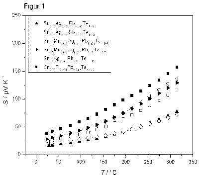
In addition, temperature-resolved measurements of the Seebeck coefficient up
to
5 300 C were carried out, which are shown in figure 1. The particular Seebeck
coefficient
is plotted against the temperature. The measurements confirm that the Sri-rich
materials do not undergo any switch from the p-conductive to the n-conductive
type
within the temperature range investigated. Individual sample slices were
analyzed. The
procedure was to balance the temperatures of the cold and hot side down to a
small
10 interval (4T < 2 K) and in this way to measure the Seebeck coefficient at
an average
temperature ((Tcod+Tnot)/2).
For comparative purposes, lead tellurides with a high lead content were
prepared, and
the temperature dependence of the Seebeck coefficient was determined. Figure 2
shows the corresponding results for different materials. The particular
Seebeck
coefficient is plotted against the temperature. The measurements confirm that
materials
with a very high lead content exhibit a switch from p-conduction to n-
conduction with
rising temperature. The systems therefore do not satisfy the requirements with
regard
to thermal stability, and the Seebeck coefficient has, depending o ; the
temperature,
very low values. In figure 2, p-L r jeans p-conduction and n-L means n-
conduction.