Note: Descriptions are shown in the official language in which they were submitted.
CA 02715481 2010-08-13
WO 2009/117717 PCT/US2009/037895
1
ADAPTIVE LINEARITY COMMUNICATION DEVICE
Claim of Priority under 35 U.S.C. 119
[0001] The present Application for Patent claims priority to Provisional
Application
No. 61/038,710 entitled "Adaptive Linear Receiver" filed March 21, 2008, and
assigned
to the assignee hereof and hereby expressly incorporated by reference herein.
BACKGROUND
Field
[0002] This invention is generally related to wireless communications, and
more
particularly, to systems and methods of constructing and operating an adaptive
linearity
communication device for a wireless communication system.
Background
[0003] Wireless communication devices may include receivers that process
incoming
signals to extract information or data from a transmitted signal. Conventional
receivers
include components that have a response dependent on bias. The bias may be a
voltage
bias and/or a current bias depending on the particular receiver component.
Typically,
the linearity of operation of the receiver component increases with the bias
that is
applied. As the bias is reduced from an optimum linearity level, the linearity
of a
receiver component decreases and the response becomes increasingly non-linear.
[0004] Intermodulation distortion (IMD) increases as the response becomes non-
linear.
IMD degrades performance of the receiver by introducing interference energy
within the
receive band. When a non-linear response is applied to two or more interfering
signals,
the signals may mix to produce IMD products (signals). Accordingly,
interfering
signals processed by the receiver component with a non-linear response may
result in
IMD signals within the receive band, although one or more of the original
interfering
signals are outside the receive band. Sensitivity and overall receiver
performance is
reduced as IMD signals increase. Unfortunately, increasing bias and operating
components in a linear mode is inefficient. Slight increases in bias and
linearity may
result in large additional power consumption. In wireless communication
devices where
power is limited, increasing bias to the receiver components may significantly
reduce
the battery life ("talk time").
[0005] Various techniques have been employed to increase the linearity of
receiver
components while minimizing the adverse affect upon the battery life. However,
the
CA 02715481 2010-08-13
WO 2009/117717 PCT/US2009/037895
2
previous attempts remain inadequate to optimize the operation of receiver
components
while conserving battery life. Therefore, there is need for improvement.
SUMMARY
[0006] Disclosed herein is a new and improved adaptive linearity communication
device and methods for use in a wireless communication system.
[0007] In accordance with an aspect, a wireless communication device having a
component having a linearity dependent upon a bias, includes a processor
configured to
change the bias in response to the detection of a connection between the
wireless
communication device and a high-capacity power source.
[0008] In accordance with another aspect, a wireless communication device
includes a
component having a linearity dependent upon a bias, and a means for changing
the bias
in response to the detection of a connection between the wireless
communication device
and a high-capacity power source.
[0009] In accordance with another aspect, a method for operating a wireless
communication device having a bias dependent component, and the device being
configured to operate in a high efficiency mode in the absence of a connection
between
the device and a high-capacity power source, comprising determining whether a
high-
capacity power source is connected to the wireless communication device, and
varying
the operation of the bias dependent component based on whether a high-capacity
power
source is connected to the wireless communication device.
[0010] In accordance with a further aspect, a computer-readable medium
embodying a
set of instructions executable by one or more processors for operating a
wireless
communication device having a bias dependent component, and the device being
configured to operate in a high efficiency mode in the absence of a connection
between
the device and a high-capacity power source, including code for determining
whether a
high-capacity power source is connected to the wireless communication device,
and
code for varying the operation of the bias dependent component based on
whether a
high-capacity power source is connected to the wireless communication device.
[0011] Other systems, methods, aspects, features, embodiments and advantages
of the
adaptive linearity communication device disclosed herein will be, or will
become,
apparent to one having ordinary skill in the art upon examination of the
following
drawings and detailed description. It is intended that all such additional
systems,
CA 02715481 2010-08-13
WO 2009/117717 PCT/US2009/037895
3
methods, aspects, features, embodiments and advantages be included within this
description, and be within the scope of the accompanying claims.
BRIEF DESCRIPTION OF THE DRAWINGS
[0012] It is to be understood that the drawings are solely for purpose of
illustration.
Furthermore, the components in the figures are not necessarily to scale,
emphasis
instead being placed upon illustrating the principles of the apparatus and
methods
disclosed herein. In the figures, like reference numerals designate
corresponding parts
throughout the different views.
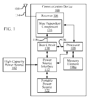
[0013] FIG. 1 is a block diagram of an exemplary wireless communication
device,
including an adaptive linearity receiver, and a high-capacity power source.
[0014] FIG. 2 is a graphical illustration of an exemplar frequency spectrum
that may be
received by the wireless communication device of FIG. 1.
[0015] FIG. 3 is a more detailed block diagram of the wireless communication
device of
FIG. 1 illustrating that the wireless communication device may include a
receiver front
end having a component with a linearity that is dependent on bias.
[0016] FIG. 4 is a flow chart of a method of adjusting the linearity of a
wireless
communication device, such as, but not limited to, the wireless communication
device
of FIG. 1 and FIG. 3.
[0017] FIG. 5 is a second flow chart of a method of adjusting the linearity of
a wireless
communication device, such as, but not limited to, the wireless communication
device
of FIG. 1 and FIG. 3.
[0018] FIG. 6 is a third flow chart of a method of adjusting the linearity of
a wireless
communication device, such as, but not limited to, the wireless communication
device
of FIG. 1 and FIG. 3.
DETAILED DESCRIPTION
[0019] The following detailed description, which references to and
incorporates the
drawings, describes and illustrates one or more specific embodiments. These
embodiments, offered not to limit but only to exemplify and teach, are shown
and
described in sufficient detail to enable those skilled in the art to practice
what is
claimed. Thus, for the sake of brevity, the description may omit certain
information
known to those of skill in the art.
[0020] The word "exemplary" is used herein to mean "serving as an example,
instance, or illustration." Any embodiment or variant described herein as
"exemplary"
CA 02715481 2010-08-13
WO 2009/117717 PCT/US2009/037895
4
is not necessarily to be construed as preferred or advantageous over other
embodiments
or variants. All of the embodiments and variants described in this description
are
exemplary embodiments and variants provided to enable persons skilled in the
art to
make and use the invention, and not necessarily to limit the scope of legal
protection
afforded the appended claims.
[0021] FIG. 1 is a block diagram of an exemplary wireless communication device
100
and a high-capacity power source 102. Communication device 100 may include an
antenna 104, a receiver 106, a processor 108, a memory element 108a, a bias
circuit
110, a power source interface 112, and a portable power source 122. The
antenna 104
may receive incoming signals on the line 114. The incoming signal may include,
for
example, a carrier signal and various interfering signals, and may be based on
various
protocols including, but not limited to, ultra-wide band (UWB). The incoming
signal
may be provided to the receiver 106 for processing. The operation of the
receiver 106
may generally be determined by the relationships and interconnections between
receiver
components, and upon the various control signals received by the receiver 106
from
other components of the communication device 100, such as the processor 108,
and/or
upon the incoming signal on the line 114.
[0022] Among other internal components, the receiver 106 may include bias
dependent
components 116. The bias dependent components 116 may be numerous components
whose linearity of operation may depend upon the bias provided to the bias
dependent
components 116, for example, but not limited to, mixers, filters, amplifiers,
low noise
amplifiers, analog to digital converters (ADCs), and/or combinations of such
devices.
In FIG. 1, the bias for the bias dependent components 116 may be provided on
line 118.
[0023] The communication device 100 may be mobile or stationary, and may
communicate with one or more base stations (not shown). Examples of the
wireless
communication device 100 include, but are not limited to, cellular telephones,
personal
digital assistances (PDAs), laptop computers, PC cards, compact flash devices,
external
modems and internal modems. In many communication systems, the communication
device 100 transmits and receives data packets through one or more modem pool
transceivers to an HDR base station controller (not shown). An access network
(not
shown) may transport data packets between multiple communication devices, such
as
the communication device 100. The access network may be further connected to
additional networks (not shown) outside the access network, such as a
corporate intranet
CA 02715481 2010-08-13
WO 2009/117717 PCT/US2009/037895
or the Internet, and may transport data packets between each access terminal
and such
outside networks. Though shown for illustrative purposes having the antenna
104, the
communication device 100, may be any data device that communicates through a
wireless channel or through a wired channel, for example using fiber optic or
coaxial
cables.
[0024] The bias may be a current bias, a voltage bias, or a combination of the
two, for
different components within the receiver 106. As described in further detail
below, the
bias may be increased when certain conditions are met in order to increase the
linearity
of the bias dependent components 116 and to decrease intermodulation
distortion
(IMD).
[0025] The bias may be provided, controlled and managed through the bias
circuit 110
responsive to a control signals generated by the processor 108 and provided to
the bias
circuit 110 on a line 120. The processor 108, using any required peripherals
and/or
input/output devices, may manage the bias provided by the bias circuit 110 and
may
detect the connection of the high-capacity power source 102 through the power
source
interface 112. Based upon various conditions described and illustrated herein,
the
processor 108 may communicate with the bias circuit 110 in order to operate
the bias
dependent components 116 in various manners, including a high efficiency mode
and a
high linearity mode. The control signal on the line 120 may include, but is
not limited
to, providing two or more bias points for setting the bias of the one or more
bias
dependent components 116.
[0026] Any of numerous criteria may be used to determine whether the bias
should be
increased or decreased to place one or more of the bias dependent components
116 in a
high efficiency mode or a high linearity mode. In one example, the bias is
increased,
and one or more of the bias dependent components 116 are operated in high
linearity
mode, when the high-capacity power source 102 is connected. In another
example, the
bias is only increased if the high-capacity power source 102 is connected and
interference on the line 114 is detected. Interference may be in a number of
forms,
including, but not limited to IMD signals and cross-modulation. For another
example,
the bias is increased if the high-capacity power source 102 is connected and
the wireless
communication system is operating in a jurisdiction that requires a high
linearity mode
of operation. Such jurisdictions may call for high linearity operation to
avoid
interference among wireless communication systems in close proximity.
CA 02715481 2010-08-13
WO 2009/117717 PCT/US2009/037895
6
[0027] The interference may be detected within a particular frequency band or
as an
overall energy level outside the reception band. Further, the interference may
be
detected by observing IMD. Where the criteria for increasing the bias includes
detecting interference, the receiver 106 may include circuitry and/or software
for
evaluating the signals received through the antenna 104. Those having ordinary
skill in
the art are familiar with such circuitry and/or software for evaluating the
signals
received.
[0028] The power source interface 112 may include a connector for connecting
to the
high-capacity power source 102. In some circumstances, the power source
interface
112 may also include circuitry, such as power conversion, power regulation and
switching circuitry.
[0029] The high-capacity power source 102 connects to the power source
interface 112.
The high-capacity power source 102 may be any type of power source that is
capable of
providing power to communication device 100 at a level that does not diminish
operational parameters, for example, but not limited to, power provided or
derived from
alternating current (AC) outlets, wireless power (such as RF to DC power
conversion
via near-field inductive coils) devices, inductive mats and vehicle electrical
systems.
The high-capacity power source 102 may be an AC/DC adapter plugged into a 110
volt
AC outlet, or alternatively, the high-capacity power source 102 may be a
direct
connection to the AC 110 volt outlet. Further, the high-capacity power source
102 may
be a 12 volt supply from a vehicle.
[0030] The processor 108 may be any combination of hardware, software and/or
firmware that executes the functions described herein as well as performing
overall
management functions of the device. The processor 108 may also perform other
functions associated with the operation of the wireless communication device
100 as is
known to those having skill in the art. The memory element 108a may be
connected to
the processor 108 for storing software code and other data.
[0031] The portable power source 122 may provide temporary power to the
communication device 100, for example, when the high-capacity power source 102
is
not connected to the communication device 100. In some situations, the
portable power
source 122 may be charged by the high-capacity power source 102, and/or may
provide
power to the communication device 100 when the high-capacity power source 102
is
disconnected. The portable power source 122 may be internal to the
communication
CA 02715481 2010-08-13
WO 2009/117717 PCT/US2009/037895
7
device 100 or may be an external component that is connected to the
communication
device 100. The portable power source 122 may be any power source or source
that can
be transported with the communication device 100, for example, but not limited
to, a
battery, solar cells, capacitors, and inductive mats. The power source
interface 112 may
include circuitry for managing the charging of the portable power source 122.
[0032] The high-capacity power source 102 may be distinguished from the
portable
power source 122 in that increasing the power consumption of the device 100
when
connected to the high-capacity power source 102 does not limit any performance
parameters of the communication device 100, whereas increasing the power
consumption of the communication device 100 when connected only to the
portable
power source 122 may result in performance consequences. Examples of such
performance consequences include a decrease in operational time ("talk time"),
a
decrease in transmission power, a decrease in illumination intensity, a
decrease in
display intensity, and a decrease in audio power level.
[0033] The bias circuit 110 and/or processor 108 may set, based on, for
example, the
connection status of the high-capacity power source 102, the bias to at least
the bias
dependent component 116. In the exemplary embodiment, the processor 108
generates
a control signal on line 120 that sets the bias circuit 110 to provide a bias
to one or more
bias dependent components 116. The control signal on line 120 may directly
relate to a
bias level, and/or may provide a reference point to which the bias level is
set. For
example, where the bias circuit 110 includes a feedback loop that maintains
the bias
based on current consumption (or some other parameter), the control signal on
line 120
may provide a reference level for the loop.
[0034] FIG. 2 is a graphical illustration of an exemplar frequency spectrum
200 that
may be received by the wireless communication device 100 of FIG. 1. The
frequency
spectrum 200 shows interference signals 202 and 204 and an intermodulation
distortion
(IMD) signal 206 within a receive band 208. The IMD signal 206 may be caused
by at
least the two interference signals 202 and 204.
[0035] Non-linearity in a receiver can cause signals outside of receive band,
such as the
receive band 208, to mix and form an IMD signal, such as the IMD signal 206,
within
the receive band. The IMD signal 206 may be a sum and/or difference of various
harmonics of various interfering signals. For example, if one interfering
signal has a
frequency of F1, such as signal 202, and another has a frequency of F2, such
as signal
CA 02715481 2010-08-13
WO 2009/117717 PCT/US2009/037895
8
204, potential first order IMD signal frequencies include FIMD = Fi + F2 and
FIMD = Fi -
F2. Potential second order IMD signal frequencies include FIMD= 2F1 + F2,
FIMD= 2F1
- F2, FIMD= Fi + 2Fz and FIMD= Fi - 2F2. Other IMD orders may be present
depending
on the particular circumstances. The amplitude and energy level of an IMD
signal, such
as the IMD signal 206, may depend on the linearity of the receiver, such as
the receiver
106, which may depend upon the linearity of receiver components, such as the
bias
dependent components 116.
[0036] For the case illustrated in FIG. 2, for a first bias, IMD signal 206
may have a
first amplitude 210. When the bias is increased to a second bias, IMD signal
206 may
have a lower amplitude 212. Accordingly, FIG. 2 provides a graphical example
of IMD
signal 206 during the high efficiency mode, where IMD signal 206 may have
amplitude
210, and the high linearity mode, where a greater bias may be provided to one
or more
of the bias dependent components 116, and where the IMD signal 206 may have
the
lower amplitude 212.
[0037] FIG. 3 is a more detailed block diagram of the wireless communication
device
100 of FIG. 1 illustrating that the receiver 106 may include a receiver front
end 302 and
a receiver back end 304. The receiver front end 302 generally includes bias
dependent
components 116 as illustrated in FIG. 1. However, it is within the scope of
the
invention that the bias dependent components 116 may be included in any
portion of the
communication device 100. The receiver front end 302 typically includes analog
components such as mixers, filters, low noise amplifiers and analog to digital
converters
(ADCs). The bias dependent components 116 may include such analog components.
[0038] The receiver front end 302 may receive the incoming signal on line 114
and may
convert the carrier signal to a baseband and/or an intermediate frequency
signal, and
then provide the baseband and/or intermediate signal to the receiver back end
304 on a
line 306. The receiver back end 304 may further process the baseband and/or an
intermediate frequency signal to recover a received data 308.
[0039] The receiver back end 304 typically includes digital signal processing
components that are power efficient, where bias and power consumption are less
of an
issue than in the receiver front end 302. In some cases, at least some of the
receiver
back end functions may be implemented within a controller or a processor,
microprocessor, application specific integrated circuit (ASIC), or other
processor
arrangement. In addition, some or all of the functions of the processor 108
may be
CA 02715481 2010-08-13
WO 2009/117717 PCT/US2009/037895
9
implemented on or in the same chip or processor used to perform functions
associated
with the receiver back end 304.
[0040] Processor 108 may establish two bias points with the control signal on
line 120.
Processor 108 may cause communication device 100 to operate in a high
efficiency
mode wherein the receiver 106 experiences relatively low power consumption and
a
relatively low linear response of one or more bias dependent components 116 by
controlling the bias signal on line 118 to meet, for example, a threshold or
minimum
performance requirement. Processor 108 may also cause communication device 100
to
operate in a high linearity mode wherein the receiver 106 experiences
relatively high
power consumption and a relatively high linear response of one or more bias
dependents
components 116 by controlling the bias signal on line 118.
[0041] As an example, processor 108 may set the bias to the high linearity
mode when
processor 108 detects the connection of the high-capacity power source 102 to
power
source interface 112. Otherwise, the bias may be set to the high efficiency
mode with
lower linearity. As a second example, processor 108 may set the bias to the
high
linearity mode only when processor 108 detects the high-capacity power source
102 is
connected to power source interface 112 and an interfering signal is detected
on line
114. As non-limiting examples, the interfering signal may be detected using a
spectral
analysis and/or may be detected by determining that an IMD signal, for example
IMD
signal 206, is above a threshold.
[0042] FIG. 4 is a flow chart of an exemplary method 400 of adjusting the
linearity of a
wireless communication device, such as, but not limited to, the wireless
communication
device 100 of FIG. 1 and FIG. 3. Exemplary method 400, though not limited by
any
particular hardware, may be performed, at least partly, by executing code
using
processor 108. In addition, method 400 may be performed by any combination of
hardware, software, and/or firmware.
[0043] In block 402 of method 400, a wireless communication device, for
example
wireless communication device 100, may be directed to operate in a high
efficiency
mode. One manner of operating in a high efficiency mode includes providing an
instruction to a bias circuit, for example bias circuit 110, to provide a bias
signal to
operate at least one component, for example one or more bias dependent
components
116, in a high efficiency mode.
CA 02715481 2010-08-13
WO 2009/117717 PCT/US2009/037895
[0044] In block 404 of method 400, it is determined whether a high-capacity
power
source, for example the high-capacity power source 102, has been connected to
the
wireless communication device. In an exemplary embodiment, detection circuitry
may
determine if power is provided to the power source interface 112 from the high-
capacity
power source 102, such as an AC adapter or a 12 volt vehicle adapter. The
determination of whether the high-capacity power source has been connected may
be
made according to a variety of criteria, such as but not limited to, based
upon a
preprogrammed interval and/or based on a user selectable setting. If the high-
capacity
power source is connected, method 400 continues to block 406. Otherwise,
method 400
recycles to block 402.
[0045] In block 406, a bias circuit, for example bias circuit 110, is directed
to provide a
bias signal to operate at least one component, for example one or more bias
dependent
components 116, in a high linearity mode. The high linearity mode may result
in the
receiver, for example, the receiver 106, operating with a more linear response
than when
the receiver may operate in the high efficiency mode. In most situations, the
power
consumed by the receiver will be greater when operating in the high linearity
mode. In
other embodiments, the high linearity mode may include variable linearity
settings that
may depend upon various factors, such as, but not limited to, the level of any
interference affecting the receipt of the received data 308, and the level of
charge of the
portable power source 122. After block 406, method 400 may return to block
404.
[0046] In the event a high-capacity power source is disconnected, the method
may then
return to block 402 from block 404. The high efficiency mode of block 402 may
result
in the receiver, for example, the receiver 106, operating with a less linear
response than
when the receiver may operate in the high linearity mode.
[0047] FIG. 5 is a flow chart of a second exemplary method 500 of adjusting
the
linearity of a wireless communication device, such as, but not limited to, the
wireless
communication device 100 of FIG. 1 and FIG. 3. As with method 400, exemplary
method 500, though not limited by any particular hardware, may be performed,
at least
partly, by executing code using processor 108. In addition, method 500 may be
performed by any combination of hardware, software, and/or firmware.
[0048] As illustrated in FIG. 5, method 500 includes several blocks that have
been
previously described in regard to method 400. However, in method 500, if a
high-
capacity power source is connected in block 404, method 500 continues to block
502
CA 02715481 2010-08-13
WO 2009/117717 PCT/US2009/037895
11
rather than directly to block 406. Otherwise, method 500 recycles from block
404 to
block 402 as with method 400.
[0049] In block 502, it is determined whether interference has been detected,
for
example, interference may be detected on line 114 of the wireless
communication
device 100. In the exemplary embodiment, received signals are analyzed to
determine if
there are at least two interfering signals, for example interference signals
202 and 204,
that may cause IMD, such as IMD signal 206, with a receive band. Other
techniques
for determining whether interference is present include evaluating the
amplitude of the
IMD signal, and determining interference is present if the amplitude is above
a
threshold. If the interference is detected, method 500 continues to block 406.
Otherwise, method 500 returns to block 402.
[0050] FIG. 6 is a flow chart of a further exemplary method 600 of adjusting
the
linearity of a wireless communication device, such as, but not limited to, the
wireless
communication device 100 of FIG. 1 and FIG. 3. As with methods 400 and 500,
exemplary method 600, though not limited by any particular hardware, may be
performed, at least partly, by executing code using processor 108. In
addition, method
500 may be performed by any combination of hardware, software, and/or
firmware.
[0051] As illustrated in FIG. 6, method 600 includes several blocks that have
been
previously described in regard to methods 400 and 500. However, method 600
includes
additional block 602 and 604.
[0052] In block 602, it is determined whether the high linearity mode of
operation has
been disabled. The high linearity mode may be disabled for a variety of reason
and in a
number of manners, such as but not limited to, through a user option, through
a factory
setting, through an equipment manufacturer setting, and/or based on geography
or
jurisdictional requirements or lack thereof. In the event the high linearity
mode is
disabled, the method 600 may return to block 402 and the wireless
communication
device may continue to operate in a high efficiency mode. In the event the
high
linearity mode is not disabled, method 600 may continue to block 404.
[0053] Method 600 may operate in the manner previously described in regard to
blocks
404 and 502. In the event interference is detected in block 502, method 600
may
continue to block 604. In block 604, it is determined whether the level of the
charge of
a portable power source, for example portable power source 122, exceeds a
threshold
indicating sufficient charge to allow the wireless communication device 100 to
operate
CA 02715481 2010-08-13
WO 2009/117717 PCT/US2009/037895
12
in a high linearity mode, without overly compromising the ability of the high-
capacity
power source, for example the high-capacity power source 102, to charge the
portable
power source, or to perform other power intensive activities. In some
situations, the
threshold may be set low since the high-capacity power source 102 may be
capable of
charging the portable power source 122 while also providing sufficient power
to operate
the receiver 106 without adverse consequences. If the charge of the portable
power
source does not exceed the threshold, method 600 may recycle to block 402. If
the
charge of the portable power source does exceed the threshold, method 600
continues to
block 406.
[0054] The functionality, operations and architecture depicted by the blocks
of methods
400, 500 and 600 may be implemented using modules, segments, and/or portions
of
software and/or firmware code. The modules, segments, and/or portions of code
include
one or more executable instructions for implementing the specified logical
function(s).
In some implementations, the functions noted in the blocks may occur in a
different
order than that shown in FIG. 4, FIG. 5 and FIG. 6. For example, two blocks
shown in
succession in FIG. 4, FIG. 5 and/or FIG 6 may be executed concurrently, or the
blocks
may sometimes be executed in another order, depending upon the functionality
involved.
[0055] Those of skill in the art would understand that information and signals
may be
represented using any of a variety of different technologies and techniques.
For
example, data, instructions, commands, information, signals, bits, symbols,
and chips
that may be referenced throughout the above description may be represented by
voltages, currents, electromagnetic waves, magnetic fields or particles,
optical fields or
particles, or any combination thereof.
[0056] Those of skill would further appreciate that the various illustrative
logical
blocks, modules, circuits, and algorithm steps described in connection with
the
embodiments disclosed herein may be implemented as electronic hardware,
computer
software, or combinations of both. To clearly illustrate this
interchangeability of
hardware and software, various illustrative components, blocks, modules,
circuits, and
steps have been described above generally in terms of their functionality.
Whether such
functionality is implemented as hardware or software depends upon the
particular
application and design constraints imposed on the overall system. Skilled
artisans may
implement the described functionality in varying ways for each particular
application,
CA 02715481 2010-08-13
WO 2009/117717 PCT/US2009/037895
13
but such implementation decisions should not be interpreted as causing a
departure from
the scope of the present invention.
[0057] The various illustrative logical blocks, modules, and circuits
described in
connection with the embodiments disclosed herein may be implemented or
performed
with a general purpose processor, a digital signal processor (DSP), an
application
specific integrated circuit (ASIC), a field programmable gate array (FPGA) or
other
programmable logic device, discrete gate or transistor logic, discrete
hardware
components, or any combination thereof designed to perform the functions
described
herein. A general purpose processor may be a microprocessor, but in the
alternative, the
processor may be any conventional processor, controller, microcontroller, or
state
machine. A processor may also be implemented as a combination of computing
devices, e.g., a combination of a DSP and a microprocessor, a plurality of
microprocessors, one or more microprocessors in conjunction with a DSP core,
or any
other such configuration.
[0058] The steps of a method or algorithm described in connection with the
embodiments disclosed herein may be embodied directly in hardware, in a
software
module executed by a processor, or in a combination of the two. A software
module
may reside in RAM memory, flash memory, ROM memory, EPROM memory,
EEPROM memory, registers, hard disk, a removable disk, a CD-ROM, or any other
form of storage medium known in the art. An exemplary storage medium is
coupled to
the processor such the processor can read information from, and write
information to,
the storage medium. In the alternative, the storage medium may be integral to
the
processor. The processor and the storage medium may reside in an ASIC. The
ASIC
may reside in a user terminal. In the alternative, the processor and the
storage medium
may reside as discrete components in a user terminal.
[0059] As mentioned above, the functions described may be implemented in
hardware,
software, firmware, or any combination thereof. If implemented in software,
the
functions may be stored on or transmitted over as one or more instructions or
code on a
computer-readable medium. Computer-readable media includes both computer
storage
media and communication media including any medium that facilitates transfer
of a
computer program from one place to another. A storage media may be any
available
media that can be accessed by a computer. By way of example, and not
limitation, such
computer-readable media can comprise RAM, ROM, EEPROM, CD-ROM or other
CA 02715481 2010-08-13
WO 2009/117717 PCT/US2009/037895
14
optical disk storage, magnetic disk storage or other magnetic storage devices,
or any
other medium that can be used to carry or store desired program code in the
form of
instructions or data structures and that can be accessed by a computer. Also,
any
connection is properly termed a computer-readable medium. For example, if the
software is transmitted from a website, server, or other remote source using a
coaxial
cable, fiber optic cable, twisted pair, digital subscriber line (DSL), or
wireless
technologies such as infrared, radio, and microwave, then the coaxial cable,
fiber optic
cable, twisted pair, DSL, or wireless technologies such as infrared, radio,
and
microwave are included in the definition of medium. Disk and disc, as used
herein,
includes compact disc (CD), laser disc, optical disc, digital versatile disc
(DVD), floppy
disk and blu-ray disc where disks usually reproduce data magnetically, while
discs
reproduce data optically with lasers. Combinations of the above should also be
included
within the scope of computer-readable media.
[00601 The above description of the disclosed embodiments is provided to
enable any
person skilled in the art to make or use that which is defined by the appended
claims.
The following claims are not intended to be limited to the disclosed
embodiments.
Other embodiments and modifications will readily occur to those of ordinary
skill in the
art in view of these teachings. Therefore, the following claims are intended
to cover all
such embodiments and modifications when viewed in conjunction with the above
specification and accompanying drawings.
[00611 WHAT IS CLAIMED IS: