Note: Descriptions are shown in the official language in which they were submitted.
CA 02715884 2013-04-17
54106-559
1
ADJUSTABLE ELECTRICAL PROBES FOR CIRCUIT BREAKER TESTER
BACKGROUND
1. Technical Field
This disclosure relates to electrical test fixtures,
and more particularly, to a device and method for
adjustable configuring test probes to perform testing on
different electrical component configurations.
2. Description of the Related Art
In circuit breakers, a location of a lug and neutral
strap may vary between different designs. In production,
the different designs may need to employ the same test
equipment, but the differences in the designs preclude
such use. In conventional systems, functional
production fixtures use electrical probes that are fixed
in a housing and are not adjustable. To accommodate
different components to be tested, the probes are
manually bent by technicians to attempt to properly
CA 02715884 2010-08-17
WO 2009/105181
PCT/US2009/000969
2
interface this connection with the component to be
tested. Typically, the probes are bent by the use of a
hammer or pliers. Due to these bending methods of the
probes, the accuracy can vary greatly between testers and
components to be tested. For example, a breaker may be
non-conforming in one tester while passing in a different
tester. This may be due to the location of the bent
probes and the quality of the connection.
Further, the probes and the test fixtures are subject
to damage due to the bending methods. Tooling of the
probe is an additional disadvantage to the existing
design since the probes usually are fabricated to
prevent rotation of the probes during operation. For
example, the electrical probes are hexagonal in shape
and require special tooling to produce them. This type
of design is employed so that the electrical probes do
not rotate.
Electrical probes are usually supported in a single
block configuration that cannot be adjusted in any
manner. This requires that the location of the probes
be exactly in position so that they interface with the
line lug and neutral strap of a circuit breaker, for
example. In some cases, the lugs may touch the plastic
housing of the circuit breaker missing their target
rather than making an electrical contact with the lug.
CA 02715884 2010-08-17
WO 2009/105181
PCT/US2009/000969
3
The probe alignment becomes an issue in manufacturing
during functional testing since circuit breaker
designs may be different. Without proper electrical
contact, the breakers could fail testing due to a lack
of electrical continuity. Any design changes in the lug
area of the breaker could require adjustments in the
functional tester itself. Typically,
manufacturing will manually adjust the probes to meet
the new design. However, this manual bending is not
controlled to any specification, and the amount of
bending varies from tester to tester and operator to
operator.
SUMMARY OF THE INVENTION
An electrical probe assembly includes a first probe
housing pivotally connected to a base structure and
receiving a first probe therein. The first probe is
configured to interface with a first contact of an
electrical component. A second probe housing is
pivotally connected to the base structure and receives a
second probe therein. The second probe is configured to
interface with a second contact of the electrical
component wherein the first and second contacts have a
spatial relationship therebetween. An adjustment
mechanism is connected to the first and second housing
CA 02715884 2010-08-17
WO 2009/105181
PCT/US2009/000969
4
and configured to independently adjust an amount of
rotation of the each of the housings to accommodate the
spatial relationship.
An electrical probe assembly for interfacing with a
plurality of different circuit breaker designs includes
a plurality of probe housings each having a corresponding
test probe protruding therefrom. A pivot pin is
configured to pass through the plurality of housings to
pivotally connect the housings to a base structure such
that the plurality of housings independently rotate about
a same axis. An adjustment mechanism is connected to the
plurality of housings and configured to independently
adjust an amount of rotation of the each of the housings
to accommodate different spatial relationships for
contacts of different circuit breaker designs.
A method for testing a circuit breaker includes
providing an electrical probe assembly having a first
probe housing pivotally connected to a base structure and
receiving a first probe therein, the first probe being
configured to interface with a first contact of a circuit
breaker, a second probe housing pivotally connected to
the base structure and receiving a second probe therein,
the second probe being configured to interface with a
second contact of the circuit breaker wherein the first
and second contacts have a spatial relationship
CA 02715884 2013-04-17
54106-559
therebetween, and an adjustment mechanism connected to the first
and second housing; adjusting the adjustment mechanism to
independently adjust an amount of rotation of each of the
housings to accommodate the spatial relationship of contacts for
5 a circuit breaker design; and testing the circuit breaker.
According to one aspect of the present invention, there
is provided an electrical probe assembly, comprising: a first
probe housing pivotally connected to a base structure and
receiving a first probe therein, the first probe being configured
to interface with a first contact of an electrical component; a
second probe housing pivotally connected to the base structure
and receiving a second probe therein, the second probe being
configured to interface with a second contact of the electrical
component wherein the first and second contacts have a spatial
relationship therebetween, and wherein a pivoting mechanism
permits independent pivotal motion of the first probe housing and
the second probe housing relative to the base structure; and an
adjustment mechanism connected to each of the first and second
housing and the base structure and configured to independently
adjust an amount of rotation of the each of the housings relative
to the base structure to accommodate the spatial relationship.
According to another aspect of the present invention,
there is provided an electrical probe assembly, comprising: a
first probe housing pivotally connected to a base structure and
receiving a first probe therein, the first probe being configured
to interface with a first contact of an electrical component; a
second probe housing pivotally connected to the base structure
and receiving a second probe therein, the second probe being
configured to interface with a second contact of the electrical
CA 02715884 2013-04-17
54106-559
5a
component wherein the first and second contacts have a spatial
relationship therebetween; an adjustment mechanism connected to
the first and second housing and configured to independently
adjust an amount of rotation of the each of the housings to
accommodate the spatial relationship wherein the adjustment
mechanism includes an adjustment screw; and a biasing device
disposed on an opposing side from the adjustment screw of at
least one of the first and second housings for providing a
restoring force to permit bidirectional adjustment.
According to still another aspect of the present
invention, there is provided an electrical probe assembly,
comprising: a first probe housing pivotally connected to a base
structure and receiving a first probe therein, the first probe
being configured to interface with a first contact of an
electrical component; a second probe housing pivotally connected
to the base structure and receiving a second probe therein, the
second probe being configured to interface with a second contact
of the electrical component wherein the first and second contacts
have a spatial relationship therebetween; a third probe housing
pivotally connected to the base structure and receiving a third
probe therein, the third probe being configured to interface with
a third contact of the electrical component; and an adjustment
mechanism connected to the first and second housing and
configured to independently adjust an amount of rotation of the
each of the housings to accommodate the spatial relationship.
According to yet another aspect of the present
invention, there is provided an electrical probe assembly for
interfacing with a plurality of different circuit breaker
designs, comprising: a plurality of probe housings each having a
corresponding test probe extending therefrom; a pivot pin
CA 02715884 2013-04-17
54106-559
5b
configured to pass through the plurality of housings to pivotally
connect the housings to a base structure such that the plurality
of housings independently rotate about a same axis; and an
adjustment mechanism connected to each of the plurality of
housings and the base structure and configured to independently
adjust an amount of rotation of the each of the housings to
accommodate different spatial relationships for contacts of
different circuit breaker designs wherein the pivot pin permits
independent pivotal motion of each of the housings relative to
the base structure.
According to a further aspect of the present invention,
there is provided a method for testing a circuit breaker,
comprising: providing an electrical probe assembly having a first
probe housing pivotally connected to a base structure and
receiving a first probe therein, the first probe being configured
to interface with a first contact of a circuit breaker, a second
probe housing pivotally connected to the base structure and
receiving a second probe therein, the second probe being
configured to interface with a second contact of the circuit
breaker wherein the first and second contacts have a spatial
relationship therebetween, and an adjustment mechanism connected
to each of the first and second housing and the base structure,
and wherein a pivoting mechanism permits independent pivotal
motion of the first probe housing and the second probe housing
relative to the base structure; adjusting the adjustment
mechanism to independently adjust an amount of rotation of each
of the housings to accommodate the spatial relationship of
contacts for a circuit breaker design; and testing the circuit
breaker by contacting the first and second probes with the first
and second contacts.
CA 02715884 2013-04-17
54106-559
These and other objects, features and advantages of
the present invention will become apparent from the
following detailed description of illustrative
embodiments thereof, which is to be read in connection
with the accompanying drawings.
BRIEF DESCRIPTION OF DRAWINGS
This disclosure will present in detail the following
description of preferred embodiments with reference to
the following figures wherein:
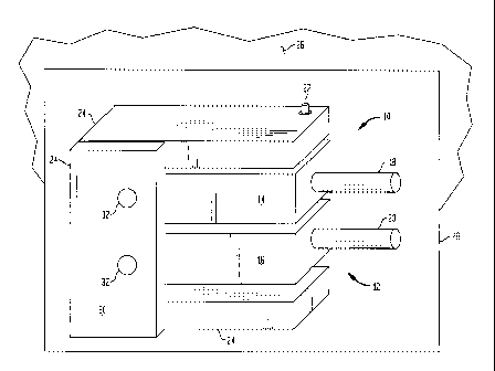
FIG. 1 is a perspective view of a probe assembly
employed in testing electrical components in accordance
with one illustrative embodiment;
FIG. 2 is a partial cross-sectional view of the
assembly of FIG. 1 showing an illustrative adjustment
mechanism in accordance with one illustrative embodiment;
FIG. 3 is a partial cross-sectional view of the
assembly of FIG. 1 showing a pivot pin arrangement in
accordance with one illustrative embodiment;
CA 02715884 2010-08-17
WO 2009/105181
PCT/US2009/000969
. 6
FIG. 4 is a front view showing an anti-rotation key
for preventing rotation of test probes in accordance with
one illustrative embodiment;
FIG. 5 is a perspective view of a probe assembly
employed in testing electrical components showing a three
probe arrangement for testing a circuit breaker in
accordance with one illustrative embodiment.
DETAILED DESCRIPTION OF PREFERRED EMBODIMENTS
The present invention provides adjustable electrical
probes for functional testers that interface with a
circuit breaker. The present principles may be used to
retrofit existing functional testers in manufacturing
facilities or may be part of the design of new functional
testers. In one illustrative example, the probes may be
employed in conjunction with any of a plurality of
commercially available functional testers, e.g., for
manufacture testing circuit breakers. The tester provides
an electrical connection interface between a circuit
breaker to be tested and the tester itself. This
interface may benefit from the present principles,
which would then be employed to test the circuit
breaker in manufacturing to ensure the end product
meets test standards.
CA 02715884 2010-08-17
WO 2009/105181
PCT/US2009/000969
7
An improved electrical probe is provided to interface
with the breaker. This probe provides the ability to
make adjustments to a probe location to ensure
electrical connection can be made even if a breaker
design has changed. For example, a lug position or
neutral strap position may have been related in a breaker
design. In one embodiment, the probe employs industry
standard bar stock as a core material to ensure easy
replacement of the probe connections. To address the
anti-rotation needed for the electrical probes, a key
located in the probe housing may be employed, among other
things.
The present embodiments will be described in terms of
a probe assembly for a circuit breaker tester; however,
the present principles are not limited to the
illustrative example and may be employed with other
electrical component testers or even other devices where
adjustments are needed to properly interface two
components. All statements herein reciting principles,
aspects, and embodiments of the invention, as well as
specific examples thereof, are intended to encompass both
structural and functional equivalents thereof.
Additionally, it is intended that such equivalents
include both currently known equivalents as well as
equivalents developed in the future (i.e., any elements
CA 02715884 2010-08-17
WO 2009/105181
PCT/US2009/000969
8
developed that perform the same function, regardless of
structure). Thus, for example, it will be appreciated by
those skilled in the art that the block diagrams
presented herein represent conceptual views of
illustrative system components and/or circuitry embodying
the principles of the invention.
Referring now in specific detail to the drawings in
which like reference numerals identify similar or
identical elements throughout the several views, and
initially to FIG. 1, an adjustable probe assembly 10 is
shown in accordance with one illustrative embodiment.
Assembly 10 provides a probe interface 12 configured to
generally interface with a single pole circuit breaker
(not shown) in accordance with one embodiment. The
interface 12 includes probe housings 14 and 16. Each
probe housing 14 and 16 respectively includes an
electrical probe 18 and 20. As illustratively
depicted, the probe 18 corresponds to a lug probe and
the probe 20 corresponds to a neutral probe.
Each electrical probe 18 and 20 is mounted within
its respective probe housing 14 and 16, which are
independently positionable relative to each other. A
pivot pin 22 or other pivoting mechanism permits pivotal
motion of each of housings 14 and 16 relative to a base
structure such as support blocks 24 or other structures.
CA 02715884 2010-08-17
WO 2009/105181
PCT/US2009/000969
9
Support block(s) 24 is mountable on or connectable to a
tester 26. In the example, the tester 26 includes a
plate 28 mounted thereon. The interface between the
tester 26 and the plate 28 may include bolts or other
hardware (not shown) to secure the support block to the
plate 28, which in turn, is supported by the tester 26.
The plate 28 provides electrical lines to be routed from
the tester 26 to the probe housings 14 and 16 to permit
electrical testing using the probes 18 and 20.
Support block 24 includes a portion 30 that partially
encloses the probe housings 14 and 16. Portion 30
provides a support area configured with manual or
automatic adjustment controls for rotating the probes
housing 14 and 16 thereby changing the angle of probes 18
and 20 to provide a desired adjustment. An adjustment
mechanism 32 is illustratively depicted as an adjustment
screw for each housing 14 and 16; however, the adjustment
mechanism 32 may include any number of mechanisms such
as, e.g., a servo, a thumb or power screw, a cammed
adjustment member, a pneumatic cylinder, a hydraulic
cylinder or any other suitable device.
Referring to FIG. 2, a cut away view of the portion
30 of support block 24 and plate 28 shows the housing 16
of the neutral probe 20 for illustration purposes. The
housing 14 for the lug probe 18 includes a similar
CA 02715884 2010-08-17
WO 2009/105181
PCT/US2009/000969
structure. The portion 30 of the support block 24
supports the adjustment mechanism 32, in this case, an
adjustment screw 34. The adjustment screw 34 may be
advanced or withdrawn from the position 30 in accordance
with its threads. A jam nut 36 may be employed to secure
the position of the screw 34 once the appropriate
position is achieved. In this case, a biasing member 35
is employed at a position opposite the adjustment screw
34 to provide a restoring force to the housing 16. The
biasing member 35 may include a compression spring,
Belleville washers, a pneumatic chamber, etc. It should
be noted that depending on the adjustment mechanism
selected the biasing member 35 is optional. For example,
if the adjustment screw 34 is attached with a bearing-
like connection to the housing 16, the screw 32 may be
employed as both an advancing and withdrawing adjustment
member.
The housing 16 (and housing 14) has a pivot hole 38
formed therethrough to receive a pivot pin 22. In this
way, a pivot action in the direction of arrow "A" is
provided to adjust the housings 14 and 16 and thereby
adjust the positions of probes 18 and 20.
Advantageously, both probe housings 14 and 16 can
rotate freely about a single axis (pivot pin 22). The
pivot pin 22 is supported in a lower portion of the
CA 02715884 2010-08-17
WO 2009/105181
PCT/US2009/000969
11
support block 24 and held in a top portion of the
support block 24 by a retaining clip 44 (see FIG. 3).
Both probe housings 14 and 16 may have a recessed area
39 on the back side to capture one end of a compression
spring 35. An opposite end of the spring 35 would
rest on the existing mounting plate 28 (or support block
24 depending on the design) and provide a force that
would bias the probe housings 14 and 16. If the spring
35 needs to be captured, then a locating pin 37 may be
provided for the spring 35.
Referring to FIG. 3, an illustrative arrangement of
the pivot pin 22 is shown. Support block 24 includes a
pivot hole 40 therein which receives the pivot pin 22
therein. The pivot pin 22 passes through both housings
14 and 16 and is seated in a recess 42 on a lower portion
of the support block 24. A retaining clip or cotter pin
44 may be employed to prevent removal of the pin 22
and/or to improve operation of the pivot formed by the
pin 22. In an alternate embodiment, the pin 22 may be
captured between the upper and lower support blocks 24,
and the cotter pin 44 may be eliminated. Other
configurations are also contemplated.
Referring to FIG. 4, a front view of one of the
housings 14 (or 16) is illustratively shown. The housing
14 may include a key 46. The probe 18 (or 20) includes a
CA 02715884 2010-08-17
WO 2009/105181
PCT/US2009/000969
12
corresponding keyway 48 formed therein. In this way,
rotational motion of the probe 18 is eliminated. By
employing standard bar stock or wire, the probe 18 or 20
can easily be replaced. While a flat or keyway 48 may be
formed in the probe 18 or 20, a set screw or similar
mechanism may also be employed to prevent rotation. As
the electrical probes 18 or 20 are inserted into the
probe housing 14 or 16, the probe 18 or 20 interfaces
with the key 48 and prevents rotation of the probes.
Referring to FIG. 5, a three housing block probe
assembly 100 is illustratively depicted with a two pole
circuit breaker 102 for testing. In this embodiment,
three probes 104 are provided on three separate housings
106. Each housing 106 is independently adjustable about
a pivot 122 relative to each other and a support block(s)
124. Adjustments are made using three independent
adjustment screws 132. The probes 104 are configured to
test a two pole circuit breaker 102 by interfacing with
contacts 145. Other embodiments may include a greater
number of probes 104 and housings 106 as needed.
It is contemplated that the adjustment mechanism (32
or 132) may be made much more complex and may be
automatically adjusted using pneumatics or servos. A
technician may be able to program the tester to remember
(in memory) a particular setting for testing a particular
CA 02715884 2013-04-17
54106-559
13
circuit breaker. A code may be entered or a button may
be pressed to automatically adjust the probes for that
particular circuit breaker. Manual or local adjustments
may also be made as well. Further, one embodiment may
permit independent adjustment for x, y and z
translational displacements of one or more of housing 106
(or 14 and 16). Having described preferred
embodiments for adjustable electrical probes for circuit
breaker tester (which are intended to be illustrative and
not limiting), it is noted that modifications and
variations can be made by persons skilled in the art in
light of the above teachings. It is therefore to be
understood that changes may be made in the particular
embodiments of the invention disclosed which are within
the scope of the invention as outlined by the
appended claims. Having thus described the invention
with the details and particularity required by the patent
laws, what is claimed and desired protected by Letters
Patent is set forth in the appended claims.