Note: Descriptions are shown in the official language in which they were submitted.
CA 02716162 2010-09-30
= PIEZOELECTRIC ASSEMBLY
TECHNICAL FIELD
[0001] The present disclosure relates generally to piezoelectric
assemblies. In
particular, the present disclosure relates to piezoelectric assemblies
suitable for
electronic devices including devices having a touch sensitive display.
BACKGROUND
[0002] Electronic devices, including portable electronic devices,
have gained
widespread use and can provide a variety of functions including, for example,
telephonic, electronic messaging and other personal information manager (PIM)
application functions. Portable electronic devices can include several types
of
devices including mobile stations such as simple cellular telephones, smart
telephones, wireless PDAs, and laptop computers with wireless 802.11 or
Bluetooth
capabilities. These devices run on a wide variety of networks from data-only
networks such as Mobitex and DataTAC to complex voice and data networks such
as
GSM/GPRS, CDMA, EDGE, UMTS and CDMA2000 networks.
[0003] Such devices often employ a touch sensitive display. A
tactile
mechanism is typically incorporated into the touch sensitive display to
provide a
tactile feedback when a user interacts with the touch sensitive display. For
example,
there may be a mechanical switch incorporated into the touch sensitive display
to
mimic the feel of a physical keyboard. Other mechanisms may use a
piezoelectric
assembly that provides tactile feedback.
BRIEF DESCRIPTION OF THE DRAWINGS
[0004] Embodiments of the present disclosure will now be
described, by way
of example only, with reference to the attached Figures, wherein:
[0005] FIG. 1 is a block diagram of a portable electronic device
according to
an example;
1
CA 02716162 2013-09-04
[0006] FIG. 2A is a front view of an example portable electronic device
shown
in a portrait orientation;
[0007] FIG. 28 shows a cutaway view of an example touch screen display of
the portable electronic device of FIG. 1;
[0008] FIG. 3 is a simplified sectional side view of the portable
electronic
device of FIG. 2A (not to scale);
[0009] FIG. 4 is an exploded schematic of an example embodiment of a
piezoelectric assembly;
[0010] FIG. 5 is a side sectional elevation view illustrating the coupling
of the
metal shim to the printed circuit board with the interconnecting structure;
[0011] FIG. 6 is an exploded view, illustrating some of the components of
the
piezoelectric assembly of FIG. 4;
[001.2] FIG. 7 is an exploded schematic of another example embodiment of a
piezoelectric assembly; and
[0013] FIG. 8 is a chart illustrating displacement of an example
embodiment
of a piezoelectric assembly in operation.
DETAILED DESCRIPTION OF EXAMPLE EMBODIMENTS
[0014] In one aspect, there is provided a piezoelectric assembly
comprising
an electrode assembly, a metal shim, a printed circuit board, and an
interconnecting structure. The electrode assembly includes: a first electrode,
a
second electrode, and a piezoelectric material in electrical communication
with each
one of the first and second electrodes and being disposable in an electric
field
generated between the first and second electrodes, wherein the piezoelectric
material is provided in an unactuated state in the absence of the generated
electric
field and is provided in an actuated state in the presence of the generated
electric
field. The metal shim supports the electrode assembly and is electrically
connected
2
CA 02716162 2010-09-30
= to one of the first electrode and the second electrode. The printed
circuit board
includes a trace. The interconnecting structure effects electrical
communication
between the trace and the metal shim. The interconnecting structure is
disposed
= within a passage provided between a first side surface and an opposite
second side
surface of the printed circuit board, and extends through the first side
surface to
provide a coupling structure coupled to the metal shim at a coupling structure
surface interface, and also extends through the second side surface to provide
a
retainer disposed in opposition to the second side surface.
[0015] In another aspect, there is provided a piezoelectric
assembly
manufactured in accordance with a method. The method comprises providing at
least an intermediate assembly, the intermediate assembly including an
electrode
assembly and a metal shim. The electrode assembly includes a first electrode,
a
second electrode, and a piezoelectric material in electrical communication
with each
one of the first and second electrodes and being disposable in an electric
field
generated between the first and second electrodes, wherein the piezoelectric
material is provided in an unactuated state in the absence of the generated
electric
field and is provided in an actuated state in the presence of the generated
electric
field. The metal shim supports the electrode assembly and is electrically
connected
to one of the first electrode and the second electrode. The printed circuit
board is
also provided. The intermediate assembly is laser soldered to the printed
circuit
board with solder such that flow of solder is effected through a passage,
wherein
the passage is provided between a first side surface and an opposite second
side
surface of the printed circuit board and extends through each of the first
side
surface and the second side surface, such that, after the solder has cured,
the
solder joins the-intermediate assembly to the printed circuit board at a
coupling
structure interface and extends from the coupling structure interface and into
the
passage.
[0016] It will be appreciated that for simplicity and clarity of
illustration,
where considered appropriate, reference numerals may be repeated among the
figures to indicate corresponding or analogous elements. In addition, numerous
3
CA 02716162 2010-09-30
specific details are set forth in order to provide a thorough understanding of
the
embodiments described herein. However, it will be understood by those of
ordinary
skill in the art that the embodiments described herein may be practiced
without
these specific details. In other instances, well-known methods, procedures and
components have not been described in detail so as not to obscure the
embodiments described herein. A person skilled in the art would understand
that
variations and modifications, both those currently known and those that may be
later developed, are possible within the scope of the disclosure. Also, the
description is not to be considered as limiting the scope of the embodiments
described herein.
[0017] The embodiments described herein generally relate to an electronic
device including a touch screen display. Examples of such electronic devices
are
portable electronic devices, including communication devices. Examples of
portable
electronic devices include mobile, or handheld, wireless communication devices
such as pagers, cellular phones, cellular smart-phones, wireless organizers,
personal digital assistants, wirelessly enabled notebook computers and the
like.
[0018] In some embodiments, the portable electronic device is a two-way
communication device with advanced data communication capabilities including
the
capability to communicate with other portable electronic devices or computer
systems through a network of transceiver stations. In some embodiments, the
portable electronic device also has the capability to allow voice
communication.
Depending on the functionality provided by the portable electronic device, it
may be
referred to as a data messaging device, a two-way pager, a cellular telephone
with
data messaging capabilities, a wireless Internet appliance, or a data
communication
device (with or without telephony capabilities). In some embodiments, the
portable
electronic device is a portable device without wireless communication
capabilities
such as a handheld electronic game device, digital photograph album, digital
camera and the like.
[0019] Referring first to FIG. 1, there is shown therein a block diagram
of an
example embodiment of a portable electronic device 20. The portable electronic
4
CA 02716162 2010-09-30
=
device 20 includes a number of components such as the main processor 22 that
controls the overall operation of the portable electronic device 20.
Communication
functions, including data and voice communications, are performed through a
communication subsystem 24. Data received by the portable electronic device 20
can be decompressed and decrypted by a decoder 26, operating according to any
suitable decompression techniques (e.g. YK decompression, and other known
techniques) and encryption techniques (e.g. using an encryption technique such
as
Data Encryption Standard (DES), Triple DES, or Advanced Encryption Standard
(AES)). In some examples, the communication subsystem 24 receives messages
from and send messages to a wireless network 1000. In this example embodiment
of the portable electronic device 20, the communication subsystem 24 is
configured
in accordance with the Global System for Mobile Communication (GSM) and
General
Packet Radio Services (GPRS) standards. The GSM/GPRS wireless network is used
worldwide. New standards such as Enhanced Data GSM Environment (EDGE) and
Universal Mobile Telecommunications Service (UMTS) are believed to have
similarities to the network behavior described herein, and it will also be
understood
by persons skilled in the art that the embodiments described herein may use
any
other suitable standards that are developed in the future. The wireless link
connecting the communication subsystem 24 with the wireless network 1000, in
some examples, represents one or more different Radio Frequency (RF) channels,
operating according to defined protocols specified for GSM/GPRS
communications.
With newer network protocols, these channels may be capable of supporting both
circuit switched voice communications and packet switched data communications.
[0020] Although the wireless network 1000 associated with the portable
electronic device 20 is a GSM/GPRS wireless network in one example
implementation, other wireless networks are associated with the portable
electronic
device 20 in other examples. The different types of wireless networks that may
be
employed include, for example, data-centric wireless networks, voice-centric
wireless networks, and dual-mode networks that can support both voice and data
communications over the same physical base stations. Combined dual-mode
networks include, but are not limited to, Code Division Multiple Access (CDMA)
or
CA 02716162 2010-09-30
CDMA1000 networks, GSM/GPRS networks (as mentioned above), and future third-
generation (3G) networks like EDGE and UMTS. Some other examples of data-
centric networks include Wi-Fi 802.11, MobitexTM and DataTACTm network
communication systems. Examples of other voice-centric data networks include
Personal Communication Systems (PCS) networks like GSM and Time Division
Multiple Access (TDMA) systems. In some examples, the main processor 22
interacts with additional subsystems such as a Random Access Memory (RAM) 28,
a
flash memory 30, a display 32 with a touch-sensitive overlay 34 connected to
an
electronic controller 36 that together make up a touch screen display 38, a
switch
39, an auxiliary input/output (I/O) subsystem 40, a data port 42, a speaker
44, a
microphone 46, short-range communications 48 and other device subsystems 50.
The touch-sensitive overlay 34 and the electronic controller 36 provide a
touch-
sensitive input device and, in some examples, the main processor 22 interacts
with
the touch-sensitive overlay 34 via the electronic controller 36.
[0021] In some examples, some of the subsystems of the portable
electronic
device 20 perform communication-related functions, whereas other subsystems
provide "resident" or on-device functions. In some examples, the display 32
and
the touch-sensitive overlay 34 are used for both communication-related
functions,
such as entering a text message for transmission over the network 1000, and
device-resident functions such as a calculator or task list.
[0022] The portable electronic device 20 can send and receive
communication
signals over the wireless network 1000 after network registration or
activation
procedures have been completed. In some examples, network access is associated
with a subscriber or user of the portable electronic device 20. In some
examples, to
identify a subscriber according to the present embodiment, the portable
electronic
device 20 uses a SIM/RUIM card 52 (i.e. Subscriber Identity Module or a
Removable
User Identity Module) inserted into a SIM/RUIM interface 54 for communication
with a network such as the network 1000. The SIM/RUIM card 52 is one type of a
conventional "smart card" that can be used to identify a subscriber of the
portable
electronic device 20 and to personalize the portable electronic device, among
other
6
CA 02716162 2010-09-30
things. In an example embodiment, the portable electronic device 20 is not
fully
operational for communication with the wireless network 1000 without the
SIM/RUIM card 52. By inserting the SIM/RUIM card 52 into the SIM/RUIM
interface
54, a subscriber can access all subscribed services. Examples of services
include:
web browsing and messaging such as e-mail, voice mail, Short Message Service
(SMS), and Multimedia Messaging Services (MMS). Examples of more advanced
services include: point of sale, field service and sales force automation. In
some
examples, the SIM/RUIM card 52 includes a processor and memory for storing
information. Once the SIM/RUIM card 52 is inserted into the SIM/RUIM interface
54, it is coupled to the processor 22. In order to identify the subscriber,
the
SIM/RUIM card 52 can include some user parameters such as an International
Mobile Subscriber Identity (IMSI). An advantage of using the SIM/RUIM card 52
is
that a subscriber is not necessarily bound by any single physical portable
electronic
device. In some examples, the SIM/RUIM card 52 stores additional subscriber
information for a portable electronic device as well, including datebook (or
calendar) information and recent call information. Alternatively, user
identification
information can also be programmed into the flash memory 30.
[0023] In the example shown, the portable electronic device 20 is a
battery-
powered device and includes a battery interface 56 for receiving one or more
rechargeable batteries 58. In some example embodiments, the battery 58 is a
smart battery with an embedded microprocessor. The battery interface 56 is
coupled to a regulator (not shown), which assists the battery 58 in providing
power
V+ to the portable electronic device 20. Although examples of current
technology
make use of a battery, future technologies such as micro fuel cells may
provide the
power to the portable electronic device 20.
[0024] In the example shown, the portable electronic device 20 also
includes
an operating system 60 and software components 62 to 72 which are described in
more detail below. The operating system 60 and the software components 62 to
72
that are executed by the main processor 22 are typically stored in a
persistent store
such as the flash memory 30, which, in other examples, is alternatively a read-
only
7
CA 02716162 2013-09-04
memory (ROM) or similar storage element (not shown). Those skilled in the art
will
appreciate that in some example embodiments, portions of the operating system
60
and the software components 62 to 72, such as specific device applications, or
parts thereof, are temporarily loaded into a volatile store such as the RAM
28. Other
software components can also be included, as is well known to those skilled in
the
art.
[0025] The subset of software applications 62 that control basic device
operations, including data and voice communication applications, in some
examples, are installed on the portable electronic device 20 during its
manufacture.
Other software applications, in some examples, include a message application
64
that can be any suitable software program that allows a user of the portable
electronic device 20 to send and receive electronic messages. Various
alternatives
exist for the message application 64 as is well known to those skilled in the
art.
Messages that have been sent or received by the user are typically stored in
the
flash memory 30 of the portable electronic device 20 or some other suitable
storage
element in the portable electronic device 20. In some example embodiments,
some
of the sent and received messages are stored remotely from the device 20 such
as
in a data store of an associated host system that the portable electronic
device 20
communicates with.
[0026] The software applications 62 can further include a device state
module
66, a Personal Information Manager (PIM) 68, and other suitable modules (not
shown). In some examples, the device state module 66 provides persistence,
i.e.
the device state module 66 ensures that important device data is stored in
persistent memory, such as the flash memory 30, so that the data is not lost
when
the portable electronic device 20 is turned off or loses power.
[0027] In some examples, the PIM 68 includes functionality for organizing
and
managing data items of interest to the user, such as, but not limited to, e-
mail,
contacts, calendar events, voice mails, appointments, and task items. A NM
application, in some examples, has the ability to send and receive data items
via
the wireless network 1000. In some examples, PIM data items are seamlessly
8
CA 02716162 2013-09-04
integrated, synchronized, and updated via the wireless network 1000 with the
portable electronic device subscriber's corresponding data items stored and/or
associated with a host computer system. This functionality creates a mirrored
host
computer on the portable electronic device 20 with respect to such items. This
can
be particularly advantageous when the host computer system is the portable
electronic device subscriber's office computer system.
[0028] In the example shown, the portable electronic device 20 also
includes
a connect module 70, and an information technology (IT) policy module 72. The
connect module 70, in some examples, implements the communication protocols
that are required for the portable electronic device 20 to communicate with
the
wireless infrastructure and any host system, such as an enterprise system,
that the
portable electronic device 20 is authorized to interface with.
[0029] In some examples, the connect module 70 includes a set of APIs that
can be integrated with the portable electronic device 20 to allow the portable
electronic device 20 to use any number of services associated with the
enterprise
system. The connect module 70, in some examples, allows the portable
electronic
device 20 to establish an end-to-end secure, authenticated communication pipe
with the host system. A subset of applications for which access is provided by
the
connect module 70 can be used to pass IT policy commands from the host system
to the portable electronic device 20. This can be done in a wireless or wired
manner. These instructions can then be passed to the IT policy module 72 to
modify
the configuration of the device 20. Alternatively, in some cases, the IT
policy update
can also be done over a wired connection.
[0030] Other types of software applications can also be installed on the
portable electronic device 20. These software applications can be third party
applications, which are added after the manufacture of the portable electronic
device 20. Examples of third party applications include games, calculators,
utilities,
etc.
[0031] The additional applications can be loaded onto the portable
electronic
9
CA 02716162 2010-09-30
device 20 through at least one of the wireless network 1000, the auxiliary I/O
subsystem 40, the data port 42, the short-range communications subsystem 48,
or
any other suitable device subsystem 50. This flexibility in application
installation
has the potential to increase the functionality of the portable electronic
device 20
and to provide enhanced on-device functions, communication-related functions,
or
both. For example, secure communication applications, in some cases, enable
electronic commerce functions and other such financial transactions to be
performed using the portable electronic device 20.
[0032] In some examples, the data port 42 enables a subscriber to set
preferences through an external device or software application and extends the
capabilities of the portable electronic device 20 by providing for information
or
software downloads to the portable electronic device 20 other than through a
wireless communication network. The alternate download path, in some examples,
is used to load an encryption key onto the portable electronic device 20
through a
direct and thus reliable and trusted connection to provide secure device
communication.
[0033] The data port 42 can be any suitable port that enables data
communication between the portable electronic device 20 and another computing
device. The data port 42 can be a serial or a parallel port. In some
instances, the
data port 42 can be a USB port that includes data lines for data transfer and
a
supply line that can provide a charging current to charge the battery 58 of
the
portable electronic device 20.
[0034] In some examples, the short-range communications subsystem 48
provides for communication between the portable electronic device 20 and
different
systems or devices, without the use of the wireless network 1000. In some
examples, the short-range communications subsystem 48 includes an infrared
device and associated circuits and components for short-range communication.
Examples of short-range communication standards include standards developed by
the Infrared Data Association (IrDA), Bluetooth, and the 802.11 family of
standards
developed by IEEE.
CA 02716162 2010-09-30
= [0035] In an example use, a received signal such as a text
message, an e-
mail message, or web page download is processed by the communication
subsystem 24 and input to the main processor 22. The main processor 22
processes the received signal for output to the display 32 or alternatively to
the
auxiliary I/O subsystem 40. In some examples, a subscriber can also compose
data
items, such as e-mail messages, for example, using the touch-sensitive overlay
34
on the display 32 that are part of the touch screen display 38, and possibly
the
auxiliary I/O subsystem 40. In some examples, the auxiliary I/O subsystem 40
includes devices such as: a mouse, track ball, optical navigation module,
infrared
fingerprint detector, or a roller wheel with dynamic button pressing
capability. In
some examples, a composed item is transmitted over the wireless network 1000
through the communication subsystem 24.
[0036] For voice communications, the overall operation of the
portable
electronic device 20, in some examples, is substantially similar, except that
the
received signals are output to the speaker 44, and signals for transmission
are
generated by the microphone 46. Alternative voice or audio I/O subsystems,
such
as a voice message recording subsystem, can also be implemented on the
portable
electronic device 20. Although voice or audio signal output are accomplished
primarily through the speaker 44 in some examples, the display 32 can also be
used to provide additional information such as the identity of a calling
party,
duration of a voice call, or other voice call related information.
[0037] Reference is now made to FIG. 2A, which shows a front view
of an
example portable electronic device 20 in portrait orientation. In the example
shown,
the portable electronic device 20 includes a housing 74 that houses the
internal
components that are shown in FIG. 1 and frames the touch screen display or
touch-
sensitive display 38 such that the touch screen display 38 is exposed for user-
interaction therewith when the portable electronic device 20 is in use. In the
example shown in FIG. 2A, the touch screen display 38 includes a portrait mode
virtual keyboard 76 for user entry of data in the form of, for example, text
during
operation of the portable electronic device 20. It will be appreciated that
such a
11
CA 02716162 2010-09-30
= virtual keyboard 76, in some examples, is used for data entry in any
suitable
= application such as in an electronic mail application, during electronic
mail
composition or in any other suitable application. In some examples, the
portrait
mode virtual keyboard 76 of FIG. 2A is provided for data entry in an Internet
browser application and is shown as a reduced keyboard for example purposes.
The
present disclosure is not limited to the portrait mode virtual keyboard 76
shown, as
other keyboards including other reduced keyboards or full keyboards are
possible.
Examples of suitable keyboards include full or reduced QWERTY keyboards, full
or
reduced Dvorak keyboards, and other full or reduced keyboards, including
keyboards adapted for non-Roman text input, such as Korean, Chinese or
Japanese
text input.
[0038] The touch screen display 38, in some examples, is any
suitable touch
screen display such as a capacitive touch screen display. For example, a
capacitive
touch screen display 38 includes the display device, such as an LCD display 32
and
the touch-sensitive overlay 34, in the form of a capacitive touch-sensitive
overlay
34, as shown in FIG. 2B. In some example embodiments, the capacitive touch-
sensitive overlay 34 includes a number of layers in a stack and is fixed to
the input
device 142 via a suitable optically clear adhesive. The layers include, for
example, a
substrate 181 fixed by a suitable adhesive (not shown), a ground shield layer
182,
a barrier layer 184, a pair of capacitive touch sensor layers including an
outer touch
sensor layer 186a and an inner touch sensor layer 186b separated by a
substrate or
other barrier layer 188, and a cover layer 190 fixed to the outer capacitive
touch
sensor layer 186a by a suitable adhesive (not shown). The capacitive touch
sensor
layers are made of any suitable material such as patterned indium tin oxide
(ITO).
[0039] Reference is now made to FIG. 3, showing a simplified
sectional side
view of the portable electronic device of FIG. 2A (not to scale), with a
tactile
mechanism 39. In the example shown in FIG. 3, the housing 74 includes a back
302, a frame 78, which frames the touch-sensitive display 38, sidewalls 306
that
extend between and generally perpendicular to the back 302 and the frame 78,
and
a base 304 that is spaced from and generally parallel to the back 302. The
base
12
CA 02716162 2010-09-30
304 can be any suitable base and can include, for example, a printed circuit
board
or flex circuit board. In some examples, the back 302 includes a plate (not
shown)
that is releasably attached for insertion and removal of, for example, the
battery 58
and the SIM/RUIM card 52 described above. It will be appreciated that the back
302, the sidewalls 306 and the frame 78 can be injection molded, for example.
In
the example portable electronic device 20 shown in FIG. 2A, the frame 78 is
generally rectangular with rounded corners although other shapes are possible.
[0040] The display 32 and the touch-sensitive overlay 34 can be supported
on
a support tray 308 of suitable material such as magnesium for providing
mechanical
support to the display 32 and touch-sensitive overlay 34. In the example
shown,
the display 32 and touch-sensitive overlay 34 are biased away from the base
304,
toward the frame 78 by biasing elements 310 such as gel pads between the
support
tray 308 and the base 304. Compliant spacers 312, which can also be in the
form of
gel pads for example, are located between an upper portion of the support tray
308
and the frame 78. In some examples, the touch screen display 38 is moveable
within the housing 74 as the touch screen display 38 can be moved toward the
base
304, thereby compressing the biasing elements 310. The touch screen display 38
can also be pivoted within the housing 74 with one side of the touch screen
display
38 moving toward the base 304, thereby compressing the biasing elements 310 on
the same side of the touch screen display 38 that moves toward the base 304.
[0041] In the present example, the tactile mechanism 39 is supported on
one
side of the base 304, which can be a printed circuit board, while the opposing
side
provides mechanical support and electrical connection for other components
(not
shown) of the portable electronic device 20. The tactile mechanism 39 can be
located between the base 304 and the support tray 308. The tactile mechanism
39,
for example a piezoelectric assembly, in some examples is located in any
suitable
position to provide adequate tactile feedback to an interaction with the touch
screen
display 38. In the present example, the tactile mechanism 39 is in contact
with the
support tray 308. Thus, actuation of the tactile mechanism 39, for example by
a
displacement towards or away from the touch sensitive display 38, is able to
13
CA 02716162 2013-09-04
provide the user with a positive tactile feedback during user interaction with
the
user interface of the portable electronic device 20. It will be appreciated
that the
tactile mechanism 39 in some examples is actuated in response to a signal, for
example from the processor 22, which in turn is in response to a physical
force
sensed at the touch sensitive display 38, to indicate a user interaction.
Although a
single tactile mechanism 39 is shown any suitable number of tactile mechanisms
39
can be used.
[0042] For example, a touch event is detected upon user touching of the
touch screen display 38. Typically, such a touch event is determined upon a
user
touch at the touch screen display 38 for selection of, for example, a feature
in a list,
such as a message or other feature for scrolling in the list or selecting a
virtual
input key. For example, signals are sent from the touch-sensitive overlay 34
to the
controller 36 when a suitable object such as a finger or other conductive
object held
in the bare hand of a user, is detected. Thus, the touch event is detected and
an X
and a Y location of the touch is determined. The X and Y location of the
touch, in
some examples, is determined to fall within the touch-sensitive area defined
by the
boundary on the touch screen display 38.
[0043] Reference is again made to FIG. 2B. In the present example, the X
and
Y locations of a touch event are both determined, with the X location being
determined by a signal generated as a result of capacitive coupling with one
of the
touch sensor layers 186a, 186b and the Y location being determined by the
signal
generated as a result of capacitive coupling with the other of the touch
sensor
layers 186a, 186b. In this example, each of the touch-sensor layers 186a, 186b
provides a signal to the controller 36 as a result of capacitive coupling with
a
suitable object such as a finger of a user or a conductive object held in a
bare hand
of a user resulting in a change in the electric field of each of the touch
sensor
layers.
[0044] In some examples, the outer touch sensor layer 186a is connected to
a
capacitive touch screen controller 192 in the portable electronic device 20
for
conducting a continuous electrical current across the inner touch sensor layer
186b
and
14
CA 02716162 2010-09-30
detecting a change in the capacitance as a result of capacitive coupling
between,
for example, the finger of a user or a conductive stylus held by a user, and
the
outer touch sensor layer 186a. Thus, the change in capacitance acts as a
signal to
the capacitive touch screen controller 192, which senses the touch or near
touch,
on the touch screen display 38.
[0045] When a user places a finger, or other conductive object (e.g., a
conductive stylus) on capacitive touch sensitive overlay 34 without applying
force to
cause the outer and inner touch sensor layers 186a, 186b to contact each
other,
capacitive coupling of the finger or conductive object with the outer touch
sensor
layer 186a occurs, resulting in a signal at the capacitive touch screen
controller
192. Capacitive coupling also occurs through the cover layer 190 and through a
small air gap (not shown). Thus, capacitive coupling occurs, resulting in a
signal
being sent to the capacitive touch screen controller 192, when the finger or
other
conductive object (e.g., held in the bare hand of a user) approaches the
surface of
the cover layer 190 and when contacting the cover layer 190, prior to force
being
applied to the cover layer 190 to force the outer and inner touch sensor
layers
186a, 186b into contact with each other. The sensitivity of the capacitive
touch
screen controller 192 can therefore be set to detect an approaching finger (or
other
conductive object) at a small distance away from the cover layer 190 of, for
example, nine millimetres or less. In some examples, the location of approach
is
not determined, however the approach of a finger or other conductive object
that is
proximal the outer touch sensor layer 186a is determined. Thus, the outer
touch
sensor layer 186a and the capacitive touch screen controller 192 act to detect
proximity, detecting a finger or conductive object proximal the surface of the
cover
layer 190.
[0046] In some examples, the signals represent the respective X and Y
touch
location values. It will be appreciated that other attributes of the user's
touch on
the capacitive touch sensitive overlay 34 can be determined. For example, the
size
and the shape of the touch on the capacitive touch sensitive overlay 34 can be
determined in addition to the location (e.g., X and Y values) based on the
signals
CA 02716162 2010-09-30
= received at the controller 36 from the touch sensor layers 186a, 186b.
[0047] Referring to FIG. 2A, it will be appreciated that a user's
touch on the
capacitive touch sensitive overlay 34, in some examples, is determined by
determining the X and Y touch locations and user-selected input is determined
based on the X and Y touch locations and the application executed by the
processor
22. For example, this determination is carried out by the processor 22 using
one or
more software modules 62, including the specific application being executed.
In the
example screen shown in the front view of FIG. 2A, the application provides
the
virtual keyboard 76 having a plurality of virtual input keys or buttons, which
can be
selected by the user. The user selected virtual input key, in an example, is
matched
to the X and Y touch location. Thus, the button selected by the user is
determined
based on the X and Y touch location and the application. In the example shown
in
FIG. 2A, the user is able to text via the virtual keyboard 76, selecting
characters or
symbols associated with the virtual input keys, such as alphanumeric
characters
from the virtual keyboard 76, by touching the touch screen display at the
location
of the characters corresponding to the virtual input keys of the virtual
keyboard 76.
In example embodiments of the portable electronic device 20, the text or data
entry is accomplished by a "click to enter" operation. In this example, once
the user
has selected a character or symbol, the character or symbol is entered by
depressing the virtual input key on the capacitive touch sensitive overlay 34
with
sufficient force to overcome the bias of the capacitive touch sensitive
overlay 34, to
cause movement of the touch screen display 38. The selection of the virtual
input
key 80 (e.g., based on the X and Y location on the touch screen display)
results in
signals that may be received by the main processor 22, thereby entering the
corresponding character or symbol for rendering on the touch screen display.
The
processor 22, in some examples, also correspondingly sends a signal to the
tactile
mechanism 39 to flex inwards or outwards, for example in the case of a
piezoelectric assembly, to provide a tactile feedback to the user. The "click
to enter"
operation thus is able to provide a tactile feedback confirming the entry to
the user,
thereby reducing the chance of inadvertent double entry requiring correction.
For
example, this has the potential to also reduce the need for additional user
16
CA 02716162 2010-09-30
interaction and use time, thereby reducing battery consumption. The click
entry has
the potential to also allow the user to touch the device and ensure the
correct
character or symbol is selected before entry of that character or symbol by
clicking. In some examples, the characters are alphanumeric characters,
although
other characters are also possible, such as characters for non-English
languages.
[0048] According to the present example as illustrated in FIG. 2A, the
main
processor 22 receives a user-selection of an Internet browser application for
browsing the Internet by, for example, determination of a touch event at an
Internet browser icon (not shown) displayed on the touch screen display 38.
[0049] For illustrative purposes, the virtual keyboard 76, in the example
shown in FIG. 2A, is rendered in the portrait mode. Devices, such as
accelerometers, can be used to determine the relative orientation of the
portable
electronic device 20 and change the orientation of the touch screen display
accordingly. In some examples, the virtual input keys or buttons 80 are
rendered
with the alphanumeric characters and other keyboard buttons displayed in an
upright position for the user. The portable electronic device 20 can be
operated in
any suitable mode for determining a user-desired one of the letters upon
determination of a touch event at the respective one of the virtual input keys
or
buttons 80 of the virtual keyboard 76. For example, letters can be selected
using a
single-tap mode, multi-tap mode, a text prediction mode or using any other
suitable mode. The portable electronic device 20 according to the present
example
also includes four physical buttons 82, 84, 86, 88 in the housing 74 for user-
selection for performing functions or operations including an "off-hook"
button 82
for placing an outgoing cellular telephone call or receiving an incoming
cellular
telephone call, a Menu button 84 for displaying a context-sensitive menu or
submenu, an escape button 86 for returning to a previous screen or exiting an
application, and an "on-hook" button 88 for ending a cellular telephone call.
The
remainder of the buttons shown on the face of the example portable electronic
device of FIG. 2A are virtual buttons or input keys 80 on the touch screen
display
38. However, it is also appreciated that the buttons 82, 84, 86 and 88 could
also
17
CA 02716162 2010-09-30
be virtual buttons, similar to the virtual input keys 80 described above.
[0050] In some examples, along with the virtual keyboard 76, a display
area
is rendered, which in the present example is a portrait mode display area 90
that is
a portrait mode Internet browser display screen 92. In some examples, the
display
area is provided in the portrait mode as a result of determination of the
orientation
at the accelerometer (not shown). In some examples, the display area is
rendered
above the portrait mode virtual keyboard 76 when the portable electronic
device 20
is in the portrait orientation.
[0051] As a result of user touching any of the virtual buttons or input
keys 80
of the virtual keyboard 76, data input received from the virtual keyboard 76,
in
some examples, is rendered in a data entry field 94 of the Internet browser
display
screen 92. In the example shown, input is received in the form of user
selection of
characters or symbols by touching the virtual buttons or input keys 80 so as
to
select the desired character or symbol associated with the virtual button or
input
key 80 in either the portrait mode or landscape mode. In the example shown in
FIG. 2A, the user enters "http://www.xyz.c" and the data received is displayed
in
the data entry field 94 of the portrait mode Internet browser display screen
92.
[0052] In some examples, when entering data, the user is able to turn the
portable electronic device 20 to a different orientation to provide a
different
keyboard layout such as to change from a reduced keyboard layout in the
portrait
orientation to a full keyboard layout in the landscape orientation, as in the
present
example. In another example, the user is able to also choose to turn the
portable
electronic device 20 to provide a different display area for the application.
[0053] Reference is now made to FIG. 4, showing a piezoelectric assembly
400 in an exploded schematic.
[0054] The piezoelectric assembly 400 comprises a first electrode 402 and
a
second electrode 404. The first electrode 402 and the second electrode 404 are
spaced apart from each other. The first electrode 402 is in electrical
communication
with a power source, such as a current or voltage source. The second electrode
404
18
CA 02716162 2010-09-30
= is in electrical communication with a reference source (e.g., a ground
source).
When electrical power, such as an electrical signal, is applied to the first
electrode
402, an electric field is generated between the first and second electrodes
402,
404. In this example, the first and second electrodes 402, 404 are disc-
shaped,
although any suitable geometry is possible. In this example, the first
electrode 402
has a diameter of about 13mm and the second electrode 404 has a diameter of
about 13mm, although other sizes may be appropriate. The first and second
electrodes 402, 404, in some examples, are made of any suitable electrically
conductive material that accommodates flexing or displacement in the
piezoelectric
assembly, for example a silver material.
[0055] A piezoelectric material 406 is disposed between the first
and second
electrodes 402, 404, and is electrically connected to each of the first and
second
electrodes 402, 404, in this example, through contact with the first and
second
electrodes 402, 404. In some example embodiments, the piezoelectric material
406
is a ceramic material, and is designed to match the geometries of the first
and
second electrodes 402, 404, for example by being disc-shaped. In this example,
the
piezoelectric material 406 has a diameter of about 14mm and is about 0.1mm
thick, although other dimensions may be suitable. In the absence of an
electric
field, the piezoelectric material 406 exhibits an unactuated state. In some
examples, the piezoelectric material 406 has an unflexed or unexpanded
condition
in the absence of an electric field. In the presence of an electrical field,
for example
when an electric field is generated between the first and the second
electrodes 402,
404, the piezoelectric material 406 exhibits an actuated state. In some
examples,
the piezoelectric material 406 has a flexed or expanded condition in the
presence of
an electric field. In the example shown, the first and second electrodes 402,
404,
are bonded directly to the piezoelectric material 406, for example by silk-
screening
or laminating thin (e.g., 1-5 microns thick) silver first and second
electrodes 402,
404 on opposing surfaces of the piezoelectric material 406. The first and
second
electrodes 402, 404 and the piezoelectric material 406 together form an
electrode
assembly 420.
19
CA 02716162 2010-09-30
= [0056] The piezoelectric assembly 400 is in electrical
communication (e.g., for
receiving or transmitting signals) with other components of the electronic
device 20
via electrical connectors. In the example shown, the piezoelectric assembly
400
includes a signal electrical connector 408 and a reference electrical
connector 410.
The signal electrical connector 408 is in electrical communication with the
first
electrode 402, for example through contact engagement with the first electrode
402, to provide electrical communication between the first electrode 402 and a
current or voltage source. Similarly, the reference electrical connector 410
is in
electrical communication with the second electrode 404, for example through
contact engagement with the second electrode 404, to provide electrical
communication between the second electrode 404 and a reference source. In some
examples, the signal electrical connector 408 and the reference electrical
connector
410 are, in turn, connected to or extensions from other components of the
electrical
device 20, such as other circuits.
[0057] One of the signal electric connector 408 and the reference
electrical
connector 410 includes a metal shim. For example, in the embodiment
illustrated,
the signal electrical connector 408 is a form of metal shim.
[0058] In the example shown, the signal electrical connector 408 is
a
conductive metal disc about 20mm in diameter (although other dimensions may be
appropriate), and is coupled to the first electrode 402 by a conductive
adhesive
409, such as a conductive acrylic epoxy disc about 15mm in diameter and 0.01
mm
in thickness, although other materials with similar properties and other
dimensions
may be suitable. For example, the disc is any suitable electrically conductive
material, such as a nickel alloy, and is suitably thick to provide support for
the
piezoelectric assembly 400. In this example, the disc is about 0.10mm to about
0.15mm thick, with a diameter of about 20mm, although other dimensions may be
appropriate. In this respect, the signal electrical connector 408 is designed
to
optimize or improve the mechanical response of the piezoelectric assembly 400,
for
example by providing robustness while allowing the piezoelectric material 406
to
actuate or flex.
CA 02716162 2010-09-30
= [0059] In the example shown, the reference electrical connector
410 is a
flexible printed circuit board (PCB) disc about 18mm in diameter, and is
coupled to
the second electrode 404 by a conductive adhesive 411, such as a conductive
= acrylic epoxy disc about 13mm in diameter. However, it is appreciated
that
alternative materials with similar properties may be utilized, and that
reference
electrical connector 410 and conductive adhesive 411 may have alternate
dimensions to suit the application. In some examples, the flexible PCB
comprises
electronic devices or circuits (e.g., silver circuits) on a flexible plastic
substrate. In
some examples, the substrate is a flexible polymer such as polyimide, PEEK or
polyester.
[0060] In some examples, the signal and reference electrical
connectors 408,
410 are made of a material that is more resistant to fatigue than the first
and
second electrodes 402, 404 and the piezoelectric material 406.
[0061] Referring to FIGS. 5 and 6, the one of the signal
electrical connector
408 and the reference electrical connector 410 (in the embodiment shown, this
is
the signal electrical connector 408) which includes the metal shim is disposed
in
electrical communication with a trace 702 included in a printed circuit board
("PCB")
700. The electrical communication is effected by an interconnecting structure
600.
[0062] The flexible PCB 700 includes a first side surface 704 and
an opposite
second side surface 706. A passage 708 is provided between the side surfaces
704,
706. The interconnecting structure 600 is disposed within the passage 708. The
interconnecting structure 600 extends through the first side surface 704 to
provide
a coupling structure 604 coupled to the metal shim 408 at a coupling surface
interface 606. For example, the coupling structure 604 extends radially from a
first
opening 710 for the passage 708 provided in the first side surface 704. The
interconnecting structure 600 also extends through the second side surface 706
to
provide a retainer 602 disposed in opposition to the second side surface 706.
For
example, the retainer 602 extends radially from a second opening 712 for the
passage 708 provided in the second side surface 706. In some embodiments, the
PCB 700 is a flexible printed circuit board ("flexible PCB") 700.
21
CA 02716162 2010-09-30
[0063] In some embodiments, with respect to the flexible PCB 700, the
flexible PCB 700 includes any form of copper foil laminated to a resin
substrate
using an adhesive, with application of heat and pressure, to build up a
flexible layer
stack-up for the desired application.
[0064] In some embodiments, with respect to the interconnecting structure
600, the interconnecting structure 600 is disposed in contact engagement with
the
trace 702. For example, the interconnecting structure 600 is defined by solder
which is connected to the PCB 700. With respect to the trace 702, for example,
the
material of the trace is copper.
[0065] In some embodiments, with respect to the coupling structure
interface
606, the coupling structure surface interface 606 includes solder, a fusible
metal
alloy which is melted to join metallic surfaces. A suitable solder is any lead-
free
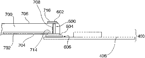
solder which provides the desired solder joint. For example, the solder is
distributed across at least a portion of a surface of a first copper pad 714
coupled to
the first side surface 704 of the PCB 700. For example, with respect to the
first
copper pad 714, the first copper pad 714 has a diameter of 1.4 millimetres,
and
includes an aperture which defines the first opening 710. For example, the
coupling
structure surface interface 606 includes a surface area of at least 125% of
the
surface area of the surface portion of the first copper pad across which the
solder is
distributed.
[0066] In some embodiments, with respect to the retainer 602, the
retainer
602 opposes forces applied to the coupling structure 604 which are normal to
the
coupling structure surface interface 606. For example, the retainer 602
includes
solder which is connected to the PCB 700. For example, the retainer 602
includes
solder distributed across at least a portion of a surface of a second copper
pad 716
coupled to the second side surface 706 of the PCB 700. For example, with
respect
to the second copper pad 716, the second copper pad 716 has a diameter of 1.4
millimetres, and includes an aperture which defines the second opening 712.
[0067] In some embodiments, with respect to the passage 708, the passage
22
CA 02716162 2010-09-30
= 708 includes a diameter of 0.75 millimetres. With further respect to the
passage
708, for example, the passage is defined by a via. In this respect, for
example, the
passage 708 is defined by a plated drill hole, and the first and second copper
pads
= 714, 716 are provided and define the first and second openings 710, 712
to the
passage 708.
[0068] An example embodiment of a method of manufacturing an
example
embodiment of the piezoelectric assembly 400 will now be described. Initially,
an
intermediate assembly, defined by the metal shim (in this example embodiment,
the metal shim is the signal electrode connector 408) supporting and coupled
to an
assembled electrode assembly including the piezoelectric material 406, is
provided.
The flexible PCB 700 is also provided and includes a via which defines the
passage
708 with a plated drill hole 709. The flexible PCB 700 includes the first and
second
copper pads 714, 716 to define the first and second openings 710, 712 to the
passage 708. Solder paste is provided on a surface portion of the first copper
pad
714. The first copper pad 714 is then laser soldered to the metal shim 408 of
the=
intermediate assembly. During the laser soldering, the solder flows through
the =
first opening 710, into the passage 708 defined by the via, and then through
the
second opening 712, becoming radially distributed about the second opening 712
and across the second side surface portion defined by the second copper pad
716.
Upon curing of the solder, the interconnecting structure 600 is formed,
effecting the
coupling of the metal shim 408 to the flexible PCB 700. Also, upon curing, and
as a
necessary incident, the solder extends from the coupling structure interface
606
and into the passage 708. Amongst other things, and without wishing to be
bound
by theory, it is believed that the flowing of the solder through the passage
708
effects a desirable wetting angle for the solder connection between the first
copper
pad 714 and the metal shim 408, which facilitates the formation of a more
robust
mechanical fillet between the first copper pad 714 and the metal shim 408.
[0069] In some embodiments, when exposed to high humidity and high
voltages (e.g., high AC voltages), there is a potential for the electrode
assembly
420 to experience an electrical short failure. This electrical short can be
induced by
23
CA 02716162 2010-09-30
= the migration of conductive material (e.g., silver) through the
piezoelectric material
406 from the first electrode 402 (e.g., a positive electrode) to the second
electrode
404 (e.g., a negative electrode).
[0070] In this respect, and referring to the example embodiment in
FIG.4, in
some embodiments, the signal electrical connector 408 extends over and covers
a
side surface of the first electrode 402, which is opposite to a side surface
of the first
electrode 402 that is disposed in contact engagement with the piezoelectric
material 406 (to thereby effect the electrical communication between the first
electrode 402 and the piezoelectric material 406). For example, the side
surface
over which the signal electrical connector 408 extends over and covers is at
least
50% of the area of the side surface of the first electrode 402 which is
opposite to
the side surface of the first electrode 402 that is disposed in contact
engagement
with the piezoelectric material.
[0071] In some embodiments, the reference electrical connector 410
extends
over and covers a side surface of the second electrode 404, which is opposite
to a
side surface of the second electrode 404 that is disposed in contact
engagement
with the piezoelectric material 406 (to thereby effect the electrical
communication
between the second electrode 404 and the piezoelectric material 406). For
example, the side surface over which the reference electrical connector 410
extends
over and covers is at least 50% of the area of the side surface of the second
electrode 404, which is opposite to the side surface of the second electrode
404
that is disposed in contact engagement with the piezoelectric material.
[0072] In some embodiments, the piezoelectric assembly 400
includes a
spacer 426 positioned about the perimeter of the electrode assembly 420. The
spacer 426 is disposed between the signal and reference electrical connectors
408,
410 such that no electrical communication is provided between the signal
electrical
connector 408 and the reference electrical connector 410 through the spacer
426.
In the example shown, the spacer 426 forms a full ring about the perimeter of
the
electrode assembly 420 and is coupled to the signal and reference electrical
connectors 408, 410 about the full perimeter of the electrode assembly 420. In
the
24
CA 02716162 2010-09-30
= example shown, the spacer 426 is a non-conductive adhesive, such as a non-
conductive adhesive tape, having an inner diameter of about 16mm and an outer
diameter of about 18mm, and is coupled to each of the signal and reference
electrical connectors 408, 410. However, it is contemplated that additional
materials with similar properties and alternative dimensions may be
appropriate. A
suitable non-conductive adhesive tape is 3MTm VHBTM Adhesive Transfer Tape
F9469PC. Thus, the spacer 426, in this example, is an annulus that is larger
than
the electrode assembly 420 but smaller than the signal and reference
electrical
connectors 408, 410. Although the spacer 426 is shown as an annulus, in some
examples, the spacer 426 is not a full annulus, and contains one or more
notches or
gaps.
[0073] In this respect, in some embodiments, the electrode
assembly 420 is
disposed between the signal electrical connector 408, the reference electrical
connector 410 and the spacer 426. In this example, the signal electrical
connector
408, the reference electrical connector 410 and the spacer 426 together define
a
humidity barrier space within which the electrode assembly 420 is disposed.
The
signal and reference electrical connectors 408, 410 and the spacer 426, in
some
examples, are disposed in close contact with each other, forming a humidity
barrier
space with a substantially water-tight seal. This configuration 400 avoids the
need
to provide an additional humidity barrier, such as a silicone conformal
coating,
which in some cases requires increased infrastructure, assembly, time and
overall
cost during manufacturing.
[0074] In some examples, the disposition of the electrode assembly
420
within the humidity barrier space helps to reduce the potential for humidity
to reach
the electrode assembly 420, thus helping to reduce the potential for migration
of
conductive material between the first and second electrodes 402, 404. This
helps to
increase the reliability and performance of the piezoelectric assembly 400.
[0075] In some examples, a signal source 428 is coupled to the
signal
electrical connector 408, such as by laser soldering. Similarly, in some
examples, a
reference source 430 is coupled to the reference electrical connector 420,
such as
CA 02716162 2010-09-30
= by laser soldering, or by being formed integrally with the reference
electrical
connector 410.
[0076] Reference is now made to FIG. 7, showing an exploded
schematic of
another example embodiment of the piezoelectric assembly 400. In this example,
one or both of the signal and reference electrical connectors 408, 410 is
coupled to
the electrode assembly 420 via a conductive adhesive 502.
[0077] In this example, the conductive adhesive 502 is provided
between the
reference electrical connector 410 and the electrode assembly 400. It should
be
understood that in some examples the conductive adhesive 502 can be provided
between the signal electrical connector 408 and the electrode assembly 400, or
between both the signal and reference electrical connectors 408, 410 and the
respective surface of the electrode assembly 400. The conductive adhesive 502
is
designed to be in contact engagement with a portion of the peripheral surface
area
of the first electrode 402, thereby maintaining contact with all portions of
the first
electrode 402, even in the presence of cracking. By peripheral surface area is
meant the surface area of the first electrode 402 that is adjacent or
substantially
adjacent to the periphery of the first electrode 402, and is not necessarily
limited to
surface areas directly adjacent to the periphery of the first electrode 402.
In some
examples, the conductive adhesive 502 is designed with a piezoelectric
material-
accommodating space for accommodating actuation of the piezoelectric material
406. This piezoelectric material-accommodating space has the potential to
reduce
the rigidity of the piezoelectric assembly 400, thus reducing the work
required for
the piezoelectric material 406 to actuate and thereby allowing an increased
response and increased tactile feedback.
[0078] In this example, the conductive adhesive 502 further
includes one or
more surfaces extending inwards from the periphery of the first electrode 402
for
contact engagement with the first electrode 402. In the example shown, the
conductive adhesive 502 includes, for example, four extensions extending
radially
inwards. Such a design has the potential to be useful for increasing the area
of
contact engagement between the conductive adhesive 502 and the first electrode
26
CA 02716162 2010-09-30
= 402. An increased contact engagement area has the potential to improve
electrical
communication between the signal electrical connector 408 and the first
electrode
402. For example, an increased contact engagement area has the potential to
provide a more robust electrical and physical contact.
[0079] Reference is now made to FIG. 8, which is a chart
illustrating the
displacement of an example embodiment of the piezoelectric assembly 400 in
operation. In some examples, the piezoelectric assembly 400 is used as the
tactile
mechanism 39 described above.
[0080] At (1), when the piezoelectric assembly 400, does not
receive a signal,
in some examples there is no electric field generated between the first and
second
electrodes 402, 404, and the piezoelectric material 406 is in its unactuated
state.
The piezoelectric material 406 in this example is concave downwards from the
general plane formed by its peripheral edge such that it is concave away from
the
touch screen display 38, causing a corresponding configuration of the
piezoelectric
assembly 400.
[0081] At (A), in response to an initial touch input at the touch
sensitive
display 38, the piezoelectric assembly 400 receives a signal, for example from
the
processor 22, causing the generation of an electric field between the first
and
second electrodes 402, 404 and a subsequent change of the piezoelectric
material
406 to its actuated state, which in this example brings the piezoelectric
material _
406 (and by extension the piezoelectric assembly 400) to be substantially
planar
with its peripheral edge and substantially flush or in contact with the touch
sensitive
display 38. This change to the actuated state typically occurs gradually
enough to
be unnoticeable by a user, as shown by the gradual rise (B). In this example,
the
piezoelectric assembly 400 exhibits a displacement of about 100 microns over
about 20 ms from the unactuated to the actuated state.
[0082] Over the time period (2), the touch input at the touch
sensitive display
38 exerts further force on the touch sensitive display 38, the force sensed by
the
touch sensitive display 38 increases until a predetermined threshold is
reached at
27
CA 02716162 2010-09-30
= (3) and the touch input is determined to be a full touch input. When the
full touch
= input is determined, the signal to the piezoelectric assembly 400 is
stopped,
causing the dissipation of the generated electric field between the first and
second
electrodes 402, 404 and a subsequent change of the piezoelectric material 406
back to its unactuated state (and by extension the piezoelectric assembly
400),
which in this example is concaved away from the touch sensitive display 38.
The
change back to the unactuated state typically is relatively rapid so that the
user
feels the change, as shown by the sharp drop (C). In this example, the
piezoelectric
assembly 400 exhibits a displacement of about 100 microns over about 3ms from
the actuated to the unactuated state.
[0083] For the duration that the full touch input is maintained on
the touch
sensitive display 38, the piezoelectric assembly 400 remains unactuated. At
(D) the
touch input is removed, and this is sensed by the touch sensitive display 38.
When
the removal of the touch input is determined, a signal is sent to the
piezoelectric
assembly 400, again generating the electric field between the first and second
electrodes 402, 404 and a subsequent change of the piezoelectric element 406
to
its actuated state (and by extension the piezoelectric assembly 400),
substantially
flush with the touch sensitive display 38. Typically, this occurs relatively
rapidly,
such that the change is felt by the user, as shown by the sharp rise (D). In
this
example, the piezoelectric assembly 400 exhibits a displacement of about 100
microns over about 3 ms from the unactuated to the actuated state.
[0084] At (E), the signal to the piezoelectric assembly 400 is
stopped, causing
the generated electric field between the first and second electrodes 402, 404
to
dissipate and thus the return of the piezoelectric material 406 to its
unactuated
state (and by extension the piezoelectric assembly 400). The piezoelectric
assembly
400 typically exhibits a gradual return to the unactuated state, as shown by
the
gradual drop (F). In this example, the piezoelectric assembly 400 gradually
returns
to its unactuated state over about 15ms.
[0085] Thus, in some examples, a user using a touch input on the
touch
sensitive display 38 initially feels a resistance in response to an initial
touch input,
28
CA 02716162 2013-09-04
as the piezoelectric assembly 400 changes to its substantially planar actuated
state.
As the touch input presses further down, the user feels a give or clicking
sensation,
as the piezoelectric assembly 400 returns to its concave unactuated state.
When
the touch input is released, the user feels an upwards clicking sensation, as
the
piezoelectric assembly 400 changes to its actuated state again, before finally
relaxing back to its unactuated state. This behaviour has the potential to be
useful
to provide tactile feedback for the touch screen display 38.
[0086] Although the piezoelectric assembly 400 has been described in
certain
variations and examples, the variations and examples described can be
combined,
and the piezoelectric assembly 400 can have a combination of any of the
variations
described. Although the signal electrical connector 408 is described as
receiving a
signal from a current or voltage source and communicating the signal to the
first
electrode 402, and the reference electrical connector 410 and second electrode
404
are described as being in electrical communication with a reference source,
the
roles signal and reference can be reversed, such that the first electrode 402
is in
electrical communication with the reference source and the second electrode
404 is
in electrical communication with the current or voltage source to receive a
signal.
[0087] In the above description, for purposes of explanation, numerous
details are set forth in order to provide a thorough understanding of the
present
disclosure. However, it will be apparent to one skilled in the art that these
specific
details are not required in order to practice the present disclosure. In other
instances, well-known electrical structures and circuits are shown in block
diagram
form in order not to obscure the present disclosure. Although certain
dimensions
and materials are described for implementing the disclosed example
embodiments,
other suitable dimensions and/or materials can be used within the scope of
this
disclosure. All such modifications and variations, including all suitable
current and
future changes in technology, are believed to be within the sphere and scope
of the
present disclosure.
29