Note: Descriptions are shown in the official language in which they were submitted.
CA 02718423 2010-09-13
WO 2009/114528 PCT/US2009/036666
1
ELECTRONIC BALLAST FOR HIGH INTENSITY DISCHARGE LAMPS
FIELD OF THE INVENTION
This application discloses an electronic ballast device for High Intensity
Discharge (HID) lamps which implements precise control of lamp ignition, lamp
glow-
to-arc currents, and operation of High Intensity Discharge lamps.
BACKGROUND OF THE INVENTION
High Intensity Discharge (HID) lamps are primarily used for large area
illuminations. Unlike an incandescent bulb, a ballast device is necessary to
ignite
and operate an HID lamp. There are three primary functions of a ballast
device,
namely: 1) lamp ignition, 2) lamp power control, and 3) control of AC line
transients
and power quality. Most commonly used HID lamps are high-pressure sodium,
ceramic, and pulse start metal halide lamps. All of these lamps require very
high
voltage for their ignition. Recently, electronic ballasts have been introduced
to
replace the old magnetic ballasts for higher operating efficiency and to
improve lamp
life and lumen maintenance by incorporating controlled ignition and lamp power
regulation schemes.
There are two types of electronic ballasts: ballasts that operate HID lamps
with a frequency that is higher than 20 kHz and ballasts that operate HID
lamps with
a frequency that is lower than 800 Hz. The primary advantage of low frequency
operated electronic ballast is that it doesn't give rise to destructive
acoustic
resonance in the HID lamp. In particular, lower wattage ceramic metal halide
electronic ballasts with a built-in integral igniter are designed to operate
HID lamps at
a low frequency. Although the lamp power regulation is important and offers
other
benefits, it is the proper lamp ignition, controlled glow-to-arc, and arc
stabilizations
that minimize electrode sputtering and ultimately determine the useful life of
an HID
lamp. Various schemes were proposed in the past to achieve these
characteristics,
but they are either too complex or lack completeness.
The starting and operating of an HID lamp involves five stages: two
breakdowns, cold cathode, glow-to-arc transition, and thermionic arc. Prior to
the
CA 02718423 2010-09-13
WO 2009/114528 PCT/US2009/036666
2
initial breakdown, the HID lamp offers very high impedance. Upon application
of a
high voltage across an HID lamp, the induced electric field generates seed
electrons
which cause a breakdown. At the instant of the breakdown, the lamp impedance
drops drastically but almost immediately increases to a higher value as the
HID lamp
enters into a glow discharge phase.
Further, following the breakdown, the HID lamp may enter into either a cold
cathode or glow discharge phase, depending on whether or not mercury in the
HID
lamp has condensed on the electrodes. In order to sustain a glow discharge,
the
voltage across the lamp electrodes attains a higher value, but it is much
lower than
the breakdown voltage. The primary source of electrons during this period is
secondary emission from the lamp electrodes by ion bombardment, which causes
both sputtering and heating of the electrodes. The heating of the lamp
electrodes
raises the cathode temperature sufficiently high for thermionic emission to
occur,
which is the beginning of the glow-to-arc transition. In order to sustain
thermionic
emission, the ballast must supply sufficient current into the HID lamp for
establishing
a conductive arc between the lamp electrodes. Once the arc phase (takeover)
begins, it takes between a few hundred seconds to a few minutes before it
fully
develops.
The starting of an HID lamp and also the associated sputtering of the
electrodes affect the lamp life and the lumen maintenance. In order to
minimize
electrode sputtering during the glow and initial arc phase, balanced and
controlled
transitions are required, which are difficult to incorporate in the design of
magnetic
ballast.
Low frequency electronic ballast operates HID lamps with a frequency that is
usually less than 300 Hz. The lamp operating waveform is an alternating square
wave, which is typically created by a conventional full bridge inverter
circuit. The
square wave operation of the HID lamp yields: a) low lamp current crest
factor, b)
unity lamp power factor, and c) fast polarity transition, which results in
higher
efficiency, lower lamp voltage, and flicker free constant light output.
CA 02718423 2010-09-13
WO 2009/114528 PCT/US2009/036666
3
Low frequency electronic ballasts also primarily utilize two ignition schemes.
These are: a) superimposing a breakdown voltage on top of the low frequency
square wave (which is similar to the ignition scheme of magnetic ballasts) and
b)
high frequency resonant generated ignition pulses. As stated earlier, it is
the quality
of the ignition and transitions that primarily determine useful lamp life and
light
output. Therefore, low frequency electronic ballasts that utilize magnetic
ballast
ignition schemes provide certain improvements but not all that are desired.
Low
frequency electronic ballasts that utilize a controlled high frequency
resonant
scheme for lamp ignitions and then switch to a low frequency for normal
operation
can provide additional improvements.
However, none of the electronic ballasts provide a complete electronic ballast
architecture that ensures proper lamp ignition and operation, since they
typically
address a limited number of aspects of lamp ignition and operation.
BRIEF SUMMARY OF THE INVENTION
The present electronic ballast for High Intensity Discharge (HID) lamps
implements precise control of lamp ignition, lamp glow-to-arc currents, and
the
continued operation of HID lamps. The HID electronic ballast is based on
fundamental HID lamp physics, and implements a complete electronic ballast
architecture that ensures proper lamp ignition and operation.
The present HID electronic lamp ballast uses a "set of controls" that can be
performed by controlling energy delivery by the "line side converter" to the
"lamp side
inverter". This set of controls comprises: 1) open circuit voltage control, 2)
breakdown voltage amplitude control, 3) glow-to-arc transition current
control, 4)
"initial arc development" current control, 5) "arc stabilization" current
control, 6) lamp
power control, 7) lamp dimming, 8) "lamp rectification" current control, and
9) short
circuit and lamp fault protections. One of the primary advantages of this
"line side
converter" energy delivery control method is that it doesn't need to vary the
lamp
operating frequency to achieve the above-noted controls.
The HID electronic lamp ballast also divides the arc development period into
two sections, namely, 1) the "initial arc development" period, which begins as
soon
CA 02718423 2010-09-13
WO 2009/114528 PCT/US2009/036666
4
as the lamp enters into the arc phase and thereafter lasts a period of
preferably not
less than 1 second, and 2) the "arc stabilization" period, which follows the
"intermediate arc development" period and continues until the lamp reaches a
normal operating state.
Thus, the present HID electronic lamp ballast provides a complete electronic
ballast architecture that ensures proper lamp ignition and operation since it
is based
on fundamental HID lamp physics and generally available lamp data.
BRIEF DESCRIPTION OF THE DRAWINGS
Figure 1 illustrates an embodiment of the present electronic ballast for High
Intensity Discharge (HID) lamps which implements precise control of lamp
ignition,
lamp glow-to-arc currents, and operation of HID lamps;
Figure 2 illustrates the typical starting and operating impedance
characteristics of an HID lamp;
Figure 3 is a flow chart that describes the "design guide" sequential control
functions;
Figure 4 illustrates the DC bus voltage that appears across an HID lamp
during the breakdown and until the lamp enters into a stable operating mode;
Figure 5 illustrates a graph of the ignition voltage profile of an HID lamp;
Figure 6 illustrates a graph of the ignition voltage profile of an HID lamp;
Figure 7 illustrates, in block diagram form, the typical architecture of
electronic
ballast, which is powered by an AC source;
Figure 8 illustrates, in block diagram form, the typical architecture of
electronic
ballast, which is powered by a DC source;
Figure 9A illustrates a lamp inverter circuit that is based on conventional
half
bridge topology;
CA 02718423 2010-09-13
WO 2009/114528 PCT/US2009/036666
Figure 9B illustrates a lamp inverter circuit that is based upon conventional
full
bridge topology;
Figure 9C is a variation of Figure 9B which illustrates the use of a split
inductor in this lamp inverter circuit;
5 Figure 10A illustrates a single stage power converter;
Figure 10B illustrates a more detailed version of the full bridge inverter
circuit
of Figure 9B;
Figure 10C illustrates an electronic ballast that is based on a single stage
"line
side converter" topology;
Figure 11A illustrates a variation of Figure 1, whereby an inductor L2 is
connected between the diode D1 and D2;
Figure 11 B illustrates a variation of Figure 11A, whereby a series connected
diode D13 and a resistor Ra are added between D2 anode and D8 cathode for
delivering additional charging current during the lamp breakdown voltage
generation;
Figure 12 describes the half bridge control circuit SC1 of Figure 1; and
Figure 13 discloses the "lamp side inverter" control circuit SC2 of Figure 1.
DETAILED DESCRIPTION OF THE INVENTION
High Intensity Discharge (HID) lamps are primarily used for large area
illuminations. Unlike an incandescent bulb, a ballast device is necessary to
ignite
and operate an HID lamp. There are three primary functions of a ballast
device,
namely: 1) lamp ignition, 2) lamp power control, and 3) control of AC line
transients
and power quality. HID lamps have negative resistance characteristics. Because
of
these physical characteristics, all gas discharge lamps are current
controlled.
However, even by maintaining a constant current in the lamp, lamp power cannot
be
controlled over the life of the lamp because the lamp voltage typically
increases over
the life of the lamp. Therefore, complex electronic ballast circuits are
required for the
proper ignition, control, and operation of HID lamps.
CA 02718423 2010-09-13
WO 2009/114528 PCT/US2009/036666
6
Basic Architecture Of Electronic Ballast
Figure 7 illustrates, in block diagram form, the typical architecture of
electronic
ballast, which is powered by AC source, while Figure 8 illustrates, in block
diagram
form, the typical architecture of electronic ballast, which is powered by a DC
source.
In Figure 7, element A of the electronic ballast receives alternating line
power
and incorporates conventional input power regulation circuit such as fusing,
AC line
transient protection, and EMI filters (DG12). The element A is termed the "AC
front
end" circuit. The element B of the electronic ballast is a conventional full
bridge
rectifier for rectifying the alternating line voltage into DC sinusoids. The
element C of
the electronic ballast is for power factor corrections and total harmonic
distortion
reductions (DG12) and employs, for example, a conventional boost type
converter
circuit. The element D of the electronic ballast is a DC-DC converter and
employs,
for example, a conventional buck type circuit. The voltage that appears at the
input
of element D is labeled DC1, and the DC voltage that appears at the input of
element
E is labeled DC2. The element E of the electronic ballast employs a DC-AC
inverter
circuit for creating ignition pulses and also for providing alternative power
to an HID
lamp during its normal operation. The control circuits CO1, C02, and C03 are
the
respective control circuits for element C, element D, and element E of the
electronic
ballast. Further, elements A, B, C, and D, and control circuits CO1 and C02
combined are termed the "line side converter" herein. Further, element E and
its
control circuit C03 combined are termed "lamp side inverter" herein. The
architecture of Figure 7 represents the generalized building blocks of a
typical AC
powered electronic ballast. The DC-AC inverter circuit of element E in Figure
7 is
commonly based on half or full bridge topology.
Basic Characteristics Of High Intensity Discharge (HID) Lamps
The physics of the HID lamps are very complex. The primary focus of most
existing electronic ballasts is to improve the electronic ballast circuit
exclusively for
cost savings. In addition, although major lamp manufacturers often emphasize
lamp
ballast optimizations, it is difficult to find a complete set of lamp physics
data for a
specific HID lamp. The HID lamp data that are generally available are: a) lamp
type,
b) lamp ignition voltage, c) lamp wattage, and d) lamp voltage. It is one of
the goals
CA 02718423 2010-09-13
WO 2009/114528 PCT/US2009/036666
7
of the present HID electronic lamp ballast to operate the HID lamp based on
fundamental HID lamp physics and generally available lamp data.
The typical starting and operating impedance characteristics of an HID lamp
are shown in Figure 2. In order to better understand the present HID
electronic lamp
ballast, the starting sequence of an HID lamp in relation to these impedance
characteristics is described herein.
HID lamps produce light by striking an electrical arc across metal electrodes
housed inside a specially designed inner fused quartz or fused alumina tube.
This
tube is filled with both gas and metals, where the gas aids in the starting of
the
lamps. The metals then produce the light once they are heated to a point of
evaporation, forming a plasma inside the tube. In all HID lamps, light is
produced by
passing a current through a metal vapor. Free electrons colliding with an atom
in the
metal vapor momentarily knock an electron into a higher orbit of the atom.
When the
displaced electron falls back to its former level, a quantum of radiation is
emitted.
The wavelength of radiation depends on the energy zone of the disturbed
electron
and on the type of metal vapor used in the arc tube. Although it produces 5%
of its
output when first ignited, the HID light requires a few seconds (usually 15-
20) to
come up to full output. Also, if power to the lamp is lost or turned off, the
arc tube
must cool to a given temperature before the arc can be re-struck and light
produced.
The ballast in an HID lighting system generally has two purposes. It provides
the
proper starting voltage to strike and maintain the arc, and it regulates the
proper
current to the lamp once the arc is established.
Ballasts are not often interchangeable among different types of HID lamps. A
ballast design incorporates an electronic circuit to provide specific
lamp/ballast
operating characteristics. As an example, the effects of line voltage
variations on
resultant changes of lamp wattage are a function of the ballast circuit
design.
Requirements for a circuit which provides a finer degree of lamp regulation
generally
result in a higher ballast cost.
High Intensity Discharge (HID) Lamp Breakdown On Ignition
CA 02718423 2010-09-13
WO 2009/114528 PCT/US2009/036666
8
At the instant of the lamp breakdown, the lamp impedance can be less than 1
ohm for a very short period of time, as indicated by point B1 in Figure 2.
This low
lamp impedance creates almost a short circuit condition; therefore, an
electronic
ballast control circuit must limit current into the HID lamp. Following the
lamp
breakdown, the impedance almost immediately goes back to a much higher value,
causing the lamp voltage to rise, as indicated by point G1 in Figure 2. It is
desirable
to produce control voltages that result in a short glow state duration, a low
glow state
current, as well as a high glow state lamp voltage in order to minimize
electrode
sputtering. Following the glow period, the lamp enters into the arc
development
phase.
Although a controlled glow-to-arc transition reduces electrode sputtering,
this
gets further complicated when a low frequency HID electronic ballast employs
high
frequency ignition pulses for the lamp breakdown, which switches to the low
operating frequency following the lamp ignition. This switching often creates
additional problems, such as extinction and excessive and asymmetrical current
draw. In order to overcome these problems, the present HID electronic lamp
ballast
divides the arc development period into two sections, namely, 1) the "initial
arc
development" period, which begins as soon as the lamp enters into the arc
phase
and thereafter lasts a period of preferably not less than 1 second, as
indicated by
point All in Figure 2, and 2) the "arc stabilization" period, which follows
the
"intermediate arc development" period and continues until the lamp reaches a
normal operating state as indicated by point AS1 in Figure 2.
It must also be noted that the impedance characteristics, as illustrated in
Figure 2, is a generalized behavior of an HID lamp. The actual values are not
only
time dependent but can also change depending on many variables such as the
cold
lamp start vs. hot re-ignition, lamp-to-lamp variations, and lamp aging.
Design Criteria For A Low Frequency Electronic High Intensity Discharge (HID)
Ballast
The primary goal of the present HID electronic lamp ballast is to implement a
complete architecture for low frequency electronic HID ballast. Accordingly,
the first
CA 02718423 2010-09-13
WO 2009/114528 PCT/US2009/036666
9
aspect of this HID electronic lamp ballast uses a "design guide" consisting of
twelve
distinct design criteria (DG), comprising:
DG1: Open Circuit Voltage: The ballast shall supply an open
circuit voltage of at least 280V to an HID lamp. This open circuit voltage is
necessary for generating required breakdown pulses; also upon
breakdown and before the lamp enters into an arc state, the high open
circuit voltage creates a favorable condition for glow to arc transition.
DG2: Breakdown Voltage:The ballast provides periodic high
frequency breakdown voltage pulses to an HID lamp in a manner that
causes the lamp to breakdown at a lower voltage, which reduces
sputtering of cathode materials.
DG3: Breakdown Voltage Limit: The ballast limits the magnitude
of the breakdown voltage. Unless hot re-ignition is required, the
breakdown voltage shall not be more than 3,500V.
DG4: Glow-To-Arc Transition: The ballast minimizes the
transition time and the lamp current flow during the glow-to-arc phase
transition. Prior to entering into the arc phase, the lamp impedance
remains high. A prolonged glow state duration and uncontrolled current
into the lamp increases electrode sputtering.
DG5: "Initial Arc Development" Current: As the HID lamp enters
into the beginning phase of the arc, the ballast provides a controlled
current into the lamp for a period of preferably no less than one second.
The controlled current is higher than the glow-to-arc state current but
lower than the "arc stabilization" current. These thresholds minimize
cathode sputtering, while also preparing the lamp for a smooth transition
to the low operating frequency. A smooth transition herein is defined as a
transition that prevents lamp extinction and excessive and asymmetrical
current drawn.
DG6: High Frequency To Low Frequency Transition: Prior to
switching to the low operating frequency, the ballast increases the arc
CA 02718423 2010-09-13
WO 2009/114528 PCT/US2009/036666
current to a level that is higher than the "initial arc development" current
but not more than two times the normal operating current. This ensures a
smooth transition from a high operating frequency to the low operating
frequency.
5 DG7: "Arc Stabilization" Current: As the lamp switches to the low
operating frequency, the ballast limits the "arc stabilization" current not to
exceed twice the lamp normal operating current.
DG8: "Lamp Rectification": The ballast incorporates a circuit
that avoids or limits asymmetrical current drawn in an HID lamp. During
10 the transition from high frequency to low frequency, during the "arc
stabilization period", as well as during the normal lamp operation, the lamp
may enter into a state which is commonly known as "lamp rectification"
state. Prolonged lamp operation in a rectification state may cause both
ballast failures and lamp ruptures.
DG9: Lamp Power Control: Following the "arc stabilization"
period, the ballast maintains a specified power into an HID lamp during the
normal operation. The operating impedances of HID lamps, in particular
high-pressure sodium lamps, change substantially over their lives.
Therefore, an electronic ballast must incorporate a power control circuit for
maintaining the specified lamp wattage.
DG10: Fast Polarity Transition: The ballast operates an HID lamp
such that during the normal operating state, the AC square wave switches
its polarity very quickly. The combination of the square wave operation of
an HID lamp and the very fast transition from positive to negative voltage
polarities not only ensures low lamp current crest factor, unity lamp power
factor, minimum operating voltage and current overshoot, and
substantially constant light output, but also increases lamp life and
efficiency.
DG 11: Short Circuit And Lamp Fault Protection: The ballast
withstands output short circuit conditions and protects against abnormal
lamp operations.
CA 02718423 2010-09-13
WO 2009/114528 PCT/US2009/036666
11
DG12: AC Line Power Quality Maintenance: The ballast draws
power from an AC line in a manner to limit turn-on inrush current, provide
transient protections, limit electromagnetic interference, provide high
power factor, and reduce total harmonic distortions.
While a few of the above design criteria are known, in order to combine the
lamp physics characteristics with efficient power conversion, all twelve of
the design
criteria need to be incorporated in an HID electronic ballast circuit.
Electronic Ballast Circuits
Figure 9A is a typical lamp inverter circuit that is based on conventional
full
bridge topology. The circuit elements Sa, Sb, Sc, and Sd are power switches,
and L
is an inductor, which is connected in series with a capacitor C. The load is
an HID
lamp RL, which is connected across capacitor C. Figure 9B is a variation of
Figure
9A whereby the inductor L of Figure 9A is split into two inductors La and Lb.
The
series combination of the inductor L and the capacitor C creates the lamp
breakdown
voltage by changing the operating frequency of the full bridge inverter to the
natural
series resonant frequency of inductor L and capacitor C. The values of
inductor L
and capacitor C are usually kept low in order to minimize the circulating
current into
the resonant tank. Further, the lower the value of capacitor C, the lower the
capacitive effects during the normal operation of the lamp.
There are various ways the "design guide" implementations can be realized in
an electronic ballast. However, a few design criteria such as AC inrush
current
limiting (DG12), short circuit, and lamp fault protections (DG11 and DG12) may
be
inherent to certain power conversion topologies. These inherent properties
simplify
the implementation of the "design guide" in an electronic ballast. US
Published
Patent Application No. 11/375,558 combines the element C and the element D of
Figure 7 into one element whereby the power factor corrections (DG12) and DC-
DC
conversions are accomplished in a single stage. An illustration of such a
single
stage power converter is shown in Figure 10A, which corresponds to the Figure
7 of
the US Published Patent Application No. 11/375,558. The primary advantages of
a
single stage power conversion are: 1) high power conversion efficiency, 2)
less
number of components, 3) inherent turn-on AC inrush limit, 4) low stress short
circuit,
CA 02718423 2010-09-13
WO 2009/114528 PCT/US2009/036666
12
and 5) lamp fault protections. The additional benefits of single stage power
conversion are further evident in the following description.
In Figure 10A, the rectifiers R rectify the AC power. Capacitor C1 is a small
high frequency filter capacitor. It is well known that during power
conversions high
frequency noise is generated by power component switching actions within the
device. The purpose of diode D1 is to prevent high frequency switching related
circuit noise from conducting back to the AC line. The pair of power switches
S1 and
S2 is connected across the input lines and switch alternately. The switching
speed
and on and off time periods are usually controlled by an integrated control
circuit SC.
The capacitor C4 is a large smoothing electrolytic capacitor. The diodes Dx
and Dy
are commutating diodes. The resistor RS1 is a current sense resistor. When an
inductor LR and the capacitor CR are placed as shown in Figure 10A, and when
the
switching frequency f is such that f = 1 /2rr'l(LR x CR), they form a resonant
tank
circuit. The diodes D4, D5, D6, and D7 are a full bridge high frequency
rectifier that
provides additional DC power to the load RL. The capacitor C6 is a high
frequency
filter capacitor for the output load. The value of this high frequency filter
capacitor
C6 may be as low as 1 uF for a 250W High Pressure Sodium (HPS) lamp ballast
inverter, for example. The capacitor C5 is also a small capacitor such as 0.1
uF. On
the other hand, depending on the magnitude of the output load, the value of
the
smoothing capacitor C4 may be greater than 100 uF. Capacitor CB is a DC
blocking
capacitor. Resistor RS1 is a current sensing resistor.
Assuming the value of capacitor C5 is 1 uF, and because it is connected in
series with smoothing capacitor C4, a much larger value capacitor whose value
may
be higher than 100 uF, the effective series capacitance of capacitors C4 and
C5 is
less than 1 uF. Therefore, immediately following the application of the input
AC
power to the circuit of Figure 1 OA, the charging current that flows from the
AC line
into the smoothing capacitor C4 is lower, and its duration is significantly
shorter
simply because the input AC power source sees a much smaller capacitor as
opposed to a much larger value smoothing capacitor C4. Therefore, the control
circuit maintains the AC inrush current of short duration, and low magnitude
at turn
on is due to the fact that the input AC power source sees a small capacitor.
CA 02718423 2010-09-13
WO 2009/114528 PCT/US2009/036666
13
Auxiliary High Frequency AC Voltage Source
Further, the resonant inductor LR has a secondary winding W1. The voltage
that is generated across winding W1 is high frequency AC. A voltage of
magnitude
of 1:5 with respect to the input AC line voltage peak value is sufficient. The
high
frequency AC voltage across winding W1 is rectified by a diode D10 to produce
an
auxiliary source of DC power for the load RL. This rectified DC voltage Vaux
is
smoothed out by a smoothing capacitor C7 and then fed back at the junction of
diodes D1 and D2. Further, the rectified voltage Vaux also can be obtained by
a full
bridge rectifier arrangement, or this voltage can be fed at the junction of
diodes D4
and D5. It must be understood that within the power conversion device this
auxiliary
DC power source also can be created by other means such as use of a low power
conventional buck converter. However, creating this power source from the
winding
W1 is certainly straightforward and cheaper. The auxiliary high frequency AC
voltage source is used to produce the auxiliary DC power Vaux which is used in
the
present improved single stage power converter for the reduction of output
ripples. It
must be noted that the output ripples also can be reduced by controlling the
operating frequency of the "line side converter" at or near the 50/60 Hz AC
zero-
crosses.
The reduction of output ripples by the use of the auxiliary DC supply Vaux is
explained as follows. Near the zero crossings of the input line AC voltage,
the
rectified DC sinusoids produced by rectifier R approach zero potential and
cannot
provide the required energy to the load RL. As a result, the resonant inductor
LR,
near the zero crossing of the input line AC voltage, tries to extract energy
out of a
very low voltage source, which causes certain overshoots. Therefore, the
voltage
that develops across the resonant capacitor CR also experiences certain
overshoots.
These overshoots inject a power ripple into the load RL at the rate of 120 Hz
for
60Hz AC input and at the rate of 100 Hz for 50 Hz AC input. Therefore, the DC
power source Vaux, when connected as shown in Figures 10A, acts as a secondary
power source near zero crossings of the input line AC voltage.
In operation, the capacitor C7 gets fully charged rapidly near the peak of the
DC sinusoids and delivers power to the load RL when the rectified DC sinusoid
CA 02718423 2010-09-13
WO 2009/114528 PCT/US2009/036666
14
voltage drops below the value of Vaux. The benefits of this auxiliary DC power
source are substantial. First, in AC applications when a load RL is connected
directly across the resonant capacitor CR and powered by high frequency, the
voltage ripples near zero crossings are substantially reduced. This eliminates
power
variation and flickering into the load RL near zero crossings of the input
line AC
voltage. Second, in DC applications, due to reduced ripples, the value of the
output
filter capacitor C6 can be substantially smaller. Therefore, in many
applications, film
capacitors may be used. Good quality film capacitors have longer life and much
lower loss compared to electrolytic capacitors. Therefore, this increases
device
reliability and power conversion efficiency. Further, the use of a low value
filter
capacitor results in a faster response time for output load regulation. Third,
when
power switches S1 and S2 switch near zero crossings of the AC voltage present
on
the input lines, the power switches S1 and S2 experience additional switching
noise.
The application of Vaux not only reduces the switching noise but also improves
overall Power Factor and Total Harmonic Distortion. Further, the application
of Vaux
also adds the overall output power delivery capacity by 4% to 5%.
Inrush Current Flow Limitation
During the normal operation, when switch S2 closes, energy flows into switch
S2 through resonant inductor LR, capacitor CB, as well as diode D1 and
resonant
capacitor CR, through diode D4, load RL, and diode D6. However, as energy
flows,
primarily the load current that flows through diode D1, load RL, and diode D5
reaches the junction of the diodes D6 and D8, part of this energy also flows
into
smoothing capacitor C5 and thereby charges the smoothing capacitor C5. The
voltage that is generated between the capacitors CR and CB with respect to
circuit
ground (lead DC2) is high frequency AC. Therefore, the diodes D4, D5, D6, and
D7
act as a bridge rectifier. The DC voltage that appears across the junctions D4-
D5 is
plus and D7-D6 is minus.
The charging current into smoothing capacitor C5 primarily depends on the
impedance of the load RL, since the lower the impedance the higher the
charging
current. During a no load situation, the current flow into smoothing capacitor
C5
reduces almost to zero. The diode D8 prevents charging smoothing capacitor C5
CA 02718423 2010-09-13
WO 2009/114528 PCT/US2009/036666
directly from the AC line; however, once smoothing capacitor C5 is fully
charged, it
acts as a smoothing capacitor.
Circuit Characteristics Of The Improved Single Stage Power Converter
Because it is evident to anyone skilled in the art, the following are stated
in
5 reference to Figure 10A:
1. For a power conversion device that requires delivering low power to
the output load, one or all of the diodes D3, D4, and D7 can be
eliminated.
2. High frequency bypass capacitors as snubber or for energy transfer
10 optimization may be added across any or each of the diodes D1
through D8, including one or more diodes may be replaced by the
capacitors.
3. The power switches S1 and S2 are part of a half bridge resonant
inverter. A conventional full bridge resonant inverter can also be
15 constructed and used for the delivery of higher output power.
Further, a transformer in these inverters also can be added for
output load isolation.
4. Non-resonant and quasi-resonant circuits based on other
topologies such as fly back topology may also be used.
5. The output power into the load can be regulated by such
conventional techniques as Pulse Width Modulation (PWM) or by
frequency modulation. Therefore, actual operating frequency may
be different than resonant frequency.
6. The diode D1 may be replaced by an inductor; however, the cost of
an inductor is much more than a diode.
7. The resonant inductor LR and the resonant capacitor CR
connections in Figure 1 OA may also be connected and rearranged
in various manners. Each of these alternatives may appear
substantially different than the circuit arrangement of Figure 1 OA.
CA 02718423 2010-09-13
WO 2009/114528 PCT/US2009/036666
16
However, circuit analysis shows that various arrangements within
the topology under the present improved single stage power
converter yields the same circuit functions either at the expense of
additional components or power conversion efficiency.
Full Bridge Inverter Circuit
Figure 1 OB, which corresponds to the Figure 20 of the US Published Patent
Application No. 11/375,558, is a more detailed version of the full bridge
inverter
circuit of Figure 9B. The switches S3 and S5 form one pair, and the switches
S4 and
S6 form the other pair of a full bridge inverter. It is important to note that
the low
frequency excited HID ballast operating frequency range usually lies between
50 Hz
and 300 Hz. The switching control circuit SC2 is a conventional switched mode
IC
and generates alternate low frequency drive signals at the output terminals A
and B.
There are other known techniques to provide low frequency drive signals, but
one
convenient way to provide low frequency drive signals to respective switch
pairs of a
full bridge inverter is by means of a commercially available high and low side
driver
IC. The first device, IC1, is responsive to the drive signal that arrives at
the terminal
A and drives the switch pair S3 and S5. In Figure 1 OB, IC1 I signifies the
low-side
drive section of IC1, and IC1 h signifies the high-side drive section of IC1.
Further,
the second device, IC2, is responsive to the drive signal that arrives at the
terminal B
and drives the other switch pair S4 and S6. In Figure 20, IC21 signifies the
low-side
drive section of IC2, and IC2h signifies the high-side drive section of IC2.
Further, the switches S3, S4, S5, and S6 may be bipolar, IGBT, or power
MOSFET types of devices. However, the preferred choice is power MOSFET
devices. This is because of the following advantages: a) during the normal
operation, the operating frequency is low; therefore, the body diodes of the
MOSFET
devices can be used as the full bridge commutating diodes; b) low on
resistance
MOSFET devices yield higher power conversion efficiency; and c) during
ignition
period, the operating frequency is much higher. MOSFET devices are also easier
to
turn on and turn off at higher frequency.
Further, the purpose of the inductor Lo and the capacitor Co are explained as
follows. HID lamps, and in particular HPS lamps, require in excess of 3000V
for
CA 02718423 2010-09-13
WO 2009/114528 PCT/US2009/036666
17
ignition. Therefore, at the beginning, the switching control circuit SC2 can
be
programmed to operate at a sweeping frequency with periodic intervals for
generating high voltage ignition pulses by resonant and harmonic resonant
means.
Electronic Ballast Using A Single Stage "Line Side Converter" Topology
Further, Figure 10C is a combination of the "AC front end" circuit of Figure
7,
the circuit of Figure 10A, and the circuit of Figure 10B; together they
constitute an
electronic ballast that are based on a single stage "line side converter"
topology.
The circuit of Figure 10C performs the following primary functions: a)
inherently limits
turn-on AC inrush (DG12), b) provides power factor corrections (DG12) and DC-
DC
conversion in a single stage, c) generates a controlled high frequency
breakdown
voltage (DG2 and DG3), and d) operates an HID lamp with low frequency square
wave.
A brief explanation of the circuit and functions of the various circuit
components in Figure 10C are as follows. The fuse F1, the inductors L1A and L1
B,
the metal oxide varistor VR, the capacitors C1, C, C3, and C4 together form an
"AC
front end" circuit. The power switches S1 and S2, the resonant inductor LR1,
the DC
blocking capacitor CB, resonant capacitor CR1, and the power factor correction
capacitor CP are all part of a half bridge resonant circuit. The half bridge
control
circuit SC1 consists of various circuits including a switch mode IC for
generating
drive signals for the power switches S1 and S2. The high side switch S1 drives
are
isolated by such devices as pulse transformers or level shifting devices. BR1
is a full
bridge AC line rectifier. The diodes D1, D2, and D3 are for channeling
rectified AC
sinusoids and resonant energy. The diodes D4, D5, D6, and D7 are part of a
full
bridge rectifier for rectifying high frequency voltage and current that
appears across
the resonant capacitor CR. The capacitor C9 filters high frequency contents.
The
diode D8 provides high frequency charging current to the storage capacitor C6.
The
diode D9 has two functions, namely, delivers energy from C6 to the switch S1
and
also prevents charging C6 by the rectified AC sinusoids, thereby limiting AC
inrush.
DCH1 is the positive DC bus voltage that is fed to the half bridge inverter.
DCH2 is
the negative side of the DC bus voltage and commonly termed as the power
ground.
The diode D10 rectifies voltage that appears across the secondary winding W1
and
CA 02718423 2010-09-13
WO 2009/114528 PCT/US2009/036666
18
stores energy into the capacitor C7. The diode D11 channels this energy into
the
junction of the diodes D1 and D2 for the purpose of minimizing switching
transients
at the AC zero crossings. The capacitors C5 and C8 are small value capacitors
for
bypassing high frequency switching contents.
The voltage that appears across the capacitor C9 is fed to the full bridge
inverter of the power switches S3, S4, S5, and S6, where DCF1 is the positive
polarity and DCF2 is the negative polarity of this voltage. The control
circuit SC2
consists of various circuits including a switch mode IC that generates drive
signals
for the full bridge power switches. IC1 H and IC2H are isolated high side
drivers.
IC1 L and IC2L are low side drivers. Alternatively, the switch mode IC and
these four
discrete drivers can be replaced by a single self-oscillating full bridge
driver IC. The
inductor LR2 and the capacitor CR2 form a resonant tank circuit for the
purpose of
generating the breakdown voltage. The load RL is an HID lamp.
The lamp power control (DG9) may be accomplished by means of sensing the
lamp current and the DC bus voltage DCF1. There are many ways the lamp current
can be sensed, but a high frequency current transformer means is
straightforward
and less sensitive to circuit noise. In Figure 6C, a current transformer CT is
placed
in the input of the high frequency bridge rectifier diodes D4, D5, D6, and D7.
Further, the filter capacitor C9 is a low value capacitor, usually 1
microfarad. Due to
its low value, this filter capacitor does not interfere with the lamp current
detections
by high frequency means. It must be noted that the high frequency current that
powers the lamp drive circuit in Figure 6C is bi-directional, whereas, a "line
side
converter" that is based on a boost-buck topology delivers a high frequency
current
in only one direction, which makes lamp current sensing by a current
transformer
very difficult. Although the lamp current can be sensed by placing a current
transformer in one of the legs of the lamp, this requires a current
transformer that
can sense low frequency current during the normal operation. A low frequency
current transformer is expensive and, depending on the response
characteristics,
may not sense properly the high frequency current during the glow-to-arc
period.
Further, a scaled sum of the lamp voltage DCF1 and the lamp current may be
applied to a comparator for controlling the lamp power by varying either the
duty
CA 02718423 2010-09-13
WO 2009/114528 PCT/US2009/036666
19
cycle or operating frequency of the "line side converter" of Figure 1 OC. A
detailed
discussion on this subject can be found in US Patent No. 7,199,528.
Additional Electronic Ballast Using A Single Stage "Line Side Converter"
Topology
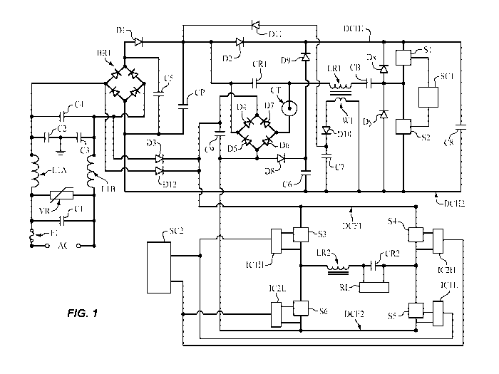
Figure 1 is a variation of Figure 10C, whereby two diodes D3 and D12 directly
connect the AC lines to DCF1. This circuit arrangement bypasses the diode D1
and
thereby further improves power conversion efficiency. Figure 11A is a
variation of
Figure 1, whereby an inductor L2 is connected between the diode D1 and D2.
This
arrangement further improves the AC line total harmonic distortions. Figure 11
B is a
variation of Figure 11A, whereby a series connected diode D13 and a resistor
Ra are
added between D2 anode and D8 cathode for delivering additional charging
current
during the lamp breakdown voltage generation.
The circuits of Figures 1, 11A, and 11 B utilize a half bridge inverter for
single
stage power conversions. Nonetheless, without deviating from the scope of this
HID
electronic lamp ballast, single stage power conversions can also be achieved
by
using such popular switch mode topologies as full bridge, fly-back, push-pull,
and
forward converter topologies.
For the purpose of the following description, the circuit of Figure 1 is used
as
an example. The HID electronic lamp ballast uses a "set of controls" which can
control energy delivery by the "line side converter" to the "lamp side
inverter". These
are: 1) open circuit voltage control, 2) breakdown voltage amplitude control,
3) glow-
to-arc transition current control, 4) "initial arc development" current
control, 5) "arc
stabilization" current control, 6) lamp power control, 7) lamp dimming, 8)
"lamp
rectification" current control, and 9) short circuit and lamp fault
protections. One of
the primary advantages of this "line side converter" energy delivery control
method is
that it doesn't need to vary the lamp operating frequency to achieve the above
control, in particular, during the glow-to-arc transition state. This is
further explained
as follows.
Following a lamp breakdown, the most critical transitional states where an
HID lamp may suffer substantial electrode sputtering, extinction, and "lamp
rectification" are the glow, glow-to-arc, and high frequency to low frequency
transition
CA 02718423 2010-09-13
WO 2009/114528 PCT/US2009/036666
states. Further, for HID electronic ballasts that employ a frequency sweep
method
for the lamp ignition, the operating frequency continues to decrease following
a
breakdown while the lamp impedance experiences dynamic changes. These
conditions create difficult challenges for lamp current control that require
5 simultaneous monitoring of the lamp voltage, the lamp current, and the lamp
frequency, or a combination thereof. The lamp voltage and the lamp frequency
are
not only difficult to monitor during the glow-to-arc transition but, as stated
earlier,
they also change depending on the cold lamp start vs. hot re-ignition, lamp-to-
lamp
variations, and lamp aging. US Patent No. 6,160,362 teaches an arc current
control
10 scheme that is based on the lamp operating frequency variations in steps.
The arc
current control means by lamp operating frequency variations in multiple
steps, while
the frequency was already varying following a breakdown, and that the lamp
impedance characteristics do not remain constant, are not only complex but
also
difficult to implement with precisions, in particular, during the glow-to-arc
transition
15 periods.
Further, US Patent No. 7,187,136 teaches monitoring both the lamp voltage
and the lamp current, which are then compared with predetermined set values in
a
microprocessor for controlling the lamp power by controlling the current
output of a
boost-fly back type "line side converter". As stated earlier, it is difficult
to monitor the
20 lamp voltage during the arc-to-glow periods, but also it can vary depending
on the
lamp brand and operating conditions. Further, this method of the lamp current
control cannot distinguish between the glow-to-arc stabilization current and
the "lamp
rectification current", which is explained in more details in the following
disclosures.
Line Side Converter Energy Delivery Control
The "line side converter" energy delivery control scheme of the HID electronic
lamp ballast requires only to sense the lamp current and not the lamp
frequency or
the lamp voltage for controlling the lamp current, in particular, during the
glow-to-arc
phase. This simplifies feedback control loops and, therefore, yields higher
accuracy
and stability. A "line side converter" that is based on the single stage power
conversion circuit of Figure 1 offers an additional benefit. This is explained
as
follows. During the glow-to-arc transition period, as well as during the arc
CA 02718423 2010-09-13
WO 2009/114528 PCT/US2009/036666
21
development, the lamp impedances vary constantly, including almost creating a
short circuit condition. These dynamic lamp impedance changes often require a
fast
sensing type feedback control scheme to prevent momentary large arc current
flowing into the lamp. These are very difficult to achieve in a boost-buck
based
electronic ballast. On the other hand, in Figure 1, the load output of a
single stage
resonant converter inherently behaves like a very fast acting impedance power
source. This fast acting impedance power source, which supplies power to the
lamp
inverter, combined with the lamp current feedback can control the arc current
on a
real time basis with precision. Further, this fast acting impedance power
source
property not only assists in controlling the arc current into the lamp but
also assists in
maintaining the required amount of the open circuit voltage when it is
required and
as demanded by the lamp for sustaining the glow discharge. In other words,
this
particular property of the "line side converter" assists in creating a
favorable
condition for the lamp whereby the electronic ballast circuitries and feedback
controls
follow the time dependent glow-to-arc characteristics of an HID lamp but not
the
other way around.
Control And Implementation Of High Intensity Discharge Electronic Lamp Ballast
The following disclosures are the foundations of the control and
implementation schemes under this HID electronic lamp ballast. The graph DCF1
in
Figure 4 shows the DC bus voltage that appears across an HID lamp during the
breakdown and until the lamp enters into a stable operating mode. The graphs
FL
and IL in Figure 4 are the corresponding lamp operating frequency and the lamp
current. The lamp voltage, the lamp current, and the frequency values that are
shown in Figure 4 are normalized for illustrations. The arrows al, a2, and a3
indicate the voltage, lamp current, and operating frequency prior to
generating the
breakdown voltage, respectively. This frequency is set approximately at 250
kHz.
The arrows b1, b2, and b3 indicate the voltage, lamp current and, operating
frequency, respectively, when the lamp enters into a glow state following a
breakdown. The voltage b1 is set approximately at 290V.
The arrow LB shows that, prior to entering into the glow state and at the
instant of the breakdown, the voltage across the lamp drops for a short
duration,
CA 02718423 2010-09-13
WO 2009/114528 PCT/US2009/036666
22
which corresponds to the impedance drop 131 in Figure 2. The arrows c1, c2,
and c3
indicate the voltage, lamp current, and operating frequency, respectively,
during the
"initial arc development" period. This voltage c1 is approximately 50V. The
current
c1 is set at a higher level than the glow state current and approximately
corresponds
to lamp normal operating current. The operating frequency settles to an
intermediate
frequency, "Fl", and it is usually set at approximately 6 kHz. It can be
noticed that
the difference between the glow state voltage b1 and the "initial arc
development"
voltage is approximately 240V. Therefore, this sharp voltage drop may be used
for
detecting the transition between the glow state and the "initial arc
development"
state. The arrows e1, e2, and e3 indicate the voltage, lamp current, and the
frequency at the beginning of the "arc stabilization" period.
The arrows f1 and f2 indicate the voltage and the operating frequency during
the normal lamp operation. Arrow e3 corresponds to the normal lamp operating
frequency, and usually it is less than 300 Hz.
Further, the arrows d1, d2, and d3 in Figure 4 indicate that, following the
"initial arc development" period and prior to switching to a low operating
frequency,
there is an increase of the voltage, lamp current, and operating frequency.
This
particular feature is not inherent to the characteristics of an HID lamp;
rather, this is
one of the novel control schemes under this HID electronic lamp ballast as
follows.
Following the "initial arc development" period and prior to switching to the
low
operating frequency, if the arc current is increased, it causes the lamp to
smoothly
switch to its low operating frequency. This technique substantially prevents
the lamp
from entering into a "lamp rectification" state, which is often the case. A
further
explanation is as follows. Often an HID lamp may extinguish or may draw large
current while transitioning from a high frequency to a very low operating
frequency; it
may even enter into a "rectification state". These problems become severe if
the arc
current in the lamp was lower than the nominal lamp operating current prior to
transitioning to the low operating frequency. The following conditions ensure
a
smooth transition. First, following the glow-to-arc state when the lamp enters
into the
"initial arc development" state and prior to switching to the low operating
frequency,
the lamp operating frequency is stabilized preferably at least a period of one
second.
CA 02718423 2010-09-13
WO 2009/114528 PCT/US2009/036666
23
The frequency stabilization is necessary, in particular, when an electronic
ballast
employs frequency sweep ignition scheme. Second, following this stabilization
period and prior to the switching to the low operating frequency, the arc
current is
increased such that it is higher than but not twice the nominal lamp operating
current.
Arc Current Control
There are many ways the arc current into the lamp can be increased prior to
the switching to the low operating frequency. One of the preferred ways this
can be
achieved is by increasing the operating frequency of the lamp. This can be
explained as follows. Prior to switching to the low operating frequency and
while the
lamp is in the "initial arc development" state and operating with a stable
frequency,
an increase in the lamp operating frequency causes lamp impedance to rise. Due
to
the nature of the output characteristics of a single stage series resonant
circuit of
Figure 1, higher impedance across the series resonant capacitor CR1 causes
more
current to flow into the lamp. The frequency increase prior to switching to a
low
operating frequency is usually 4 kHz. In other words, the 6 kHz intermediate
frequency, "Fl", increases to approximately 10 kHz.
Figure 3 is a flow chart that describes the "design guide" sequential control
functions of this HID electronic lamp ballast and is based on simple
executable
commands and functions that easily can be embedded in a microprocessor based
circuit. The scope of the above flow chart control scheme is broad, which
includes,
but is not limited to, the electronic ballast topologies of Figures 7, 8, 1,
and their
variations thereof. The following description of an analog control circuit
follows the
flow chart of Figure 3. The half bridge control circuit SC1 and the full
bridge control
circuit SC2 of Figure 1 that houses control circuits are described in
conjunction with
a conventional switch mode IC which not only provides controlled PWM drives to
power switches but also provides a stable voltage reference, programmable dead
time, precision duty cycle, or frequency variation options. Further, its
output
frequency easily can be made to vary from 80 Hz to 350 kHz. Its combined
features
eliminate the need for expensive A-to-D and voltage controlled oscillators in
a switch
mode power supply design. Nonetheless, the control circuits that are
associated
CA 02718423 2010-09-13
WO 2009/114528 PCT/US2009/036666
24
with SC1 also can be incorporated in conjunction with a self-oscillating half
bridge
driver IC. Similarly, the control circuit SC2 can also be designed around a
self-
oscillating full bridge driver IC. These devices, in addition to generating
controlled
PWM, also provide high side drive isolation by means of level shifting
circuits.
However, in many circumstances, these devices require extra components and
special circuit lay out for providing immunity from switching noises. The high
voltage
and high power electronic HID ballasts that use these devices are more prone
to
failure. Whereas, the PWM drive output that is isolated by pulse transformers
and
high speed optical drivers is more reliable in harsh environment.
Half Bridge Control Circuit
Figure 12 describes the half bridge control circuit SC1 of Figure 1. The IC1
is
a conventional switch mode integrated chip; and Pin 1, Pin 2, and Pin 9 are
inverting,
non-inverting, and output, respectively, of an internal comparator. Pin 5 and
Pin 6
are for setting timing for an internal oscillator. Pin 5 accepts a timing
capacitor CT1,
and Pin 6 accepts a timing resistor RT1. Pin 11 and Pin 14 are for PWM
outputs.
Pin 16 provides a 5 V reference output. The PWM output from Pin 11 and Pin 14
can drive power switches of a half-bridge or a full-bridge inverter. High side
drive
isolation can be provided by a conventional pulse transformer, an optical
isolation, or
by level shift circuits. By varying the value of an individual timing
component or both
components that are connected to Pin 5 and Pin 6, the output drive frequency
can be
varied. The PWM duty cycle can be varied by varying the voltage that appears
at
Pin 2.
The power delivery capacity by the "line side converter" to a load can be
controlled either by varying its operating frequency or by varying duty
cycles.
Frequency control vs. duty cycle control is a matter of choice. Therefore,
although
the following description utilizes frequency control techniques for
controlling power
delivery by the "line side converter" to the "lamp side inverter", duty cycle
control
techniques also yield similar results.
The combination of the timing components RT1 and CT1 in Figure 12
determines the minimum operating frequency of the "line side converter" which,
in
CA 02718423 2010-09-13
WO 2009/114528 PCT/US2009/036666
turn, sets the limit on maximum power delivery capacity by the "line side
converter"
to a load. An increase in the operating frequency reduces the power delivery
capacity. One of the convenient ways of increasing the operating frequency is
simply by pulling down the Pin 6 of the IC1 via an external resistor. The
lower the
5 value of this external resistor, the higher the operating frequency.
Operating Process
Upon connecting the AC power at step 301 to the device, and prior to
generating the breakdown voltage, the following are initialized at step 302:
"line side
converter" open circuit voltage, "lamp side inverter" open circuit voltage,
lamp power
10 control circuit, "breakdown voltage" limit, and rectification control
circuit. In
implementing these steps, the following takes place:
IC1 and all other required devices are powered by a low voltage supply,
+1 5V, which is generated from a secondary winding (not shown) in
LR1 in Figure 1. Further, the reference voltage Ref1 is 5V. It is
15 provided by Pin 16 of IC1.
P1 = "line side converter" open circuit voltage limit set - the comparator U1
sets a limit on the "line side inverter" voltage, DCH1 in Figure 1, as
follows: when a sense voltage DCH1S that corresponds to DCH1
exceeds the preset voltage limit as set by the reference voltage
20 Ref1, U1 pulls down the resistor R1 to the circuit ground causing an
increase in the operating frequency, which in turn limits and
regulates the "line side converter" open circuit voltage.
Furthermore, this open circuit control scheme also provides AC line
over voltage protections.
25 P2 = "lamp side inverter" open circuit voltage set - the comparator U5 sets
the magnitude of the "lamp side inverter" open circuit voltage DCF1
as follows: when a sense voltage DCF1 S that corresponds to DCF1
voltage exceeds the reference voltage Ref1, U5 output pulls down
the resistor R6 to the circuit ground, causing an increase in the
CA 02718423 2010-09-13
WO 2009/114528 PCT/US2009/036666
26
operating frequency, which thereby regulates the "lamp side
inverter" open circuit voltage (DG1), which is usually 300V.
P3 = "lamp power control" deactivation - in order to precisely control the
glow-to-arc current and until the lamp switches to the low operating
frequency, the normal operating lamp power control circuit is
disabled at step 303. This is accomplished as follows: the output
terminal of a comparator U4 is connected to the non-inverted
terminal of a summing amplifier U2, the non-inverted terminal is
connected to VSA, and the inverted terminal is connected to the
reference voltage Refl. At turn on, zero volts appears at VSA and,
therefore, U4 output pulls down the non-inverted input of U2 to the
circuit ground. The summing amplifier U2, the comparator U3, and
associated resistors R3, R4, and R5 are for lamp power control.
The resistor R3 senses the lamp voltage, VI, and the resistor R4
senses the lamp current, II. The resistor R5 is connected between
the output of U3 and the Pin 6 of IC1. The reference voltage Ref2
sets the operating power (DG9) in the lamp. A detailed description
of this circuit can be found in US Patent No. 7,199,528.
P4 = "lamp breakdown" voltage set - limiting power delivery capacity of the
"line side converter" controls the amplitude of the breakdown
voltage. This is executed as follows: the inverted input of a
comparator U6 is connected to Refl, the non-inverted input is
connected to VSA, and the output terminal is connected to Pin 6 of
IC1 via a resistor R2. Since VSA is at zero volts, this causes the
"lamp side inverter" to operate at a higher frequency during the
breakdown voltage generating phase. This higher operating
frequency, which is set by U6 and R2, is called Fl. Power delivery
capacity by the "line side converter" to the "lamp side inverter" is
determined by Fl; hence, this can be set such that the breakdown
voltage peak doesn't increase more than 3,500V (DG3).
The comparator U7 performs five functions as follows: a) further limits
circulating current into the resonant tank LR2 and CR2 that generates the
CA 02718423 2010-09-13
WO 2009/114528 PCT/US2009/036666
27
breakdown voltage of step 305, b) sets "glow-to-arc" current limit at step
304, c) sets
"initial arc development" current limit, d) sets "arc stabilization" current
limit, and e)
sets limit on the "lamp rectification" current. All of these functions are
performed by
sensing lamp current and by comparing this current with three distinct step
reference
voltages. These are explained as follows:
Level 1 = "arc stabilization" current limit set - the reference voltage Ref1
is
fed by a resistor R7. When lamp current II exceeds Ref1, U7 pulls
down the resistor R8 to the circuit ground, causing operating
frequency to further increase, which is called "F2". Ref1, which
corresponds to "Level 1" of Figure 3, sets the limit on the "arc
stabilization" current (DG7), which is higher than the "initial arc
current".
Level 3 = "initial arc development" current limit set - the inverted input of
a
comparator U8 is connected to Ref1, the non-inverted input is
connected to VSA, and the output is connected to the non-inverted
pin of U87 via a resistor R9. Since at turn-on VSA is at zero volts, it
causes U8 to pull down the resistor R9 to the circuit ground. This
causes a lowering of the reference voltage at the non-inverted
terminal of U7, with is called Ref3 (not shown), and the
corresponding operating frequency is called "F3". Ref3, which
corresponds to "Level 2"of Figure 3, sets the limit on the "initial arc
development" current (DG5), which is lower than the "arc
stabilization current".
Level 4 = "glow-to-arc" current limit set - the inverted input of a comparator
U9 is connected to Ref1, the non-inverted input is connected to
VIA, and the output is connected to the non-inverted pin of U9 via a
resistor R9. At turn-on, the voltage that appears at the VIA terminal
is also zero volts. Therefore, this causes U9 to pull down the
resistor R9 to the circuit ground. This action further reduces the
magnitude of the reference voltage at the non-inverted terminal of
U7, which is called Ref4 (not shown), and the corresponding
CA 02718423 2010-09-13
WO 2009/114528 PCT/US2009/036666
28
operating frequency is called "F3". Ref4, which corresponds to
"Level 3", sets the limit on the breakdown and the "glow-to-arc"
transition current (DG4), which is lower than the "initial arc current".
The ballast provides periodic breakdown voltage pulses at step 305 to the HID
lamp in a manner that causes the lamp to breakdown at a lower voltage, which
reduces sputtering of cathode materials. At the instant the lamp enters into
the
beginning of the arc phase at step 306, the lamp voltage drops substantially.
This is
shown by the arrow c1 in Figure 4. The control circuit in the "lamp side
inverter"
senses this voltage drop at step 307 whereby approximately 15V is developed at
the
terminal VIA, which in turn provides this voltage to the non-inverted input of
U9. This
action disables the output of U9; therefore, the reference voltage Ref3 at the
non-
inverted terminal of U7 determines the "initial arc development" current (DG5)
magnitude at step 308, which is higher than the "glow-to-arc" current but
lower than
the "arc stabilization" current. This is the "initial arc development" period,
which
begins as soon as the lamp enters into the arc phase and thereafter lasts a
period of
preferably not less than 1 second at step 309. At step 310, the ballast
provides a
controlled current into the lamp, which controlled current is higher than the
glow-to-
arc state current but lower than the "arc stabilization" current. These
thresholds
minimize cathode sputtering while also preparing the lamp for a smooth
transition to
the low operating frequency.
Lamp Frequency Switches To Its Low Operating Frequency
At the instant lamp frequency switches to its low operating frequency at step
311, the sensing circuit in the "lamp side inverter" provides a signal whereby
approximately 15V develops at the terminal VSA, which in turn provides this
voltage
to the inverted input of the comparator U4, U6, and U8 causing the following:
a) to
activate the lamp operating power control circuit, and b) the comparator U7
current
sensing threshold to increase to the level as determined by Ref1, which is the
preset
limit for "arc stabilization" current (DG7) at step 312.
At the instant the lamp switches to the low operating frequency (DG6), if the
lamp enters into a partial or total "rectification mode", a "lamp
rectification" detection
circuit in the "lamp side inverter" at step 313 immediately removes the 15V
signal
CA 02718423 2010-09-13
WO 2009/114528 PCT/US2009/036666
29
from the terminal VSA at step 314. This action limits current into the lamp
(DG8) as
set by the reference Ref3 at the non-inverted terminal of U7 in Figure 12
causing the
lamp to recover from the "lamp rectification" state quickly.
As the arc in the lamp fully develops, and as the lamp enters into the normal
operating state, the lamp power control circuit U2 and U3 as set by Ref2
regulates a
specified power (DG9) into the lamp by controlling the operating frequency of
the
"line side converter" at step 315.
"Lamp Side Inverter" Control Circuit
Figure 13 discloses the "lamp side inverter" control circuit SC2. As before,
IC2 is a switch mode integrated chip, SG2525. At turn on, IC2 and all other
required
devices are powered by a low voltage supply, +15VB. RT2 and CT2 are timing
resistor and timing capacitor, respectively, for the internal oscillator,
which in turn
sets the inverter's intermediate operating frequency "Fl", which is
approximately 6
kHz.
As explained earlier, upon application of AC power to the device and prior to
generating the breakdown voltage, the open circuit DC bus voltage DCF1
magnitude
is controlled by the control circuit of the "line side converter". In Figure
12, a
separate comparator U10 also senses this voltage. The corresponding sense
voltage is DCF1 S. The comparator U11 generates a low voltage square wave
using
conventional circuit (not shown) for a duration that is approximately 100
milliseconds
with an interval of approximately 10 seconds. It must be noted that these are
arbitrary settings. The output of U11 periodically discharges the capacitor
C10.
During the discharge period, the resistor R12, which is connected to Pin 6 of
IC2 via
a blocking diode D14, gets connected to the circuit ground. This action raises
the
operating frequency of the "lamp side inverter" immediately to a preset value,
for
example, 300 kHz. After 100 milliseconds when the square wave signal is
removed,
the Pin 6 of IC1 starts to charge the capacitor C10. The voltage that Pin 6
can
provide is approximately 5V. The resistor R11 and the capacitor C10 determine
the
charging rate. As C10 receives charging current, the operating frequency of
the
inverter gradually starts to decrease and settles to the frequency "Fl". These
CA 02718423 2010-09-13
WO 2009/114528 PCT/US2009/036666
increases and decreases of the operating frequencies prior to the lamp
breakdown
are often termed "frequency sweep".
The above frequency sweep scheme behaves as follows: a) the square wave
generator U11 discharges C10 quickly, resulting in a sharp transition from the
5 intermediate frequency "Fl' to a frequency that is above 300 kHz, and b)
upon
removing the square wave signal, C10 slowly starts to charge causing a gradual
decrease in frequency. This decreasing frequency causes the voltage across an
HID lamp to gradually increase, which reaches its peak when the frequency
crosses
the resonance. This ignition voltage profile is depicted in Figure 14.
Accordingly,
10 "HFV" indicate the voltage when the frequency is switched to 300 kHz for a
period of
approximately 100 milliseconds. The arrows "FIV" indicate the voltages during
the
intermediate frequency "Fl" period, and the arrows "RESV" indicate ignition
voltages
when frequency approaches the resonance. Further, "FIV" equals approximately
the
"lamp side inverter" open circuit voltage, which is approximately 290V.
Further, the
15 arrow "REP" indicates the ignition sweep interval period.
In addition, the above frequency sweep scheme is not affected by at least
10% variations in start and end frequencies. Therefore, standard components
can
be used in the actual design. The "lamp side inverter" open circuit voltage
determines the voltage "FIV" during the intermediate frequency period.
Therefore,
20 by changing the open circuit voltage settings, part of the time "FIV" may
be reduced
to a lower value including zero voltage. This is depicted in Figure 15 and
indicated
by "FIV2". Due to the fast transition control scheme of Figure 13, the
transition from
"FIV" to "HFV" is instantaneous. Therefore, the ignition sweep begins from
approximately 300 kHz and settles to approximately 6 kHz at the end of each
sweep.
25 This frequency sweep method causes the following: 1) 300 kHz starting
frequency
creates higher electron collision frequency, and 2) breakdown voltage pulses
to
increase gradually, reaching a peak at the resonance frequency. In other
words,
high frequency breakdown pulses grow progressively. Further, increased
collision
frequency and progressively growing ignition pulses cause a breakdown at a
lower
30 voltage. This is indicated in Figure 14 by the arrows "BKV". Further, this
ignition
scheme can also ignite a cold HID lamp in a single attempt.
CA 02718423 2010-09-13
WO 2009/114528 PCT/US2009/036666
31
The above ignition scheme generates the breakdown voltage at or near
resonance. This mandates a careful selection of the core materials for the
resonant
inductor. As described earlier in order to avoid core saturations, high flux
magnetic
materials such as "kool-p", manufactured by Magnetics, Inc., USA, may be used
to
construct LR2. It requires over 10,000 gauss to saturate "kool- " materials
and
since, they become "lossy" at high frequency, they inherently limit current
flow into
the resonant tank. This property, when combined with the reduced power
delivery
scheme during breakdown, further ensures breakdown voltage not to exceed
3,500V
(DG3).
Immediately following a breakdown, the lamp impedance drops drastically for
a very short period of time. This was explained earlier and indicated by the
arrow 131
in Figure 2. However, since a progressively growing ignition scheme causes a
breakdown below or near resonance, a short circuit across the resonant
capacitor
CR2 can only draw a finite amount of current. An example is given as follows:
LR2
0.3 mH and CR2 - 0.0022 microfarad, which resonates at -196 kHz. Further, 196
kHz has a period - 5 micro-seconds. Assuming an open circuit voltage - 290V,
LR2
limits current - 2.5A into a 1 ohm load.
The above breakdown scheme, when combined with the fast acting load
impedance characteristics of the "line side converter" of Figure 1, provides
optimum
breakdown-to-glow and glow-to-arc transitions. Further, following the
breakdown
and the glow state as the lamp enters into the beginning of the "initial arc
development" phase, the lamp voltage drops noticeably, as indicated by the
arrow c1
in Figure 4. The comparator U10 in Figure 13 detects this voltage drop by
comparing it with the reference voltage RefS, which is 5V. This in turn causes
U10
output pin to provide approximately 15V DC signal: a) to the comparator U11
via a
blocking diode D15 for the purpose of disabling the square wave generator, b)
to the
capacitor C10 via a blocking diode D16 and a resistor R13 for raising its
voltage to
approximately 15V, and c) to an optical isolator OP1 via a resistor R12 for
the
purpose of activating the optical isolator, which in turn provides
approximately 15V to
the terminal VIA in Figure 12 causing a higher "initial arc development"
current to
flow into the lamp, which corresponds to Level 3 in Figure 3.
CA 02718423 2010-09-13
WO 2009/114528 PCT/US2009/036666
32
As the capacitor C10 gets charged and its voltage exceeds approximately 4V,
the "lamp side inverter" starts to operate at the frequency "Fl". Further, the
voltage
across C10 is also fed to a delay network formed by the resistors R14, R15,
and
C11, which are connected to the non-inverted input of a comparator U12. The
inverted input of U12 is connected to Ref5. The output of U12 is connected to
the
following: a) a small signal MOSFET Q5, and b) an optical isolator OP2 via
resistor
R16. When voltage at the non-inverted input of U9 exceeds 5V, Q5 and OP2 are
turned on.
A voltage follower U13 is placed in the circuit of Figure 12 as follows: a) it
is
powered by a 5V supply for the purpose of its output not to provide more than
5V, b)
the non-inverted input is connected to the junction of the resistor divider
R14 and
R15, and c) the output is connected to the Pin 5 of IC2 through a resistor R17
and a
blocking diode D17. As voltage develops across C11, and when the voltage
exceeds approximately 1.5V, the voltage follower U13 starts to send an
additional
charging current via the resistor R17 to the Pin 5 of IC2. In turn, this
causes the "line
side inverter" operating frequency to increase until the voltage across C11
exceeds
5V. The overall frequency increase is approximately 4 kHz. As a result, and as
described earlier, this increase in frequency prior to switching to the low
operating
frequency causes an increased arc current into the lamp, which is higher than
the
normal lamp operating current but not exceeding the "arc stabilizing" current.
The turn-on of the MOSFET Q5 causes a) the timing capacitor CT3 to get
connected between the Pin 5 of IC2 and the circuit ground whereby the body
diode
of the MOSFET provides the CT3 charge return path, and b) pulls R17 to circuit
ground through a blocking diode D18. In turn, these cause, respectively, a)
the
operating frequency of the "lamp side inverter" to switch to the low operating
frequency (DG6), which is set by the capacitor RT2, CT2, and CT3, and b)
disables
U13 charging current source to Pin 5.
The turn-on of OP2 causes approximately 15V to appear across the terminal
VSA in Figure 12. In turn, this disables U4, U6, and U8 causing the "line side
converter" to deliver the "arc stabilization" current (DG9) as set by Ref1 at
the non-
inverted terminal of U7 in Figure 12. Further, as the arc starts to become
stable and
CA 02718423 2010-09-13
WO 2009/114528 PCT/US2009/036666
33
the lamp starts to draw normal operating current, the power control circuit U2
and U3
in Figure 12 begins to regulate power into the lamp (DG9).
Lamp Rectification Current Control
Although, there are many ways to detect and limit the "lamp rectification"
current, a control scheme that is based on the lamp current sensing means, it
is only
effective when the lamp is operating normally. This can be explained as
follows.
When a lamp is in its "initial arc development" state and, in particular, when
the lamp
switches to a low operating frequency due to the higher limit on the "arc
stabilization"
current, the lamp current detection scheme cannot distinguish between the "arc
stabilization" current and an increase in current due to the "lamp
rectification". It
must be noted that, if a lamp enters into a "lamp rectification state", in
particular
during the arc development period, unless the rectification current is reduced
to a
lower value, the lamp may never come out of the "lamp rectification state".
A "lamp rectification" control scheme that is highly effective and responsive
to
limit "lamp rectification" current during the arc development, as well as
during the
normal lamp operation phases, is described as follows. The high frequency
bridge
rectifiers, which are connected across the resonant capacitor CR1 in Figure 1,
provide power to the output load. The filter capacitor C9 value is low,
usually 1
microfarad. This low value filter capacitor, in combination with the high
frequency
resonant power source, make this novel "lamp rectification" control scheme
work.
This is explained as follows. When a lamp enters into a "lamp rectification"
state, it
starts to draw an asymmetrical current; that is, one of the polarities of the
lamp
draws more current than the other. This asymmetrical current drawn by the lamp
creates an asymmetrical alternating voltage waveform across the lamp. Since
the
filter capacitor C9 is a low value capacitor, the asymmetric alternating lamp
waveform causes the voltage across C9 to follow. Accordingly, when the lamp
voltage is high, the voltage across C9 is also high. Similarly, when the lamp
voltage
is low, the voltage across C9 is low. It must be noted that a large value
filter
capacitor will not have the similar response characteristics.
CA 02718423 2010-09-13
WO 2009/114528 PCT/US2009/036666
34
These variations across C9 can easily be detected by means of a known
technique, AC coupling, which then may be fed to a comparator for limiting the
"lamp
rectification" current by controlling energy delivery by the "line side
converter". The
DC bus voltage sensing means of the "lamp side" converter for the control of
the
"lamp rectification" by controlling the energy delivery by the "line side
converter" is
the seventh aspect of this HID electronic lamp ballast. A further explanation
of the
"lamp rectification" control circuit is as follows.
In Figure 13, the comparator U14 and the associated components limit the
"lamp rectification" current (DG8) as follows. It is well known that a
periodically
variable DC voltage source has AC contents in it. The capacitor C12 and C13
detects the AC contents of a DC voltage by means of AC coupling. The signal
diode
D18 allows the DC peaks to appear across C14, and the diode D19 allows a path
for
charge to return. Further, the capacitor C14 and the resistor R18 act as a
voltage
integrator. Further, when there is no "lamp rectification", zero voltage
appears
across C14 whereas, when a lamp enters into a "lamp rectification" state, the
diode
D18 charges C14, depending on the rectification level, from a few hundred
milli-volts
to a few volts above zero. This voltage rise then is compared with a reference
voltage Ref6 by the comparator U14. When the voltage across C14 exceeds Ref6,
the output of U14 disables the optical isolator OP2 by pulling down the
resistor R16
to the circuit ground. In turn, this action activates the control circuit U4,
U6, and U8
in Figure 12, limiting the "lamp rectification" current (DG8) as set by Ref3
at the non-
inverted pin of U7.
The "design guide" DG10 requires a fast lamp polarity switching. This can be
executed as follows. In Figure 13, the resistor Rd, which is connected between
Pin 5
and Pin 7, determines the dead time between the PWM drive output from Pin 11
and
Pin 14 of IC2. The higher the value of Rd, the higher the dead time.
Therefore, a
low value Rd will cause a very fast lamp polarity switching.
Circuit protections from various faults can be achieved as follows:
Short circuit - as stated earlier that the circuit characteristics of "line
side
converter" in Figure 1 provide protections against output short
CA 02718423 2010-09-13
WO 2009/114528 PCT/US2009/036666
circuit. A further explanation can be found in the inventor's US
Patent Application No. 11/375,558.
End of life - old HID lamps exhibit higher operating voltages. Therefore,
the lamp operating voltage sense means may be used to disable
5 lamp power circuit permanently.
Lamp cycling - old HID lamps, in particular high-pressure sodium lamps,
often exhibit annoying on-off phenomenon. Each square wave
output from U11 in Figure 13 represents one ignition sweep.
Therefore, by counting the number of ignition sweeps over a
10 predetermined period, the lamp power circuit may be deactivated
permanently.
Summary
The present electronic ballast for High Intensity Discharge (HID) lamps
implements precise control of lamp ignition, lamp glow-to-arc currents, and
the
15 continued operation of HID lamps. The HID electronic ballast is based on
fundamental HID lamp physics and implements a complete electronic ballast
architecture that ensures proper lamp ignition and operation.