Note: Descriptions are shown in the official language in which they were submitted.
CA 02719184 2010-08-27
9A-112 113
1
Device having an RFID transponder in an electrically conductive object and
method for
producing said device
Description
The device concerns a device with at least one RFID transponder, which
includes at
least one RFID chip, and a method for producing said device, according to the
pre-
characterizing clauses of Claims 1 and 9.
So-called RFID technology is used for contactless identification of a very
wide variety of
products. For this purpose, the products carry with them so-called
transponders, which
can communicate via a contactless connection with so-called readers. The
transponders
can consist of RFID (radio frequency identification) control electronics and
if required an
antenna connected to them.
The RFID control electronics can be present as an integrated circuit, which in
its
smallest form can be mounted on connection points of the antenna as a so-
called chip,
directly from a wafer based on silicon.
Such transponders are either provided with a power supply, e.g. a battery, to
form a so-
called active transponder, or alternatively supplied via the electrical charge
of a
capacitor, which is charged via the electromagnetic or magnetic field of the
reader, in
the integrated circuit. This type of transponder is called a passive
transponder.
Communication with and power or energy supply to passive transponders function
without contact with the reader below a maximum distance between the reader
and the
transponder.
The maximum possible distance between the transponder and the reader, at which
functionality of the contactless communication is still ensured, depends on
the electrical
and/or magnetic field strength which is available at the location of the
transponder.
CA 02719184 2010-08-27
9A-112 113
2
As transmission frequencies for contactless communication, in RFID technology
carrier
frequencies of 13.56 MHz in the so-called HF (high frequency) frequency range,
and
865 - 965 MHz in the so-called UHF (ultra high frequency) range, are
standardised for
world-wide use. In the UHF range, 2.46 GHz can also be used as a carrier
frequency.
In the HF range of RFID technology, if a carrier frequency of 13.56 MHz is
used, the
wavelength of the electromagnetic waves in the air medium is about 22 m. In
RFID
applications, communication between the transponder and the reader takes place
within
a distance of up to one metre between the reader and the transponder.
Usually, when carrier frequencies in the HF range are used, the HF transponder
antenna
and the RFID reader antenna are coupled magnetically to each other.
Consequently, the
antennas which are used as coils must be in a form with few windings.
In the UHF frequency range, in contrast, in RFID technology until now a
contactless
connection has been set up between the UHF transponder and the UHF reader in
the
so-called far field, with a distance of up to several metres. Since the
electromagnetic
waves in the UHF range are propagated electromagnetically in the far field,
UHF
transponder antennas and reader antennas are usually implemented using a A/2
dipole.
If a UHF carrier frequency of 865 MHz is used, the result is a wavelength of
35 cm in
the air medium.
In the UHF range of RFID technology, a near field is below a few centimetres
of
distance between the UHF transponder and the UHF reader. In the near field, in
principle coupling between the reader and the RFID transponder can take place
via the
E field (capacitive) or the H field (inductive, magnetic). In the far field,
electromagnetic
wave propagation then takes place.
If RFID technology is used in an environment with electrically conductive
objects such
as metal plates or conducting foils, screening and reflection effects occur,
and can make
fault-free functioning of transponders difficult or prevent it completely.
CA 02719184 2010-08-27
9A-112 113
3
However, there are fields in which the advantages of RFID technology should be
used
even in metallic environments, i.e. with electrically conductive objects, but
because of
the physical conditions cannot be used, or can be used only to a limited
extent. For
example, RFID technology could be wanted in military or security applications,
e.g.
weapons, in logistics, e.g. for metal containers, or in the case of specific
packaging with
electrically conductive surfaces, e.g. metal foils and metallisation on
plastic surfaces.
Until now, it has not been possible to use RFID systems in the UHF range in
environments with electrically conductive surfaces, e.g. in the case of
contactless
communication through a metallic wall, since the electromagnetic waves are up
to
100% reflected, and thus controlled propagation of electromagnetic waves is
prevented.
In the case of UHF frequencies, it is also necessary to allow for the
influence of the
material thickness of the electrically conductive surface. Here it can be said
in principle
that the higher the frequency is, the thinner a conductive layer such as a
metallic wall
can be so that the electromagnetic wave can be reflected without loss (skin
effect).
Thus until now, transmission of UHF frequencies through an electrically
conductive wall
has been impossible.
It is thus the object of the invention to make available an RFID transponder
device with
at least one substrate and one RFID chip, and a production method for it, with
which
device and method contactless communication by the RFID transponder through an
electrically conductive element is possible.
This object is achieved, on the device side, by the features of Claim 1, and
on the
method side, by the features of Claim 9, and also in the form of a functional
test to be
made available.
The core idea of the invention is that in the case of an RFID transponder
device with at
least one substrate and at least one RFID chip, at least one electrically
conductive first
surface element, which is at a distance from the substrate and connected
electrically to
the substrate by means of at least one electrically conductive first
connecting element,
is arranged. The substrate can be connected electrically to the surface
element via its in
CA 02719184 2010-08-27
9A-112 113
4
particular the chip connection surfaces. This also applies to the electrical
connection to
at least one further second surface element, which is also at a distance from
the
substrate and also electrically conductive. The second surface element is
connected
electrically to the substrate by means of at least one electrically conductive
second
connecting element, the second surface element being electrically insulated
from the
first surface element by means of at least one insulating element. In this
way, for
example, if the second surface element is in the form of part of an object,
such as a
coin which consists of electrically conductive material and at least partly
envelops the
substrate and the RFID chip, and if the first surface element is in the form
of a cover for
a recess within the object, the substrate with the RFID chip being arranged in
said
recess, a device which as an object of at least partly electrically conductive
material
makes contactless communication between the thus obtained RFID transponder and
an
external reader possible, can be created. A traditionally installed antenna,
which is
connected to the chip, is thus unnecessary. "Transponder" is understood to be
a
substrate with the chip and the first and second surface elements as the
antenna.
For this purpose, the reader is equipped with at least one third and one
fourth surface
element, the third surface element being at a first distance from the first
surface
element, to form a capacitive coupling between the surface elements, and the
fourth
surface element being at a second distance from the second surface element, to
form a
capacitive coupling between these surface elements.
Ideally, all surface elements are in flat form, so that they stand opposite
each other like
plate capacitors, that is on the one hand the first and third surface elements
and on the
other hand the second and fourth surface elements. In this way, the capacitive
coupling
for contactless transmission of data by means of the reader and RFID
transponder is
obtained, by an electrically conductive surface such as a metallic wall of a
metal housing
or parts of a coin being arranged between the RFID transponder and the
capacitor
surfaces of the reader, and acting as a capacitor surface.
Such a device is suitable, in particular, for RFID transponders and readers
which
communicate with each other in the UHF range. In the far field range, in which
UHF
CA 02719184 2010-08-27
9A-112 113
transponders are used and electromagnetic waves act as the transmission
medium,
because of the reflection of the waves on the electrically conductive layer,
which can be
an outer wall of the object, transmission is impossible, whereas transmission
of data
which, for example, are stored in the chip of the RFID transponder, can be
implemented
5 in the near field.
The object according to the invention is thus successful in that actual
transmission in
the UHF frequency range and with capacitive coupling between the RFID
transponder
and the reader is carried out. Here it is also shown to be advantageous that
when UHF
RFID transponders are used, the required components can be in small form.
This, with
compact construction of the RFID transponder and also of the capacitively
acting
surfaces of the reader, makes it possible to use such a device even for small
objects
such as coins. The coins which are equipped with such a device can thus be
checked to
be genuine, for example, by a reading process.
According to a preferred embodiment, the first and/or the second connecting
element
have an inductively and/or capacitively acting circuit. This can be a matching
circuit,
which is used to match an electrical terminal impedance of the RFID chip to
the
connected remaining circuit in the form of elements for capacitive coupling,
the reader
and further electronic components such as capacitors if any. The matching
circuit is
usually activated for optimal power transmission and for the required
frequency
characteristic of the whole system or whole device, and its parameters are
dimensioned
accordingly.
Advantageously, a method for producing such an RFID transponder device, with
at least
one substrate and at least one RFID chip, the substrate and RFID chip being
arranged
in or on an object, has the following steps:
arranging a substrate on or in an object;
electrically connecting the first connection surface, which is arranged on the
substrate and connected to the first chip connection surface, to the
electrically
CA 02719184 2010-08-27
9A-112 113
6
conductive surface element - which is at a distance from the substrate - of
the
object, and
electrically connecting the second connection surface, which is arranged on
the
substrate and connected to the second chip connection surface, to the
electrically conductive second surface element - which is at a distance from
the
substrate - of the object.
A further step can be arranging an inductively and/or capacitively acting
circuit on the
substrate, the circuit being connected electrically to the first chip
connection surface
and the first connection surface of the substrate.
Between the first and second surface elements, at least one electrically
insulating
element is arranged.
In a further subsequent step, the functionality of the assembly of the RFID
transponder
and the first and second surface elements can be tested by means of a reader
for
reading the data stored on the RFID chip. To do this, it is not necessary to
read out
data, but, for example, only to test a current transmittance of the RFID
transponder.
2o The reader is connected to at least one third surface element and at least
one fourth
surface element.
The third surface element is at the first distance from the first surface
element, to form
a capacitive coupling together in this way. The fourth surface element is
similarly at the
second distance from the second surface element, to form another capacitive
coupling
in this way.
Further advantageous embodiments are given in the subclaims.
The advantages and usefulness can be taken from the following description, in
association with the drawings.
CA 02719184 2010-08-27
9A-112 113
7
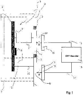
Fig. 1 shows, in a schematic representation, the structure of the device
according to the invention, according to a first embodiment of the
invention;
Fig. 2 shows, in a simple representation, a circuit on which the device
according to the invention could be based;
Fig. 3 shows, in a schematic representation, the structure of the device
according to the invention, according to a second embodiment of the
invention;
Fig. 4 shows, in a simple representation, a section of the production method
according to the invention; and
Fig. 5 shows, in a cross-section representation, the structure of a coin
containing the device according to the invention.
In Fig. 1, in a schematic representation, the device according to the
invention is shown
according to a first embodiment of the invention. An RFID transponder 1, which
preferably works in the UHF frequency range, has a substrate 2 and an RFID
chip 3.
The substrate portion of the RFID transponder 1 is arranged within a recess 5
of an
object 6 - 8, which can be a coin, for example.
A first surface unit 7, which also represents a cover of the remaining coin
body 6, is
opposite a second surface unit 8 of annular form. It should be noted that this
representation can be a cross-section through a circular coin, with insulating
elements
13, which can represent an electrically insulating ring, electrically
insulated.
A first connecting line 9 runs from the RFID transponder 1 to the first
surface element
7, and a second connecting line 10 runs from the RFID transponder 1 to the
second
surface element 8.
CA 02719184 2010-08-27
9A-112 113
8
The first connecting line 9 can have in its course a matching circuit 11,
which is used to
match the electrical terminal impedance of the chip 3 to the whole remaining
circuit to
be connected, as shown in more detail in Fig. 2. The matching circuit is
optimally
dimensioned with appropriate parameters for optimal power transmission and for
the
required frequency characteristic of the whole structure.
The first and second surface elements are electrically conductive surfaces
such as coins
usually have.
A third surface element 14 is separated from the first surface element 7 by a
first gap
20. A fourth surface element 15 is similarly separated from the second surface
element
8 by a second gap 19. The result of the surfaces, which are opposite each
other, of the
first and third surface elements, and of the second and fourth surface
elements, and
their preferably parallel alignment to each other, is arrangements like plate
capacitors,
which can be used to set up a capacitive coupling between the surface
elements, which
consist of electrically conductive material. The result of this is that by
means of the
capacitive coupling, a reader 18, which is connected to the third and fourth
surface
elements 14, 15, works in the UHF range, and is connected by the connecting
lines 16,
17, can carry out contactless communication, e.g. for data transmission, with
the chip 3
and thus the RFID transponder. The first connecting line 9 is connected to a
first
connection surface of the chip 3 or a further first connection surface, which
is
connected to these first connection surfaces, on the substrate, and the second
connecting line 10 is connected to a second connection surface of the chip 3
or a
further second connection surface, which is arranged on the substrate and
connected to
these second connection surfaces.
The first surface element 1 can be a cutout, e.g. in the form of a
mechanically broken-
out section, of the greater electrically conductive second surface element.
What is
decisive here is that the two surface elements or electrically conductive
layers are
insulated electrically from each other.
The surface elements 7, 8, 14 and 15 can, for example, be metal plates in
electrically
conductive form. The gaps 19, 20, and if appropriate the bases of the surface
elements
CA 02719184 2010-08-27
9A-112 113
9
in the form of capacitors, affect the effective coupling of the reader to the
RFID
transponder, and thus the stable functioning of transmission of data between
the RFID
transponder 1 and the reader 18.
The form of the coin body 16, shown with a dashed line, is intended to show
that the
device according to the invention is capable of functioning even without the
parts which
are shown with a dashed line, i.e. only with the surface units 7 and 8, the
result of
which is only one wall of electrically conductive material, said wall being
arranged
between the RFID transponder 1 and the reader 18 with the associated surface
elements 14, 15.
If according to the dashed line the second surface element 8 is parts of a
housing 6, a
capacitor 12 can be additionally arranged to form a circuit capacitor.
In Fig. 2, in a simple representation, a circuit of the device according to
the invention is
shown. Equal components and components with equal meaning are given equal
reference symbols.
From the representation, it can be seen that in a housing 6, which for example
can be a
coin body, the RFID transponder 1 is arranged with a chip, it being possible
to
represent the transponder as electronic components by means of a resistor 21
and a
capacitor 22.
Additionally, the matching circuit 11 is arranged in the coin body 6 for
inductive
matching. For a parasitic circuit capacitor, the capacitor 12 is connected
parallel to the
matching circuit and the RFID transponder 1.
The capacitive coupling which is built up between the first and third surface
elements 7,
14 is represented by a capacitor. Similarly, the capacitive coupling between
the second
and fourth surface elements 8, 15 is represented by a capacitor. Both
capacitors are
connected by the connecting lines 16, 17 to the UHF reader 18, which includes
a power
supply 24 and a resistor 25.
CA 02719184 2010-08-27
9A-112 113
In Fig. 3, the structure of the device according to the invention is shown
according to a
second embodiment of the invention. This representation shows that a housing
or a
coin body 6, which has the second surface element 8 as a part, can be
involved. Equal
components and components with equal meaning are given equal reference
symbols.
5
According to a second embodiment of the invention, such a completely closed
metal
housing 6 of electrically conductive material makes it possible to arrange the
fourth
surface element 15a with a gap 19a to the underside 6a or rear wall 6a of the
coin body
6, the result being an arrangement of the whole coin body 6, with the RFID
transponder
10 1 arranged in it, between the two surface elements 14, 15a of the reader
18.
Consequently, a reader with its plate elements 14, 15a acting like a capacitor
can easily
be placed on the top or underside of a coin.
Fig. 4 shows a section of a method according to the invention for the device
according
to the invention. Equal components and components with equal meaning are given
equal reference symbols.
On a substrate 2, contact surfaces 26 are arranged. First, a quantity of
adhesive 27 is
applied to the contact surfaces, so that next an RFID chip 3, with chip
connection
surfaces 28 under it, can be applied to the substrate 2, preferably by means
of a flip
process from a chip wafer. The chip is thereby joined by permanent adhesion to
the
connection surfaces 26, and thus to the inlet substrate 2, by means of the
previously
applied adhesive mass 27. The connection surfaces 26 can be separately
arranged
connection surfaces of the substrate 2.
The adhesive mass can be, for example, an anisotropic adhesive (ACA adhesive),
which
makes an electrical connection between the RFID chip connections and the
substrate
connections 26 possible.
Next, when pressure is applied, curing and bonding by the effect of
temperature for a
suitable time take place, and a connection between the chip connection
surfaces 28 and
the substrate connection surfaces 26 takes place. This is shown by the double
arrows
29.
CA 02719184 2010-08-27
9A-112 113
11
Alternatively, the connection between the substrate contact surfaces or
substrate
connection surfaces and the chip connection surfaces 28 can be made by means
of a
soldered joint or a self-conducting paste such as an isotropic paste.
The previously described matching circuit 11 can be integrated on the RFID
inlet
substrate 2 by implementing it as part of the substrate. This can be done, for
example,
by the matching circuit or further electronic components for desired
inductance and/or
capacitance effects being in the form of so-called strip transmission lines
via track
geometries.
The RFID chip, after being mounted on the inlet substrate 2, can be protected
from
environmental effects by being encapsulated in a suitable plastic material.
The RFID inlet substrate 2 can consist of a rigid or flexible line carrier
material.
As a further step in the production method according to the invention, the
inlet
connection surfaces 26 are connected electrically to the surface elements 7,
8. In this
case the electrical connections between the substrate connection surfaces 26
and the
electrically conductive layers or surface elements 7, 8 can be created by
means of
various connection processes. Depending on the properties of the materials to
be
contacted, of their surfaces and of the mechanical construction which is aimed
at,
electrical connection by soldering, welding, crimping, screwing or similar can
be chosen.
Similarly, suitable conductive pastes and adhesive masses can produce
mechanical
fixing and an electrically conductive connection. For this purpose, epoxy
adhesives and
silver conductive pastes are suitable, for example.
In a further step, a functional test of the RFID transponder (RFID inlet),
which is
arranged within the electrically conductive object, e.g. a coin, takes place.
For this
purpose, a UHF reader, which is coupled to the outer surfaces of the coins by
means of
the capacitive coupling with its third and fourth surface elements 14, 15, is
used, but a
gap between the surface elements 7, 14 and 8, 15 is retained. In this way the
function
CA 02719184 2010-08-27
9A-112 113
12
of the RFID transponder can be carried out without contact and without
restriction of
the specified RFID functions. It is important that the gaps 19, 19a and 20 are
maintained with a previously determined optimised order of magnitude.
In Fig. 5, the structure of a coin with the device according to the invention
is shown in a
cross-section representation. Equal components and components with equal
meaning
are given equal reference symbols.
Again, on a substrate 2 an RFID chip 3 and an antenna (not shown here in more
detail)
are arranged. A matching circuit 11 is also arranged on the substrate.
The RFID transponder is arranged with the substrate 2, the chip 3 and the
matching
circuit within a recess 5 of the coin body 6.
To fix the substrate within the recess 5, an epoxy adhesive mass 30 is
arranged on the
underside of the substrate, opposite a metallic base body 6a of the coin body
6.
Alternatively or additionally, further metal layers can be arranged between
the substrate
2 and the metallic base body 6a. A conductive adhesive mass 31 is arranged
circularly
on the metallic base body 6a on the underside in the round coin 6, so that in
this way
electrical contacting with the metallic base body 6a as a second electrically
conductive
surface element is obtained. For this purpose, a connection surface 32, which
is
preferably in annular form, and is arranged on the underside of the substrate
2, is also
used.
On its top side, the substrate has a further connection surface 33, which is
preferably
arranged annularly, and which is in electrical contact by means of
electrically conductive
adhesive elements 34, which are preferably in annular form, with sections 35
in annular
form of the first surface element 7, which acts as a capacitor surface, and
which also
represents the cover of the coin body.
The first surface element 7 is electrically insulated from the second surface
element 6a,
which also acts like a plate capacitor, by an insulating element 13,
preferably in annular
form.
CA 02719184 2010-08-27
9A-112 113
13
In the assembly, the RFID inlet substrate 2 is stuck to the second surface
element 6a,
and also within the coin body 6, by means of epoxy adhesive mass 31, and thus
mechanically fixed. Simultaneously, by means of a conductive adhesive, an
electrical
connection between the chip 3 and the surface element 6a of metallic material
is
produced. A combination of an epoxy adhesive and a conductive adhesive thus
exists,
and permits not only mechanical fixing, but also electrical contacting of the
RFID inlet to
the metallic base body. After the RFID inlet is installed in the metallic base
body 6, the
metallic body or the coin 6 is closed at the top by the surface element 7.
Both the fixing
of the surface element 7 and the connection to the matching circuit 11 are
again
achieved by means of epoxy adhesive and conductive adhesive masses 34.
Alternatively, other contacting methods such as contact springs, screwed
connections,
soldered connections and similar connections can be used for contacting the
RFID
transponder with the first and second surface elements 6a, 7 arranged on the
top and
underside.
The insulating element 13 is implemented by a plastic insert or by pouring,
e.g.
dispensing, the insulating mass into the filling space between the side walls
of the coin
body 6 and the cover 7.
All features which are disclosed in the application documents are claimed as
essential to
the invention if they are novel compared with the prior art, individually or
in
combination.
Reference symbol list
1 RFID transponder
3o 2 substrate
3 RFID chip
5 recess
6, 7 object
CA 02719184 2010-08-27
9A-112 113
14
6a, 8 second surface element
7, 14 surface element
9, 34 connecting element
10, 31 second connecting element
11 circuit
12, 22 capacitor
13 insulating element
14 surface element
15, 15a fourth surface element
8, 6; 15, 15a surface elements
16 coin body
16, 17 connecting lines
18 reader
19, 19a, 20 gap
21, 25 resistor
24 power supply
26, 28 chip connection surface
26 contact surface
27, 34 adhesive elements
29 double arrows
31 adhesive mass
32 second connection surface
33 first connection surface
35 sections