Note: Descriptions are shown in the official language in which they were submitted.
CA 02719306 2010-09-22
WO 2009/118457 PCT/F12009/050233
A COATING AND A METHOD FOR PRODUCING A COATING
BACKGROUND OF THE INVENTION
1. Field of the Invention
The present invention is related generally to surface protection coatings.
More
specifically, the present invention is related to plastic and metal components
that are
associated with a protective or hydrophobic coating.
2. Background Technology
Surface protective coatings on plastic or metal substrates produced by PECVD
(Plasma
Enhanced Chemical Vapor Deposition) have a wide potential application due to
their
hardness, abrasion resistance, adherence, attractive colour and other
properties.
Transparent surface protective coatings on transparent or metallic substrates
produced
by PECVD are prone to the appearance of so-called Newton rings or refraction
fringes
due to interference effects in in-door lighting conditions (One decorative
effect is the
iridescent visual effect created by multireflections). These interference
effects inhibit
the usage of the coating in a decorative function. The proposed surface
patterning of the
protective coating suppress the interference effects at the first surface,
suppress the
Newton rings and fringes and increase the optical transmittance of the
coating. The
application of these protective coatings abranges transparent plastic windows
for
handheld devices, all painting applications where the part is protected by a
transparent
top coat, all decorative and functional metal parts in devices where the
abrasion
resistance of the metal is not sufficient for the envisaged application,
vacuum metallized
plastic parts which need a topcoat for the protection of the metallic layer.
It is a well known technique to impart antireflective properties to an object,
such as a
sheet glass, by introducing microscopic corrugations to the surface of the
object [see for
instance: "Artificial Media Optical Properties-Subwavelength Scale", Lalanne
and
Hutley, published in the Encyclopedia of Optical Engineering, 2003]. We refer
to such
low reflectance surfaces as microstructured antireflective textures (MARTs).
The
microcorrugations of a MART typically are on a length scale sufficiently small
usually in the sub-wavelength regime to prevent diffusive scattering of light
CA 02719306 2010-09-22
WO 2009/118457 PCT/F12009/050233
commonly exhibited by a "matte" or "non-glare" finish. That is, a MART truly
reduces
the hemispherical reflectance from a surface rather than merely scattering or
diffusing
the reflected wavefront. In this regime, the interaction of light with a
microstructured
surface is usually described using an "effective medium theory", under which
the
optical properties of the microtextured surface are taken to be a spatial
average of the
material properties in the region [Raguin and Morris, "Antireflection
Structured
Surfaces for the Infrared Spectral Region", Applied Optics Vol. 32 No. 7,
1993]. The
hemispherical reflectance of light from glass back into air can be less than
0.5 % for a
properly designed MART. Such a small hemispherical reflectance is impossible
if the
surface corrugations are much larger than the wavelength of incident light.
For visible
light, the length scale of MART corrugations is typically around one-half
micron.
Perhaps the best known MART is the so-called "moth-eye" surface which
possesses
optical properties that may be more effective than commercially available thin-
film
coatings. Thin-film antireflective coatings usually consist of one or more
layers of
materials optically dissimilar from the substrate, and are sputtered or
evaporated onto
the substrate in precisely controlled thicknesses. Moth-eye surfaces are
comprised of a
regular array of microscopic protuberances, and are presently available from a
small
number of manufacturers worldwide (for example Autotype International Limited,
in
Oxon, England). Other examples of MARTs are the "SWS surface" [Philippe
Lalanne,
"Design, fabrication, and characterization of subwavelength periodic
structures for
semiconductor antireflection coating in the visible domain" pp. 300-309, in
SPIE
Proceedings Vol. 2776, (1996)], and the "MARAG" surface [Niggemann et al,
"Periodic microstructures for large area applications generated by holography"
pp 108,
Proceedings of the SPIE vol. 4438 (2001)].
Surface protective coatings, transparent or opaque, on transparent or metallic
substrates
produced by PECVD can be used to increase the hydrophobicity of the surface.
The
hydrophobicity of the surface depends on the chemical composition of the top
layer and
on the topography of the surface. The surface pattern created by the proposed
deposition
technology is capable to increase the water contact angle from between 95
...105 to
more than 150 which is a significant increase in hydrophobicity.
2
CA 02719306 2010-09-22
WO 2009/118457 PCT/F12009/050233
SUMMARY OF THE INVENTION
The formation of a thin film on a substrate by chemical reaction of gases is a
commonly
used industrial process. Such a deposition process is referred to as chemical
vapor
deposition or "CVD." Conventional thermal CVD processes supply reactive gases
to the
substrate surface where heat-induced chemical reactions take place to produce
a desired
film. Plasma enhanced CVD techniques, on the other hand, promote excitation
and/or
dissociation of the reactant gases by the application of radio frequency (RF)
or
microwave energy. The high reactivity of the released species reduces the
energy
required for a chemical reaction to take place, and thus lowers the required
temperature
for such PECVD processes. PECVD allows the deposition of hard protective
coatings
on plastic and metallic substrates. The proposed process influences the gas
flow onto
the substrate during the end of the deposition of the hard layer with an aim
to form a
patterned surface. The patterned layer may have a so-called moth-eye effect,
suppressing such multiple optical reflections. Another embodiment of the
proposed
process is a surface pattern which enhances the hydrophobicity of a surface to
a contact
angle with water greater than 1500.
These and other features of embodiments of the present invention will become
more
fully apparent from the following description and appended claims, or may be
learned
by the practice of the invention as set forth hereinafter.
According to an exemplary aspect of the invention, there is provided a
deposition
process or method for depositing a patterned coating, the method comprising:
depositing a patterned coating directly onto a curved or planar substrate
through a
patterning device by plasma enhanced chemical vapor deposition.
In an embodiment, the patterned coating comprises or consists of a plurality
of
protrusions. In an embodiment, the diameter of the protrusions is between 1 to
100 m,
the height of the protrusions between 0,01 to 0,5 m and the spacing between
the
protrusions 10 to 500 m. A small resolution patterning can thereby be
obtained. The
patterned coating may be uniform.
3
CA 02719306 2010-09-22
WO 2009/118457 PCT/F12009/050233
In an embodiment there is provided a method of producing a patterned coating
by
PECVD without additional production steps. An embodiment excels itself by the
provision that the proposed method produces a moth-eye like macrostructure on
a
surface by direct deposition. Additionally, the macrostructure may be
modulated by a
microstructure with a surface texture in the subwavelength range. As a result,
protective, antireflective coating comprising a carrier layer consisting of an
optically
transparent material, which, at least on one surface side, presents
antireflective
properties with respect the optical wavelengths of the radiation incident on
the surface
can be produced, as well as surface structures which are the basis for
superhydrophobic
surface properties.
BRIEF DESCRIPTION OF THE DRAWINGS
To further clarify the above and other advantages and features of the present
invention
and its embodiments, a more particular description of the invention will be
rendered by
reference to specific embodiments thereof that are illustrated in the appended
drawings.
It is to be appreciated that these drawings depict only typical embodiments of
the
invention and are therefore not to be considered limiting of its scope. The
invention will
be described and explained with additional specificity and detail through the
use of the
accompanying drawings in which:
FIG. la and FIG. lb represent a schematic depiction of typical production set-
ups
according to embodiments of the invention;
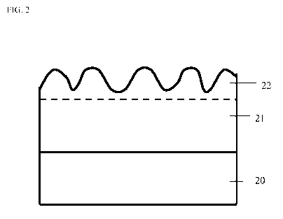
FIG. 2 shows a schematic depiction of a patterned coating;
FIG. 3a is a schematic depiction of an optical structure according to an
embodiment of
the present invention and FIG. 3b shows the optical reflection pattern of the
depicted
structure.
FIG. 4a is a schematic depiction of a structure according to another
embodiment of the
present invention, and FIG. 4b shows the optical reflection pattern of the
depicted
structure.
DETAILED DESCRIPTION OF THE INVENTION
One suitable PECVD (Plasma Enhanced Chemical Vapor Deposition) apparatus in
which the method of the present invention can be carried out is shown in FIGS.
la and
4
CA 02719306 2010-09-22
WO 2009/118457 PCT/F12009/050233
lb, which is a vertical, cross-sectional view of a PECVD system 4, having a
vacuum or
processing chamber.
PECVD system 4 contains a gas distribution manifold faceplate 2 for dispersing
process
gases 3 to a substrate 5 that rests on a pedestal 7, centered within the
process chamber.
Deposition and carrier gases are introduced into chamber 4 through perforated
holes of
a conventional flat, circular gas distribution 2. More specifically,
deposition process
gases flow into the chamber from the inlet manifold 1 through a conventional
perforated
blocker and then through holes in gas distribution faceplate 2.
Before reaching the manifold 1, deposition and carrier gases are input from
gas sources
12 through gas supply lines into a mixing system 13 where they are combined
and then
sent to manifold 1. Generally, the supply line for each process gas includes
(i) several
safety shut-off valves (not shown) that can be used to automatically or
manually shut-
off the flow of process gas into the chamber, and (ii) mass flow controllers
(also not
shown) that measure the flow of gas through the supply line. When toxic gases
are used
in the process, the several safety shut-off valves are positioned on each gas
supply line
in conventional configurations.
The deposition process performed in PECVD system 4 can be either a remote
plasma-
enhanced process or a cathodic plasma-enhanced process. In a remote plasma-
enhanced
process, an RF power supply applies electrical power between the insulated gas
distribution faceplate 2 and an auxiliar additional electrode or the chamber
wall. The
pedestal 7 is electrically connected to the chamber wall. In a cathodic plasma-
enhanced
process, an RF power supply applies electrical power between the insulated
pedestal 7
and an auxiliar additional electrode or the chamber wall. The gas distribution
face plate
is than electrically connected to the chamber wall. In both cases the RF power
excites
the process gas mixture to form plasma within the cylindrical region 9 between
the
faceplate 2 and the pedestal 7. (This region will be referred to herein as the
"reaction
region"). Constituents of the plasma react to deposit a desired film on the
surface of the
substrate supported on pedestal 7. RF power supply typically supplies power at
a high
RF frequency (RF) of 13.56 MHz or higher.
5
CA 02719306 2010-09-22
WO 2009/118457 PCT/F12009/050233
The substrates 5 are located on the pedestal 7, whereby flat substrates can be
located
directly onto the pedestal, a curved substrate is located on a holding device
with one
surface with the same curvature as the substrate in contact with the substrate
and with a
flat surface in contact with the pedestal 7.
In one preferred configuration depicted in FIG. la, a mesh or a perforated
plate 6 is
located between substrates and the reaction region (This mesh or perforated
plate will
be referred herein as "patterning device"). The patterning device 6 is
connected to the
pedestal 7. The distance between patterning device 6 and substrate surface can
vary
between 0,1 and 15 mm depending on the hole size and hole distance. In some
embodiments, the patterning device 6 is less than 2 mm thick. The patterning
device 6
may be made out of metal foil, textile web, glass, ceramics or plastic
material.
In an alternative configuration depicted in FIG. lb, the substrate 5 is
located directly on
top of the patterning device 6. The patterning device 6 is connected to the
pedestal 7. In
some embodiments, the patterning device 6 is be made out of electrical
conductive foil
or wires.
The remainder of the gas mixture, that is not deposited in a layer, including
reaction
byproducts, is evacuated from the chamber by a vacuum pump (not shown).
Specifically, the gases are exhausted through an annular orifice 8 through a
downward-
extending gas passage 10, past a vacuum shut-off valve 13, and into the
exhaust outlet
(not shown) that connects to the external vacuum pump (not shown) through a
foreline
(also not shown).
FIG. 2 depicts a typical structure on a transparent or opaque substrate 20,
which
includes a hard protective light transmissive layer 21 having a
macrostructured surface
relief pattern 22 the outer surface thereof.
Suitable materials for the substrate are almost all plastics used for
injection molding
including plastic materials such as polyvinyl chloride, polycarbonate, PC-ABS
polyacrylate and PET, metals like stainless steel and other steel alloys,
aluminium and
magnesium alloy.
6
CA 02719306 2010-09-22
WO 2009/118457 PCT/F12009/050233
The substrates may be pre-coated by different technologies, e.g., plastic
substrates could
be painted with a base coat to smoothen the surface and could be metallized
with a
metallic layer a thickness of 10 to 100 nm in a vacuum or electro-chemical
process. This
metal layer could consist in consisting in aluminium, indium, chromium,
silicon, iron,
nickel, tin or alloys of these materials.
Typical precursors and the resulting coating composition abrange transparent
coatings
type SiO,, based on pre-cursers like TMOS, HMDSO, HMDS, OCMTS etc, TiOX based
on pre-cursers like TiC14, Titanium tetraisopropoxide, (TiO)2 (tertiarybutyl-
acetoacetate)2, TiO[CH3000H_C(O-)CH3]2 and alloys of TiOX and SiOX and others.
Argon, helium and oxygen may be used as carrier gases and to enhance the
plasma
formed in region 9. Deposition conditions for the PECVD deposition process are
well
known by those skilled in the art. Layer 21 and 22 can be made based on the
same or
different precursors at similar deposition conditions.
During a typical production run, the PECVD reactor would be set (1) to deposit
the
hardcoating 21 as described above with the desired thickness without the use
of the
patterning device. In a subsequent step (2), the patterned layer 22 is applied
in the same
or similar reactor but by positioning the patterning device above or below the
substrate
into the reaction zone. If desired, a micropattern can be superimposed (3) on
the
macropattern obtained in (2) by repeating the patterning from step (2) but
with a
different patterning structure (hole size, hole form and hole distance) in the
patterning
device.
Embodiment 1
In one preferred embodiment, the substrate consists out of a flat or curved
transparent
plastic material like PMMA 30. HMDS is used as precursor, Oxygen and Helium as
carrier gases. Firstly a thick layer 2... 10 m of SiOX 31 is applied, while
removing the
patterning device. Secondly, an about 1...2 m thick SiOx layer 32 is applied
with the
patterning device, as depicted in FIG. 3a. The patterning device consists out
of a 0.2
mm thick metal foil with a regular pattern of holes with a diameter of 0,15
mm, spaced
about 0,3 mm. FIG. 3b depicts the optical transmittance pattern of the PMMA
substrate
33, with hard protective layer but without the patterned layer 34 and with
hard
7
CA 02719306 2010-09-22
WO 2009/118457 PCT/F12009/050233
protective layer and with the patterned layer 35 described in step 2. The
suppression of
the interference effect, its associated fringes and reduction of reflections
are apparent.
Embodiment 2
In another preferred embodiment depicted in FIG. 4a, the substrate 40 consists
out of a
flat or curved plastic material like PC-ABS. Firstly a 10... 15 m thick base
coat 41 is
applied by painting. In a second step a metal layer consisting of aluminium,
indium,
chromium, silicon, iron, nickel, tin or alloys of these materials 42 with a
thickness of 5
to 100 nm is applied in a vacuum process. Third, a thick layer 2...10 m of
SiOX 43 is
applied by while removing the patterning device. Forth an about 1...2 m thick
SiOX 44
layer is applied with the patterning device. The patterning device consists
out of a 0.2
mm thick metal foil with a regular pattern of holes with a diameter of 0,15
mm, spaced
about 0,3 mm.
FIG. 4b depicts the optical reflection pattern of a thin Indium film on a PC-
ABS
substrate 45, with hard protective layer but without the patterned layer 46
and with hard
protective layer and with the patterned layer 47 described in step 4. The
suppression of
the interference effect and its associated fringes is apparent.
Embodiment 3
In another preferred embodiment, the substrate consists out of a flat or
curved
transparent plastic material. Firstly a 10... 15 m thick base coat is applied
by painting.
In a second step a metal layer with a thickness of 10 to 100 nm is applied in
a vacuum
process. Third, a thick layer 2... 10 m of SiO,, is applied by while removing
the
patterning device. Forth an about 1...2 m thick SiO,, layer is applied with
the
patterning device. The patterning device consists out of a 0.2 mm thick metal
foil with a
regular pattern of holes with a diameter of 0,15 mm, spaced about 0,3 mm.
Fifth an
additional SiO,, layer is applied with a different patterning device. The
patterning device
consists out of a 0.2 mm thick textile mesh with a regular pattern of holes
with a wire
diameter of 0,065 mm and a mesh opening of 140 m. Sixth, the surface is
treated with
a commercially available product to form a thin (less than 10 nm) water
repellent layer.
8
CA 02719306 2010-09-22
WO 2009/118457 PCT/F12009/050233
As a result of the combined effect of the water repellent coating and the
surface
patterning, the surface turns itself super hydrophobic and a contact angle
with water of
superior 150 is achieved.
The present invention may be embodied in other specific forms without
departing from
its spirit or essential characteristics. The described embodiments are to be
considered in
all respects only as illustrative and not restrictive. The scope of the
invention is,
therefore, indicated by the appended claims rather than by the foregoing
description. All
changes which come within the meaning and range of equivalency of the claims
are to
be embraced within their scope. Having fully described several embodiments of
the
present invention, many other equivalent or alternative methods of depositing
the
protective PECVD layer according to the present invention will be apparent to
those
skilled in the art. These alternatives and equivalents are intended to be
included within
the scope of the present invention.
9