Note: Descriptions are shown in the official language in which they were submitted.
CA 02719753 2010-09-24
WO 2009/120695 PCT/US2009/038102
A POWER CONVERTER SYSTEM THAT OPERATES EFFICIENTLY OVER A RANGE
OF LOAD CONDITIONS
FIELD OF THE INVENTION
[00011 This invention relates to methods of designing and operating power
converters so
that their efficiency is optimized over the entire load range.
DESCRIPTION OF THE PRIOR ART
[00021 aver since the start of the miniaturization era spurred on by the
microelectronics
revolution in the late fifties and early sixties, power conversion equipment
employed in electronics
equipment and systems has been facing continuously increasing power density
and efficiency
challenges. Until recently, efficiency increases of power conversion circuits
were primarily driven
by increased power density requirements since power density increases are only
possible if
appropriate incremental improvements in full-load efficiency are achieved so
that the thermal
performance is not adversely affected. As a result, maximization of the full-
load efficiency has been
a design focus all along. However, in the early nineties, the explosive growth
of consumer
electronics and data-processing equipment had prompted the introduction of
various, mostly
voluntary, requirements aimed at minimizing the idle-mode, i.e., light-load,
power consumption.
Most notable light-load efficiency requirements are defined in 11,:x, Energy
Star and ECoC
(European Code of Conduct) specifications.
[00031 Today, the power supply industry is at the beginning of another major
focus shift
that puts efficiency improvements across the entire load range in the
forefront of customers'
performance requirements. This focus on efficiency has been prompted by
economic reasons and
CA 02719753 2010-09-24
WO 2009/120695 PCT/US2009/038102
and a relatively low energy efficiency of its power converter system. In fact,
the environmental
concerns have prompted Environmental Protection Agency (EPA) to revise its
Energy Star
specifications for power supply efficiencies by defining the minimum
efficiencies from full load
down to 20% of full load. However, major computer, telecom, and network-
equipment
manufactures already require light-load efficiencies that exceed the latest
Energy Star specifications
and also are extending these requirements down to 10% and, even 5% loads.
[0004] Generally, the efficiency of power conversion circuits at heavy loads
is determined
by conduction losses of semiconductor and magnetic components, whereas their
light-load
efficiency is primarily determined. by switching losses of semiconductors,
core losses of magnetic
material, and drive losses of semiconductor switches, as disclosed by M. D,
Mulligan, B. Broach,
T.H. Lee, "A constant-frequency method for improving light-load efficiency in
synchronous buck
converters", IEEE Power Electronics Letters, Volume 3, Issue 1, March 2005,
pp. 24 - 29. Because
switching and drive losses of semiconductor switches and core losses of
magnetic components are
almost independent of the load current, a typical efficiency curve as a
function of the load current
shows a steep fall off as the load current decreases beyond 20-30% of the full
load current. In facto
in a typical power converter, the light load eff"iciency, e.g., efficiency at
10%, is significantly lower
than that at full load. This difference increases as the rated output current
(power) of converter
increases because higher power requires the use of larger semiconductor
devices (or more devices in
parallel) and larger magnetic cores which inherently exhibit increased
switching and core losses,
respectively.
[0005] Generally, the minimization of the conduction losses, i.e., the full-
load efficiency
~_on ~.cto S ec ica the .. ~. at f .. :., .., ...
CA 02719753 2010-09-24
WO 2009/120695 PCT/US2009/038102
of MOSFETs with minimum on-resistances and rectifiers with minimum forward
voltage drops,
whereas the conduction loss of magnetic components such as input- and output-
filter inductors,
transformers, and interconnect losses are minimized by reducing the resistance
of copper
conductors, i.e., by shortening the length and increasing the cross-section of
wires and PCB traces.
The minimization of core losses ofinagnetic components, switching losses of
semiconductors, and
drive losses is based on the selection of optimal switching frequency and the
use of low-loss
magnetic materials, MOSFET switches with inherently lower switching losses,
and rectifiers with a
low reverse-recovered charge and/or by employing various soil-switching
techniques that
substantially reduce switching losses of semiconductors, as disclosed by X.
wang, F. Tian, Y. Li, I.
Batarseh, "High Efficiency high Power Density DC/DC Converter with Wide Input
Range", in
, pp. 2115-2120, Oct. 2006.
Proc. lASAnnual Afeeling
[0006] However, very often, the described efficiency optimization techniques
may not be
enough to make the power supply exhibit the efficiency curve that meets
customer's expectations.
This is especially true for ac/dc (off-line) power supplies intended for high-
power applications. In
this case, it is a common practice to resort to power-supply-level power
management techniques to
further improve partial-load efficiencies. Generally, these techniques are
based on changing
operation mode based on the load current and/or input voltage conditions. The
most used power
management techniques practiced today are variable switching frequency
control, hulk-voltage
reduction technique, phase-shedding tech niglue, and "burst"-mode operation
technique. While all
these load-activity-based power management techniques have been implemented
using analog
technology, the current rapid employment of digital technology in power
conversion applications
has made their implementation much easier.
CA 02719753 2010-09-24
WO 2009/120695 PCT/US2009/038102
[0007] In the variable-switching-frequency approach, the switching frequency
of a
converter is reduced as the load current reduces, as disclosed by Jingdong
Chen, "Determine Buck
Converter Efficiency in PFIVI Mode", Power Electronics Technology, September
2007, pp. 28 - 33.
Because the switching loses is proportional with the switching frequency this
method improves the
light load efficiency. In its simplest implementation, the switching frequency
is not continuously
reduced as the load gets lighter, but it is only switched to a lower fixed
frequency when the load
current falls below the preset threshold level.
[0008] In off-line converters that require active power-factor-correction
(PFC) front-end,
reduction of energy-storage (bulk) voltage has been extensively used to
improve the light load
efficiency, as disclosed by P. Vinciarelli in US Patent No. 5,289,361. This
method is based on the
fact that the switching losses in semiconductor components such as MOSFET
switches and fast-
recovery diode rectifiers are reduced if the voltage that they need to switch
off is reduced. In a
typical universal-line (90-264 Vrms) ac/dc power supply with a PFC front end,
the bulk voltage is set
slightly above the peak of the maximum line voltage, i.e., at around 400 V,
and the bulk capacitor
value is determined so that the bulk cap can support the full power for a
specified hold-up time,
which is usually in. the 12-ass to 20-ms range. Since at a partial load the
bulk-cap energy required to
support the output during the hold-up time can be stored at a lower voltage,
the bulk cap voltage can
be reduced as the load decreases to improve the light-load efficiency, The
range of the bulk voltage
is limited by the regulation-range of the downstream dc/ dc: output stage.
[0009] In power converters that are implemented with multiple stages, the
stage-shedding
technique is often employed to increase the light load efficiency, as
disclosed by S. W. f lobrecht
i:....\: .\. \.. '..... S y- ~ :. ;zlhis h` nol~ \ for
w .tea. -ss ht 'o'-ad, "'re .. . l off so, ha.. . boss is e'inainaited. . ` in
4
CA 02719753 2010-09-24
WO 2009/120695 PCT/US2009/038102
power supplies with front-end Pl-,, the PFC stage can be turned off when the
input power hills
below 75 W, which is the lower input-power limit that requires PFC. Also, in
desktop power
supplies, the amain power convertor channel, i.e., both the PFC front end and
the downstream
multiple output dc/dc converter, are turned off in the standby mode and the
standby power is
supplied by a. low-power standby converter. By completely eliminating the
losses of a large high-
power .PF C and do/dc converters, the standby power consumption can be
substantially reduced,
typically, below > W. Finally, the stage-shedding technique is extensively
used to improve light
load efficiency of power converters that utilize paralleled or interleaved
stages such, for example,
Voltage regulation modules (VRMs), When applied to interleaved power
processing stages, this
technique is commonly referred to as the phase-shedding technique.
[00101 Finally, J. Choi, D. Huh, Y. Kim, "The improved burst mode in the stand-
byr
operation of power supply", IEEE App ied Power Electronics (APEC) Coy- f
Proc., pp. 426-432,
2004, disclose a converter that in "burst"-r-node is turned-off for r post.
ofthe' rri.e and the load is
supplied by the energy stored in the output filter capacitor. To replenish
this energy, the converter is
turned-on periodically for a brief period of time. Since the converter stays
off for the most of the
tithe, its loss is substantially reduced, which increase the efficiency. The
"burst"-mode of operation
is supported by the majority of commercially available I:C controllers,
100111 Although the described techniques have been shown to improve the
partial-load
efficiency, they suffer from some major drawbacks that limit their area. of
application. For examp e,
the major problem o reducing the switching frequency at light loads is an
increased current ripple
caused by increased. volt-second product in the core of the output filter
inductor. Th s increase in the
. _, c a. s it the. c .....,.;..,. s.
CA 02719753 2010-09-24
WO 2009/120695 PCT/US2009/038102
major concern with the hulk-voltage reduction and stage-shedding techniques is
the dynamic
performance. Specifically, their ability to restore full-power capability
without output disturbance or
other performance deterioration when the load suddenly changes from light load
to full load.
Finally, the "burst"-mode operation is limited to very low power levels
primarily due to acoustic
noise.
[0012] In this invention, implementations of power converters that offer
maximized light-
load efficiencies without the limitations of prior-art techniques are
described.
SUMMARY OF THE INVENTION
[0013] Briefly according to one aspect of the present invention, a power
converter system
supplies power to one or more loads. The power converter system comprises at
least one power
converter operating at a desired efficiency; and a power storage system
coupled to the at least one
power converter for receiving power supplied from the at least one power
converter and storing
power therein when the at least one power converter operates at an efficiency
that is below the
desired efficiency.
[0014] According to another aspect of the present invention, a power converter
system
supplies power to at least one load., The power converter system comprises at
least one power
converter that supplies uninterrupted power to the at least one load anytime
the power converter is
operating at a desired efficiency; and a power storage system coupled to the
at least one power
converter for receiving power supplied from the at least one power converter
and storing power
therein when the at least one power converter operates at an efficiency that
is below the desired
efficiency.
[O0151 According to still another aspect of the present invention, a power
converter system
,a
111 11's lno,,-n 6
CA 02719753 2010-09-24
WO 2009/120695 PCT/US2009/038102
condition. The power converter system comprises at least one power converter
supplying
uninterrupted power at the higher load condition at a desired efficiency; and
a power storage system
coupled to the at least one power converter for receiving power supplied from
the at least one power
converter and storing power therein under the lower load condition.
[00161 According to some of the more detailed features of the present
invention, a power
converter system supplies power to one or more loads. The power converter
system comprises one
or more power converters. Each power converter operates at a desired.
efficiency under a load
condition. Any time the efficiency of a power converter drops below the
desired efficiency or an
efficiency threshold, the power converter is sequentially turned on during a
first time interval and
turned off during a second time interval. During the first time interval, the
power converter operates
at the desired efficiency to supply power to a power storage system. During
the second time
interval when the power converter is turned off, the power storage system
operates auxiliary to the
power converter to supply power to a load.
[0017] According to some of the more detailed features of the present
invention, a power
converter system powers one or more loads. The power converter system includes
at least one
power converter that supplies uninterrupted power to the load anytime the
power converter is
operating at a desired efficiency. The supply of power from the at least one
power converter to the
load is partially interrupted any time the power converter operates at a lower
efficiency than the
desired efficiency such that. the at least one power converter is turned on
during a first time interval
and turned off during a second time interval. A power storage systern operates
auxiliary to the at
least one power converter. During the first time interval, the at least one
power converter operates
at the desired efficiency to supply power to the power storage system. During
the second time
CA 02719753 2010-09-24
WO 2009/120695 PCT/US2009/038102
interval when the at least one power converter is turned off, the power
storage system supplies
power to the one or more loads.
[0018] According to some of the more detailed features of the present
invention, a power
converter system supplies power under load conditions that range from a higher
load condition to a
lower load condition. One or more power converters supply uninterrupted power
at the higher load
condition at a desired efficiency and supply partially interrupted power at
the lower load condition.
The power of the power converter is partially interrupted by turning it on
during a first time interval
and turning it off during a second time interval. A power storage system
operates auxiliary to the
power converter. The power converter operates during the first time interval
at the desired
efficiency for supplying power to the power storage system and for supplying
power under the
lower load condition. The power storage system supplies power under the lower
load condition
during the second time interval when the power converter is turned off.
[0019] According to some of the more detailed features of the present
invention, the power
converter has a first output for supplying power to the power storage system
during the first time
interval and a second output for supplying power to the at least one load
during the second time
interval. Alternatively, the power converter has a single output for supplying
power to the power
storage system during the first time interval and supplying power to the at
least one load during the
second time interval. In another exemplary embodiment, the power storage
system has a single port
for receiving supply of power from the power converter during the first time
interval and supplying
storage system has a first port for receiving supply of power from the at
least one power converter
`_ one
CA 02719753 2010-09-24
WO 2009/120695 PCT/US2009/038102
the second time interval. The power converter, the power storage system and
the load are coupled in
series,
[0020] According to other more detailed features of the present invention, the
power
converter comprises a power stage and an output filter, In one embodiment, the
power storage
system supplies power to the load via the output filter. In another
embodiment, the power converter
supplies power to the power storage system via the output filter. In various
exemplary embodiments
of the invention, the power converter comprises at least one of isolated, non-
isolated, single-stage
and multi-stage, ac:/dc, dc./dc, do/ac, and ac/ac power converter.
[0021] According to other more detailed features of the present invention, the
power
converter system further comprises a controller coupled to the at least one
power converter and the
power storage system for controlling the operations of the at least one power
converter and the
power storage system.
BRIEF DESCRIPTION OF THE DRAWINGS
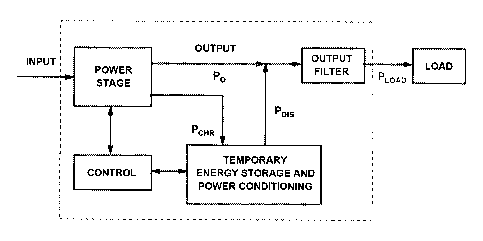
[0022] Figure 1 shows a block diagram of preferred embodiment of the present
invention.
[0023] Figure 2 shows the power flow timing diagram of the preferred
embodiment in Fig.
1 at higher load conditions. Po is output power, PCHR is charging power, and
PDis is discharging
power.
[0024] Ãgure 3 shows the power flow timing diagram of the preferred embodiment
in Fig,
I at lower load conditions. Po is output power, PCH;t, is charging power, and
PD,s is discharging
power.
[0024] Figure 4 shows typical efficiency profile of power converter with
respect to
CA 02719753 2010-09-24
WO 2009/120695 PCT/US2009/038102
[0026] Figure 5 shows the embodiment of the present invention with charging
energy of
the independent power storage system directly supplied from the output of the
power converter.
[0027] Figure 6 shows the embodiment of the present invention with a common
charging
and discharging power paths coupled to output of the power converter.
[0028] Figures 7(a)-7(d) show embodiments of the present invention with the
independent
power storage system connected at the input of the output filter of the power
converter.
[0029] Figure 8 shows an embodiment of the present invention with the
independent
power storage system in series with the power converter.
[0030] Figure 9 shows an embodiment of the present invention with the
independent
power storage system connected at the input of the output filter of the power
converter in, multiple
power converters connected in parallel at the output.
[0031] Figure 10 shows the embodiment of the present invention with the
independent
power storage system connected at the input of the output filter of the power
converter in multiple
converters with independent outputs.
[0032] Figures 11(a)-(h) show various implementations of temporary energy
storage and
power conditioning circuit for embodiments with the independent power storage
system connected
at the input or the output of the output filter of a do/dc power converter.
[0033] Figures 12(a)-() show implementations of atwo-switch forward do/plc
converter
for embodiments with the independent power storage system connected at the
input of the output
filter.
[00341 Figures 13(a)-(h) show imp lenmeritations of a full-bridge dc/dc
converter for=
embodiments with the independent power storage system connected at the input
of the output filter.
t-~
CA 02719753 2010-09-24
WO 2009/120695 PCT/US2009/038102
[0035] Figure 14 shows implementations of a hall-bridge dc/ dc converter for
embodiments
with the independent power storage system,
[0036] Figures 15(a)-(c) show implementations of a LLC resonant do/dc
converter for
embodiments with the independent power storage system connected at the input
of the output filter.
[0037] Figure 16 shows implementations of a half-bridge LLC resonant dc/dc
converter.
[0038] Figures 17 (a)-(b) show implementations of a forward dc/dc converter
for
embodiments with the independent power storage system connected at the input
of the output filter.
[0039] Figure 18 shows implementations of a flyback dc/dc converter with
separate
charging and discharging paths.
[0040] Figures 19(a) and (b) show implementations of a three-stage ac/dc
converter for the
embodiment of the present invention with the independent power storage system
in series with the
power converter.
DETAILED DESCRIPTION OF THE INVENTION
[0041] A power converter system supplies power to one or more loads. The power
converter system comprises one or more power converters. Each power converter
operates at a
desired efficiency under a load condition. The power converter systern.
further comprises a power
storage system coupled to the one or more power converters for receiving power
supplied from the
one or more power converters and storing power therein. When the efficiency of
the power
converter is below the desired efficiency, the power converter operates at the
desired efficiency to
supply power to the power storage system. Namely, the power converter system
supplies power
under load conditions ranging from a higher load condition to a lower load
condition. The power
ping uninterrupted power at the
1 ,
, = tie ...
t
a
CA 02719753 2010-09-24
WO 2009/120695 PCT/US2009/038102
power storage system coupled to the one or more power converters for receiving
power supplied
from the one or more power converters and storing power therein under the
lower load condition,
[0042] According to one aspect of the present invention, a power converter
system
supplies power to one or more loads, The power converter system comprises one
or more power
converters. Each power converter operates at a desired efficiency under a load
condition. Any time
the efficiency of a power converter drops below the desired efficiency or an
efficiency threshold,
the power converter is sequentially turned on during a first time interval and
turned off during a
second time interval. During the first time interval, the power converter
operates at the desired
efficiency to supply power to a power storage system, Preferably, the power
converter operates at
the desired efficiency to supply power to an independent power storage system.
During the second
time interval when the power converter is turned off, the independent power
storage system. operates
auxiliary to the power converter to supply power to a load. The power
converter system further
comprises a controller coupled to the at least one power converter and the
power storage system fhr
controlling the operations of the at least one power converter and the power
storage system,
[0043] The power system of the present invention maintains high efficiency for
one or
more power converters across the entire load range, including higher load
conditions (e.g., full
loads) and lower load conditions (e.g., light loads). Specifically, the system
of the invention
substantially increase the conversion efficiency at light loads by minimizing
switching and drive
losses of semiconductor switches and core losses of magnetic components. These
losses at light
loads are minimized by sequentially turning on the power converter during a
first time interval and
turning off the power converter during a second time interval. In this way,
the power converter
partially interrupts the supply of power from the input to the output for a
period. of time. While the
1 .\
CA 02719753 2010-09-24
WO 2009/120695 PCT/US2009/038102
independent power storage system, such as a low-power supplementary converter.
In one
exemplary embodiment, the independent power storage system operates as
auxiliary to the power
converter for supplying power to the load, when the power converter is turned
off. The independent
power storage system is supplied from an energy source that is charged during
the periods the
power converter is operating at a desired optimum efficiency, when
transferring power from the
input to the output. Since the independent power storage system is not
supplied from the input of
the main power converter, but from the power converter that generates an
auxiliary energy source,
the independent power storage system can be a simple non-isolated converter
even in applications
that require isolation. In fact, by creating the auxiliary energy source on
the secondary side of the
transformer in an isolated converter, the independent power storage system
performance is
optimized
[00441 Unlike conventional power systems, the system of the present invention
does not
exhibit any transient problems when the load is abruptly changed from light to
full load and the
normal operation with continuous delivery of power at the descried optimum
efficiency from the
input to the output is resumed because the independent power storage system is
arrange sÃs that. it
shares the low-pass output filter with the main power converter. As a result,
the energy in the
energy-storage components of the output filter, i.e., inductors and/or
capacitors, is always the same
immediately before and after a load transition making the transient behavior
to be identical to that of
the main converter.
100451 Generally, the ratio of the time duration during which the power
converter
processes the input power and the time duration it is decoupled from the input
is dependent on the
load power and the level of power that the main converter is processing when
it is coupled to the
lvu,
CA 02719753 2010-09-24
WO 2009/120695 PCT/US2009/038102
power converter. The frequency of the first time interval when the main power
is turned on and the
second time interval when the main power converter is turned off can be
arbitrarily selected
provided that it is lower than the crossover frequency of the power converter.
To maximize the
light-load efficiency, the power processing when the main power converter
supplies power to the
loads should be done at the level that exhibits the desired optimurn
efficiency.
[0046] Alternatively, any time the at least one power converter operates at an
efficiency
that is below the desired efficiency, the power converter operates at the
desired efficiency to supply
power to the power storage systern and the power storage system supplies power
to the at least one
load simultaneously. Alternatively, any time the at least one power converter
operates at an
efficiency that is below the desired efficiency, the power converter operates
at the desired efficiency
to supply power to the power storage system and the at least one load and the
power storage system
supplies power to the at least one load simultaneously.
[0047] The present invention is applicable to any power conversion circuit.
Specifically, it
is applicable to isolated and non-isolated, single-stage and multi-stage, ac/
dc, dc/dc, dc/ac, and ac/ac
power supplies. The present invention is applicable to any power converter
system. Specifically, it
is applicable to power conversion system for LE=lD, power conversion system
for solar cell, power
conversion system for fuel cell, power conversion system for wind energy,
power conversion
system for vibrating energy, power conversion system for kinetic energy, power
conversion system
for thermal energy, power plant, power management and conversion system for
architecture, power
management and conversion system for data center, UPS, power conversion system
for vehicle,
power conversion system for computer or notebook, power conversion system for
communication
device or apparatus, power conversion system for consumer electronics product,
power conversion
CA 02719753 2010-09-24
WO 2009/120695 PCT/US2009/038102
[00481 The present invention is better understood upon consideration of tile
detailed
description below and the accompanying drawings.
[00491 A block. diagram of the preferred embodiment of the present invention
that
maximizes the lower load condition or light-load efficiency of a power
converter is shown in Figure
1. The power system shown in Figure 1 supplies power to a load. In one
exemplary embodiment,
the power system comprises a power converter, an independent power storage
system, and control
circuit. Generally, the power converter in Figure 1 can be any single-stage or
multi-stage, isolated
or non-isolated ac/dc, dc/dc, dc/ac, or ac/ac converter. The independent power
storage system can
comprise any energy storage device, medium, or component capable of storing
energy such, for
example, one or more capacitors, super capacitors, batteries, flywheels, fuel
cell, etc.
[00501 The independent. power storage system in Figure 1 only operates to
supply power
under lower load or light load conditions, preferably, below a certain level
of load power. Above
this power level up to the full load, the independent power storage system is
turned off so that the
entire load power is continuously supplied from the output of the power
converter in an
uninterrupted manner, as illustrated by the power flow diagram in Figure '2.
As can be seen from
Figure 2, at heavy loads, the both charging power PCHR and discharging power
PDIS are continuously
zero, whereas output power of the power converter Po is equal to load power
PLOAD.
[005.11 At light loads, ho~;wever, the power converter is sequentially or
periodically turned
on during a first time interval and turned off during a second time interval
to reduce switching
losses and, thus, improve the light-load efficiency. During the second fine
interval when the power
converter is off the load power is supplied from the independent power storage
system through a
temporary energy storage and power conditioning circuit. As can. be seen from
the power flow
CA 02719753 2010-09-24
WO 2009/120695 PCT/US2009/038102
converter is operated at the desired efficiency to simultaneously supply load
power PLOAD and
charge power of the independent power storage system. During the second time
interval when
the power converter is turned off, the load power is entirely supported by the
discharging of the
independent power storage systems. Since in. this mode of operation the load
power is either
supplied by the power converter output or by the stored energy, the
instantaneous power delivered
by the power converter during the first time interval called the on time TON
is PO===PLOAD and the
instantaneous power delivered from the independent power storage system during
the second time
interval called off time '0rF is PD{s=PLOAD~ Defining duty cycle D as
D=TON/(TON-'TOrr), average
power delivered by the converter output is PO(AV)=DPLOAD, whereas the average
power discharged
from the independent power storage system is PDrs(AV)===:(l D)PLOAD= Since
average charging power
PCHR(AV) must be equal to average discharging power PDIS(AV), the average
charging power is
PCHR(AV)=(l-D)PLOAD. As a result, the instantaneous charging power PCHR during
on time TON is
PCHR=(1-D)PLOAD/D, as illustrated in Fig.:. Therefore, total instantaneous
power P delivered by the
power converter during on time is
1 _. D 3LOA1J-
P = PO ' " Pclm = pL.OAO -1- ----I~ ---- PLOAD D , (1)
i.e.,
I LOAD = 1) > I (2)
[0052] Thus the power converter of the present invention operates in a
continuous modes
When
the efficiency drops below an efficiency threshold, the power converter
operates in a pulsed mode
when it is sequentially turned on and off as described above. It should be
noted that boundary load
modes ,pe ` ~, ve
16
CA 02719753 2010-09-24
WO 2009/120695 PCT/US2009/038102
at a suitable efficiency threshold level, which could be any arbitrary level.
However, to optimize the
performance, the control of the power converter cban be designed so that the
instantaneous power P
delivered by the power converter during the first time interval, i.e., on
time, is selected at a desired
efficiency, which can be the maximum efficiency point, As illustrated in Fig.
4, a typical power
converter efficiency dependence on output power exhibits a peak at mid-range
power levels. By
selecting P=POPT, i.e., by always operating the converter at the power level
with maximum
efficiency 1M X, the light-load efficiency below the set level of PBoUND (Popp-
r;.) is maximized. With
such a control, duty cycle D is determined by
U91J D sD
D ) P 1,014D BOUMT) . .d OF7
OP"
[00531 By assuming that the energy-storage device charging and discharging
efficiencies
are 'ncHR and f Dis, respectively, the conversion efficiency at power levels
below PBOUND is given by
27 __ 'lM4t' __ 17,s.114X (4)
1 D 1-D
D
D 77CHR ' T/DIS 7h, S
where 'f r s=: q .I-IR DIS is the efficiency of the total power process by
energy storage and power
conditioning block.
[0050 In the ideal case when no energy is lost during the charging and
discharging of the
energy-storage device, i,e., when rs= l is assumed. light-load efficiency it
is equal to t]I,IAx all the
way to a minimum load, as illustrated in Figure 4. However, in practice,
because 'r;~s<l the light-
load efficiency is lower than II,.MAX and exhibits a fall-off as power is
reduced, as shown in Figure
CA 02719753 2010-09-24
WO 2009/120695 PCT/US2009/038102
trade-off between the power saved by periodically turning-off the power
converter and the pow %e.r
lost in the charging and discharging process of the energy-storage device. By
solving Eq. (4) for
liES, minimum efficiency IJES(MIN) required to improve efficiency at load
power PLL is
T( -
/ES(MIN) > (1 D) '
17OPT_ - D
17LL
where TiLL is the original efficiency of the power converter at PLL and D:
=:PLt/POPT.
[00551 It should be noted that while duty cycle D is precisely defined by Eq.
(3), once
power level POPT is set and load power P;_OAr)<PBOUND is kno-~wwn, the
frequency at which the power
converter is turned on and off is less well defined. Generally, the upper
frequency limit is related to
the large signal dynamic response time of the converter, whereas the lower
frequency limit is
determined by the size and required energy-storage capacity of the energy-
storage device because
more stored energy is required at lower frequencies to support the load power
during prolonged off
time. For power levels of several hundred Watts, typical minimum frequency for
electrolytic-
capacitor-type energy storage is in the several Hertz to several hundred of
Hertz range, whereas sub-
hertz frequencies can be achieved by employing batteries, flywheels, and
similar storage devices.
Finally, it should be noted that it is desirable to keep the switching
frequency bellow the audio range
to avoid acoustic noise associated with the switching of a relatively large
power,
[00561 Many variations of the embodiment of the present invention are
possible.
Generally, these variations are in the manner the charging and discharging
power paths of the circuit
are coupled to the power converter, Output, and load. Sortie examples of these
variations are given in
Figs. 5 through 8.
CA 02719753 2010-09-24
WO 2009/120695 PCT/US2009/038102
[00571 Figure 5 shows the embodiment of the present invention where the
charging energy
is supplied from by the output of the power converter to the independent power
storage system and
discharge energy form the independent power storage system is also supplied to
the load via the
output of the power converter, Figure 6 shows the embodiment of the present
invention with
charging energy PCHR supplied from the output of the converter that also
supplies the load power.
Under this arrangement, the power converter has a single output for supplying
power to the
independent power storage system during the first tine:: interval and
supplying power to the at least
one load during the second time interval in a bidirectional time multiplexed
manner. Thus, the
present invention can be implemented with common energy charging and
discharging paths.
[0058] Figures 7(a}-7(d) shows various embodiments of the present invention
where the
power converter comprises two stages: a power stage and an output filter
stage. Figure 7(a) shows
separate charging and discharging paths with charging power supplied from a
second output of the
power stage and discharging path to the load is supplied from the independent
power storage system
via the output filter. Figure 7(b) shows separate charging path supplied from
the output of the
power stage and discharging path from the independent power storage system is
also via the output
of the power stage into the load via the output filter. Figure 7(c) shows
common charging and
discharging paths between the power stage and the output filter. Figure 7(d)
shows separate
charging and discharging paths with charging power supplied from the output of
the output filter
and discharging path connected to the input of the output filter. The
implementations with common
charging and discharging paths require the employment of a bidirectional
converter in the
independent power storage system.
[0059] Generally, charging and discharging paths does not need to be coupled
directly to
e ., p.
CA 02719753 2010-09-24
WO 2009/120695 PCT/US2009/038102
stated above, Figures 7(a)-(d) shows various embodiments of the present
invention where the power
converter and the independent power storage systems share the output filter,
i.e., where the charging
and/or discharging paths are coupled before the output filter of the power
converter. If properly
designed, these implementations can reduce, or even completely eliminate,
transients caused by
periodic turning on and off of the power converter. Namely, since in these
implementations the
output-filter inductor current is continuously flowing, i.e., it is either
supplied from the converter or
from the discharging energy-storage device, it does not exhibit significant
transient if the circuit is
designed so that the current supplied by the converter when it is on and the
current supplied by
energy-storage device during off-time are reasonably matched.
[00601 In some applications coupling the independent power storage system in
series with
the power converter, as shown in Figure 8, may be more beneficial for
improving light-load
efficiency than the previous implementations with the independent power
storage system coupled in
parallel to the power converter. It should be noted that the present invention
can also be applied in
applications with multiple converter, as illustrated in Figures 9 and 10.
Figure 9 shows an
embodiment of the present invention with a shared output filter in multiple
power converters
connected in parallel at multiple outputs, whereas Figure 10 shows an
embodiment of the present
invention with independent multiple outputs.
100611 Figures I I (a)-(h) show various embodiment of the present invention
with a shared
output filter in multiple converters with independent outputs. More
specifically Figures 11 (a)-(h)
show various implementations of temporary energy storage and power
conditioning circuit for
embodiments with the independent power storage system connected at the input
of the output filter
of a dc/dc power converter, i 1 (a) shows common charging and discharging path
employing
v A `t i nve one =p . x the
.i ' ':-1i ost
,;i v'
CA 02719753 2010-09-24
WO 2009/120695 PCT/US2009/038102
converter comprises boost switch SL1, buck switch SL2, inductor L1., and
capacitor CL. Figure 11(b)
showing separate charging and discharging paths with charging power supplied
from the output of
the power stage and employing a boost converter for charging and a buck
converter for discharging.
In one exemplary embodiment, the boost converter comprises boost switch SLI,
boost diode DL!,
inductor L1.1, and capacitor CL. The buck converter comprises buck switch SL2,
buck diode DL2,
inductor LL2, and inductor LF. Figure 11 (c) shows separate charging and
discharging paths with
charging power supplied from the output of the power stage and employing a
boost converter for
charging and a buck converter for discharging, where the buck converter and
the power converter
share the output filter. In one exemplary embodiment, the boost converter
comprises boost switch
S-,,, boost diode DL, inductor F1., and capacitor C1;. The buck converter
comprises buck switch SL2,
the power-stage diode, inductor LF, and capacitor CF. I{ igure 11(d) shows
separate charging and
discharging paths with charging power supplied directly from a second output
of the power stage
and employing a buck converter for discharging. In one exemplary embodiment,
the buck converter
comprises buck switch SL, buck diode DL, inductor LL2, and inductor LF. Figure
11(e) shows
separate charging and discharging paths with charging power supplied directly
from a second output
of the power stage and employing a buck converter for discharging, where the
buck converter and
the power converter share the output filter. In one exemplary embodiment, the
buck converter
comprises buck switch SL, the power-stage diode, inductor L. F, and capacitor
C-. Figure 11(f) shows
separate charging and discharging paths with charging power supplied from a
second output of the
pi'_"vvcr e t Trough a boost charging circuit and employing a buck converter
for discharging. In
one exemplary embodiment, the boost charging circuit comprises boost switch
SL,, boost diode Dl,1,
...1to and a,..'. , The converter buck switch [luck diode D, .
-~ i
CA 02719753 2010-09-24
WO 2009/120695 PCT/US2009/038102
charging power supplied from a second output of the power stage through a
boost charging circuit
and employing a buck converter for discharging, where the buck converter and
the power converter
share the output filter, In one exemplary embodiment, the boost charging
circuit comprises boost
switch SL1, boost diode DL, inductor LL, and capacitor CL. The buck converter
comprises buck
switch. SA-, the power-stage diode, inductor LF, and capacitor CF. Figure
11(h) shows separate
charging and discharging paths with charging power supplied from the output of
the power stage
through a boost charging circuit and discharging circuit connected to the
input of the output filter.
[0062] Figures 12(a)-(i) show implementations of a two-switch forward dc/dc
converter
for embodiments with the independent power storage system connected at the
input of the output
filter. In one exemplary embodiment, the two-switch forward dc/dc converter
comprises switch SDI,
switch SD2, diode DD1, diode DD2, diode DR1, diode DR2, transformer TR,
inductor LF, and capacitor
CF. Figure 12(a) shows common charging and discharging path employing a
bidirectional
buck/boost converter. In one exemplary embodiment, the bidirectional
buck/boost converter
comprises boost switch SLI, buck switch SL2, inductor LL, and capacitor CL.
Figure 12(b) shows
separate charging and discharging paths with charging power supplied from the
output of the power
stage and employing a boost converter for charging and a buck converter for
discharging, where the
buck converter and the power converter share the output filter. In one
exemplary embodiment, the
boost converter comprises boost switch SLI, boost diode DL, inductor LL, and
capacitor CL. The
buck converter comprises buck switch 5L2, power-stage diode DR2, inductor
[,,.,,and capacitor Cr.
Figure '__ 2.(c) shows separate charging and discharging paths with charging
power supplied from the
output of the power converter and employing a. boost converter for charging
and a buck converter argl
Wl' U \ ~. In one
\~\.., . ,..~ emr ,.... -t', the . o . C \ ..... comprises s sitch \U., \\os =
\de \L, in du c \,
CA 02719753 2010-09-24
WO 2009/120695 PCT/US2009/038102
LL, and capacitor CL. The buck converter comprises buck switch S1.2, sower-
stage diode DR2,
inductor LF, and capacitor CF . Figure 12(d) shows separate charging and
discharging paths with
charging power supplied directly from a second output of the power stage with
a capacitor filter and
employing a buck converter for discharging, where the buck converter and the
power converter
share the output filter. In one exemplary embodiment, the buck converter
comprises buck switch
SL, power-stage diode DR2, inductor LF, and capacitor CF. Figure 12(e) shows
separate charging and
discharging paths with charging power supplied directly from a, second output
of the power stage
with a I_,-C filter and employing a buck converter for discharging, where the
buck converter and the
power converter share the output filter. In one exemplary embodiment, the buck
converter
comprises buck switch SL, power-stage diode DR2, inductor LF, and capacitor
CF. Figure. 12(f) shows
separate charging and discharging paths with charging power supplied directly
from a third output
of the power stage and employing two buck converters for discharging, where
each buck converter
and its coupled power converter share the output filter. In one exemplary
embodiment, the first
buck converter comprises buck switch SLI, power-stage diode DR2, inductor LF1,
and capacitor CF1.
The second buck converter comprises buck switch S1,2, power-stage diode DR4,
inductor LF2, and
capacitor CF2. Figure 12(g) shows common charging and discharging path
employing a bidirectional
buck/boost converter coupled to two power supplies in parallel. In one
exemplary embodiment, the
bidirectional buck/boost converter comprises boost switch SL,, buck switch
SL2, inductor LL, and
capacitor CL. Figure 12(h) shows separate charging and discharging paths with
charging power
supplied directly from a second output of the first power stage with a
capacitor filter and employing
a buck converter for discharging, where the buck converter and the two
paralleled power converters
share the output filter, In one exemplary embodiment, the buck converter
comprises buck switch
akg,
CA 02719753 2010-09-24
WO 2009/120695 PCT/US2009/038102
discharging paths with charging power supplied from transformer TR and
employing a buck
converter for discharging, where the buck converter and the power converter
share the output filter,
In one exemplary embodiment, the buck converter comprises buck switch Sr,,
power-stage diode
DR2, inductor I., and capacitor Cr.,,
[0063j Figures I3(a)-(h) show implementations of a. fuil-bridge do/dc
converter for
embodiments with the independent power storage system connected at the input
of the output filter.
In one exemplary embodiment, the full-bridge dc/dc converter comprises
switches SÃ-S4, diode
I sRj, diode iI)sR2, center-tap transformer TR., inductor LF, and capacitor
Cr,-. In another exemplary
embodiment, the full-bridge dc/dc converter comprises switches SÃ-S ,diode
17sRÃ, diode D5 2,
current-doubler transformer FR, inductor LF, inductor _,F2, and capacitor CF.
Figure 13(a) shows
common charging and discharging path employing a bidirectional buck/boost
converter. In one
exemplary embodiment, the bidirectional buck/boost converter comprises boost
switch SÃ_,, buck
switch SL2, inductor LL, and capacitor C. Figure 13(b) shows separate charging
and discharging
paths with charging power supplied from the output of the power stage and
employing a boost
converter for charging and a buck converter for discharging, where the buck
converter and the
power converter share the output fÃlter. In one exemplary embodiment, the
boost converter
comprises boost switch SÃ,j, boost diode Dj,, inductor LÃ,, and capacitor Cl,,
The buck converter
comprises buck switch SÃ.2, power-stage diode I)sR1, power-stage diode Dsr<2,
inductor LF, and
capacitor CF. Figure 13(c) shows separate charging and discharging paths with
charging power
supplied from the output of the power stage and employing a boost converter
for charging and a
buck converter for discharging, where the buck converter and the power
converter share the output
filter. In one exemplary embodiment, the boost converter comprises boost
switch SF,j, boost diode
.~ and :..any. \: .. `~:.s=.: .\~= a , switch
4 n
CA 02719753 2010-09-24
WO 2009/120695 PCT/US2009/038102
diode DSR1, power-stage diode DSR2, inductor LF, and capacitor CF. Figure
13(d) shows separate
charging and discharging paths with charging power supplied directly from the
secondary winding
of center-tap transformer (TR) and employing i buck converter for discharging,
where the buck
converter and the power converter share the output filter. In one exemplary
embodiment, the buck
converter comprises buck switch SL, power-stage diode DSR1, power-stage diode
DSR2, inductor LF,
and capacitor Cr.. Figure 13(e) shows separate charging and discharging paths
with charging power
supplied directly from the secondary winding of current-doubler transformer
(TR) and employing a
buck converter for discharging, where the buck converter and the power
converter share the output
filter. In one exemplary embodiment, the buck converter comprises buck switch
SL, power-stage
diode DSRI, inductor LF, and capacitor CF. Figure 13(f) shows separate
charging and discharging
paths with charging power supplied directly frorrl additional secondary
windings of center-tap
transformer (TR) and employing a buck converter for discharging, where the
buck converter and the
power converter share the output filter. In one exemplary embodiment, the buck
converter
comprises buck switch SL, power-stage diode DR1, power-stage diode D1z2,
inductor LF, and
capacitor CF. Figure 13(g) shows separate charging and discharging paths with
charging power
supplied directly from a second output of the power stage and employing a buck
converter for
discharging, where the buck converter and the power converter share the output
filter. In one
exemplary embodiment, the buck converter comprises buck switch SL, power-stage
diode DR1,
power-stage diode DR2, inductor LF, and capacitor CF. Figure 13(h) shows
separate charging and
discharging paths with charging power supplied directly from a second output
with center-tap
winding and employing a buck converter for discharging, where the buck
converter and the power
converter share the output filter. In one exemplary embodiment, the buck
converter comprises buck
power- ,.; . an ,.. <
"\
CA 02719753 2010-09-24
WO 2009/120695 PCT/US2009/038102
[0064] I' igure ]4 shows implementations of a h.a.if hridge do/plc converter
fhr embodiments
with the independent power storage system connected at the input of the output
filter with separate
charging and discharging paths with charging power supplied directly from a
second output of the
power stage and employing a buck converter for discharging, where the buck
converter and the
power converter share the output filter. In one exemplary embodiment, the half-
bridge dc/dc
converter comprises switch S1, switch S2, capacitor C1, capacitor C2, diode
DR1, diode Dlj,
transformer TR, inductor LF, and capacitor CF. The buck converter comprises
buck switch SL,
power-stage diode DRl, power-stage diode DR2, inductor LF, and capacitor CF.
[0065] Figures 15(a)-(c) show implementations of a LLC resonant dc/dc
converter for
embodiments with the independent power storage system connected at the input
of the output filter.
In one exemplary embodiment, the LLC resonant dc/dc converter comprises
switches S1-S4, series
resonant inductor Ls, parallel resonant inductor LM, resonant capacitor Cs,
diode IsRI, diode Dsx2,
transformer TR, and capacitor CF. 'Figure 15(a) shows separate charging and
discharging paths with
charging power supplied directly from the secondary winding of center-tap
transformer (TR) and
employing a buck converter for discharging, where the buck converter and the
power converter
share the output filter. In one exemplary embodiment., the buck converter
comprises buck switch
SL, buck diode DL, inductor LF, and capacitor C. Figure 15(b) shows separatee,
charging and
discharging paths with charging power supplied directly from additional
secondary wwidings of
center-tap transformer (TR) and employing a buck converter for discharging,
where the buck
converter and the power converter share the output filter. In one exemplary
embodiment, the buck
converter comprises buck switch Sr,, buck diode ILL, inductor L;_. and
capacitor CF. Figure 15(c)
huck
of PO"
CA 02719753 2010-09-24
WO 2009/120695 PCT/US2009/038102
converter and the power converter share the output filter. In one exemplary
embodiment, the buck
converter comprises buck switch SL, buck diode DL, inductor LL, and capacitor
CF.
[0066] Figure 16 shows implementations of a half-bridge LLC resonant dc/de
converter
for embodiments with the independent power storage system connected at the
input of the output
filter with separate charging and discharging paths with charging power
supplied directly from a
second output of the power converter and employing a buck converter for
discharging, where the
buck converter and the power converter share the output filter. In one
exemplary embodiment, the
half-bridge LLC resonant dc/dc converter comprises switches S1-S2, capacitors
C1-C2, series
resonant inductor Ls, parallel resonant inductor LM, resonant capacitor Cs,
diode DR1, diode DR2,
transformer TR, and capacitor $.;F. The buck converter comprises buck switch
SL, buck diode DL,
inductor LL, and capacitor CF.
[0067] Figures 17 (a)-(b) show implementations of a forward dc/dc converter
for
embodiments with the independent power storage system connected at the input
of the output filter.
In one exemplary embodiment, the forward dc/dc converter comprises switch SD2,
clamp switch Sc,
clamp capacitor Cc, diode DR1, diode DR2, transformer TR, inductor LF, and
capacitor CF. Figure
17(a) shoes common charging and discharging path employing a bidirectional
buck/boost
converter. In one exemplary embodiment, the bidirectional buck/boost converter
comprises boost
switch SL1, buck switch SL2, inductor Li., and capacitor Ci_,. Figure 17(b)
shows separate charging
and discharging paths with charging; power supplied directly from a second
output of the power
stage and employing a buck converter for discharging, where the buck converter
and the power
converter share the output filter. In one exemplary embodiment, the buck
converter comprises buck
switch SL, power-stage diode DR2, inductor LF, and capacitor Cr.
CA 02719753 2010-09-24
WO 2009/120695 PCT/US2009/038102
[0068] Figure 18 shows implementations of a flyback dc/dc converter with
separate
charging and discharging paths with charging power supplied directly from a
second output of the
power stage and employing a buck converter for discharging. In one exemplary
embodiment, the
flyback dc/dc converter comprises switch SD2, diode DR1, transformer TR, and
capacitor CF. The
buck converter comprises buck switch SL, buck diode DL, inductor LL, and
capacitor CF.
[0069] Figures 19(a) and (b) show implementations of a three-stage a.c/dc:
converter for the
embodiment of the present invention with the independent power storage system
in series with the
power converter. In one exemplary embodiment, the three-stage ac/dc converter
comprises a boost
PFC rectifier, an isolation dc/dc power converter, and a boost dc/dc
converter. Figure 19(a)
comprises boost PFC followed by an isolation dc/dc power converter and a boost
discharging output
stage. In one exemplary embodiment, the boost PFC comprises boost switch S,
boost diode D,
boost inductor B, and bulk capacitor CB. The boost discharging output stage
comprises boost
switch SD, boost diode DD, boost inductor L0), and output capacitor Cl,..
Figure 19 (b) comprises
boost PFC followed by an isolation do/dc power converter and a boost
discharging output stage with
magnetic coupling between the input PFC stage and output boost stage. In one
exemplary
embodiment, the boost PFC comprises boost switch S, boost diode D, boost
inductor LB, snubber
diode D1, snubber inductor Ls, snubber switch S1, primary winding N1 of gapped
transformer TR,
and bulk capacitor C. The boost discharging output stage comprises boost
switch S. boost diode
DD, secondary winding N2 of gapped transformer TR, and output capacitor CF.