Note: Descriptions are shown in the official language in which they were submitted.
CA 02720058 2013-09-06
74769-3129
=
1
SYSTEM AND METHOD OF RESISTANCE BASED MEMORY CIRCUIT
PARAMETER ADJUSTMENT
=
I. Field
[0001] The present disclosure is generally related to a system and method
of adjusting
resistance based memory circuit parameters.
IL Description of Related Art
[0002] Advances in technology have resulted in smaller and more powerful
personal
computing devices. For example, there currently exist a variety of portable
personal
computing devices, including wireless computing devices, such as portable
wireless
telephones, personal digital assistants (PDAs), and paging devices that are
small,
lightweight, and easily carried by users. More specifically, portable wireless
telephones, such as cellular telephones and IP telephones, can communicate
voice and
data packets over wireless networks. Further, many such wireless telephones
include
other types of devices that are incorporated therein. For example, a wireless
telephone
can also include A digital still camera, a digital video camera, a digital
recorder, and an
audio file player. Also, such wireless telephones can process executable
instructions,
including software applications, such as a web browser application, that can
be used to
access the Internet. However, power consumption of such portable devices can
quickly
deplete a battery and diminish a user's experience.
[0003] Reducing power consumption has led to smaller circuitry feature
sizes and
operating voltages within such portable devices. Reduction of feature size and
operating voltages, while reducing power consumption, also increases
sensitivity to
noise and to manufacturing process variations. Such increased sensitivity to
noise and
process variations may be difficult to overcome when designing memory devices
that
use sense amplifiers.
ILL Summary
[0004]
CA 02720058 2013-09-06
74769-3129
2
[0005] In one embodiment, a method of determining a set of parameters of a
resistance based memory circuit is disclosed. The method includes selecting a
first
parameter based on a first predetermined design constraint of the resistance
based
memory circuit and selecting a second parameter based on a second
predetermined
design constraint of the resistance based memory circuit. The method further
includes
performing an iterative methodology to adjust at least one circuit parameter
of a sense
amplifier portion of the resistance based memory circuit by selectively
assigning and
adjusting a physical property of the at least one circuit parameter to achieve
a desired
sense amplifier margin value without changing the first parameter or the
second
parameter.
[0006] In another particular embodiment, a method of determining a set of
parameters
is disclosed. The method includes selecting a first parameter based on a first
predetermined design constraint of a spin torque transfer magnetoresistive
random
access memory (STT-MRAM) and selecting a second parameter based on a second
predetermined design constraint of the STT-MRAM. The method further includes
performing an iterative methodology to adjust at least one circuit parameter
of a sense
amplifier portion of the S'IT-MRAM by selectively adjusting a physical
property of the
at least one circuit parameter to achieve a desired sense amplifier margin
value but
without changing the first parameter or the second parameter.
[0007] In another particular embodiment, a processor readable medium
storing
processor instructions is disclosed. The processor instructions are executable
to cause a
processor to receive a first input of a first parameter based on a first
predetermined
design constraint of a resistance based memory circuit. The processor
instructions are
also executable to cause the processor to receive a second input of a second
parameter
based on a second predetermined design constraint of the resistance based
memory
circuit. The processor instructions are further executable to cause the
processor to -
perform an iterative methodology to adjust at least one circuit parameter of a
sense
amplifier portion of the resistance based memory circuit by selectively
adjusting a
physical property of the at least one circuit parameter to achieve a desired
sense
amplifier margin value without changing the first parameter or the second
parameter.
CA 02720058 2013-09-06
74769-3129
3
The processor instructions are also executable to cause the processor to store
a value associated
with the physical property after the desired sense amplifier margin value is
achieved given the
predetermined first and second design constraints.
[0007a] According to another embodiment, there is provided a processor
implemented
method of determining a set of parameters of a resistance based memory
circuit, the method
comprising: using a processor, receiving a selection of a first parameter
based on a first design
constraint of the resistance based memory circuit; receiving a selection of a
second parameter
based on a second design constraint of the resistance based memory circuit;
and performing
an iterative methodology to adjust at least one circuit parameter of a sense
amplifier portion of
the resistance based memory circuit by selectively assigning and adjusting a
physical property
of the at least one circuit parameter to achieve a desired sense amplifier
margin value without
changing the first parameter or the second parameter, wherein the at least one
circuit
parameter includes a gate voltage of a clamp transistor of a reference circuit
within the sense
amplifier portion.
[0007b] According to another embodiment, there is provided a processor
implemented
method of determining a set of parameters, the method comprising: using a
processor,
selecting a first parameter based on a first design constraint of a spin
torque transfer
magnetoresistive random access memory (STT-MRAM); selecting a second parameter
based
on a second design constraint of the STT-MRAM; and performing an iterative
methodology to
adjust at least one circuit parameter of a sense amplifier portion of the STT-
MRAM by
selectively adjusting a physical property of the at least one circuit
parameter to achieve a
desired sense amplifier margin value but without changing the first parameter
or the second
parameter.
[0007c] According to still another embodiment, there is provided a
processor readable
medium having stored thereon processor executable instructions that, when
executed, cause a
processor to: receive a first input of a first parameter based on a first
design constraint of a
resistance based memory circuit; receive a second input of a second parameter
based on a
second design constraint of the resistance based memory circuit; perform an
iterative
methodology to adjust at least one circuit parameter of a sense amplifier
portion of
CA 02720058 2013-09-06
74769-3129
3a
the resistance based memory circuit by selectively adjusting a physical
property of the at least
one circuit parameter to achieve a desired sense amplifier margin value
without changing the
first parameter or the second parameter, wherein the first design constraint
includes a width of
a clamp transistor of a reference circuit of the sense amplifier portion; and
store a value
associated with the physical property after the desired sense amplifier margin
is achieved
given the first and second design constraints.
[0007d] According to yet another embodiment, there is provided an
apparatus
comprising: means for receiving a selection of a first parameter based on a
first design
constraint of a resistance based memory circuit; means for receiving a
selection of a second
parameter based on a second design constraint of the resistance based memory
circuit; and
means for performing an iterative methodology to adjust at least one circuit
parameter of a
sense amplifier portion of the resistance based memory circuit by selectively
assigning and
adjusting a physical property of the at least one circuit parameter to achieve
a desired sense
amplifier margin value without changing the first parameter or the second
parameter, wherein
the at least one circuit parameter includes a gate voltage of a clamp
transistor of a reference
circuit within the sense amplifier portion.
[0007e1 According to a further embodiment, there is provided an
apparatus comprising:
means for selecting a first parameter based on a first design constraint of a
spin torque transfer
magnetoresistive random access memory (STT-MRAM); means for selecting a second
parameter based on a second design constraint of the STT-MRAM; and means for
performing
an iterative methodology to adjust at least one circuit parameter of a sense
amplifier portion of
the STT-MRAM by selectively adjusting a physical property of the at least one
circuit
parameter to achieve a desired sense amplifier margin value but without
changing the first
parameter or the second parameter.
[0007f1 According to yet a further embodiment, there is provided an
apparatus
comprising: a processor configured to: receive a selection of a first
parameter based on a first
design constraint of a resistance based memory circuit; receive a selection of
a second
parameter based on a second design constraint of the resistance based memory
circuit; and
perform an iterative methodology to adjust at least one circuit parameter of a
sense amplifier
CA 02720058 2014-07-21
74769-3129
3b
portion of the resistance based memory circuit by selectively assigning and
adjusting a
physical property of the at least one circuit parameter to achieve a desired
sense amplifier
margin value without changing the first parameter or the second parameter,
wherein the at
least one circuit parameter includes a gate voltage of a clamp transistor of a
reference circuit
within the sense amplifier portion; and a memory coupled to the processor,
wherein the
memory is configured to store the first parameter, the second parameter, and
instructions that
are executable by the processor to perform the iterative methodology.
[0007g] According to still a further embodiment, there is provided a
computer
implemented apparatus for determining a set of parameters of a resistance
based memory
circuit, the apparatus comprising: means for selecting a first parameter based
on a first
predetermined design constraint of the resistance based memory circuit; means
for selecting
a second parameter based on a second predetermined design constraint of the
resistance based
memory circuit; and means for automatically performing an iterative
methodology to
adjust at least one circuit parameter of a sense amplifier portion of the
resistance based
memory circuit by selectively assigning and adjusting a physical property of
the at least one
circuit parameter to automatically achieve a substantially maximum sense
amplifier margin
value given the first and second design constraints, the iterative adjusting
of the physical
property being performed such that the first and second parameters are not
changed.
[0007h] According to another embodiment, there is provided a processor
readable
medium having stored thereon processor executable instructions that, when
executed, cause a
processor to: receive a first input of a first parameter based on a first
predetermined design
constraint of a resistance based memory circuit; receive a second input of a
second parameter
based on a second predetermined design constraint of the resistance based
memory circuit;
perform an iterative methodology to adjust at least one circuit parameter of a
sense amplifier
portion of the resistance based memory circuit by selectively adjusting a
physical property of
the at least one circuit parameter to automatically achieve a substantially
maximum sense
amplifier margin value given the first and second design constraints, the
adjusting of the
physical property being done such that the first and second parameters are not
changed; and
store a value associated with the physical property after a desired sense
amplifier margin is
achieved given the predetermined first and second design constraints.
CA 02720058 2013-09-06
74769-3129
3c
[00081 A particular advantage provided by disclosed embodiments is
that circuit
- <
parameters may be .determined to achieve a desired sense amplifier margin at a
=
resistance based memory circuit having other design constraints. Circuit
parameters
may be iteratively adjusted based on physical device and circuit
characteristics to
efficiently improve sense amplifier margins.
[0009] Other aspects, advantages, and features of the present
disclosure will become
apparent after review of the entire application, including the following
sections: Brief
Description of the Drawings, Detailed Description, and the Claims.
IV. Brief Description of the Drawings
[0010] FIG. 1 is a circuit diagram of a particular illustrative
embodiment of a resistance
based memory;
[00111 FIG. 2 is a block diagram of particular illustrative embodiment
of a system to
determine resistance based memory circuit parameters of a memory, such as the
memory of FIG. 1;
[0012] FIG. 3 is a diagram of a particular illustrative embodiment of
current-voltage
characteristics of a clamp device of a resistance based memory;
[0013] FIG. 4 is a diagram of a particular illustrative embodiment of
current-voltage
characteristics of a combined resistance and access transistor;
[0014] FIG. 5 is a diagram of a particular illustrative embodiment of
current-voltage
characteristics of the clamp device of FIG. 3 serially coupled to the
resistance based
memory element of FIG. 4;
[00151 FIG. 6 is a diagram of a particular illustrative embodiment of
characteristics of a
resistance based memory with a varying gate voltage of a clamp device;
[00161 FIG. 7 is a diagram of a particular illustrative embodiment of
characteristics of a
resistance based memory with a varying size of a clamp device;
. ,
CA 02720058 2010-09-28
WO 2009/131804 PCT/US2009/038924
4
[0017] FIG. 8 is a circuit diagram of a particular illustrative embodiment
of a load
portion of a circuit associated with a reference cell of a resistance based
memory device;
[0018] FIG. 9 includes diagrams of a particular illustrative embodiment of
current-
voltage characteristics of a load device portion of a circuit associated with
a reference
cell of a resistance based memory device;
[0019] FIG. 10 is a diagram of a particular illustrative embodiment of a
load line
characteristic of the reference circuit depicted in FIG. 1;
[0020] FIG. 11 is a diagram of a particular illustrative embodiment of a
load portion of
a circuit associated with a data cell of a resistance based memory device;
[0021] FIG. 12 includes diagrams of a particular illustrative embodiment
of current-
voltage characteristics of a load device portion of a circuit associated with
a data cell of
a resistance based memory device;
[0022] FIG. 13 is a diagram of a particular illustrative embodiment of
load line
characteristics of data paths depicted in FIG. 1;
[0023] FIG. 14 is a diagram graphically depicting a particular
illustrative embodiment
of operational parameter values associated with load line characteristics
depicted in
FIG. 10 and FIG. 13;
[0024] FIG. 15 is a diagram of a first particular illustrative embodiment
of
characteristics of the memory depicted in FIG. 1;
[0025] FIG. 16 is a diagram of a second particular illustrative embodiment
of
characteristics of the memory depicted in FIG. 1;
[0026] FIG. 17 is a diagram of a particular illustrative embodiment of
characteristics of
a resistance based memory device having a current exceeding a threshold value;
[0027] FIG. 18 is a diagram of a particular illustrative embodiment of the
resistance
based memory device of FIG. 17 with a reduced gate voltage of a clamp device;
[0028] FIG. 19 is a diagram of a particular illustrative embodiment of the
resistance
based memory device of FIG. 17 with a reduced size of a clamp device;
CA 02720058 2010-09-28
WO 2009/131804 PCT/US2009/038924
[0029] FIG. 20 is a flow diagram of a first particular embodiment of a
method of
determining a set of parameters of a resistance based memory circuit;
[0030] FIG. 21 is a flow diagram of a second particular embodiment of a
method of
determining a set of parameters of a resistance based memory circuit; and
[0031] FIG. 22 is a block diagram of a particular illustrative embodiment
of an
electronic device including a resistance based memory circuit that has
parameters
determined by an iterative methodology.
V. Detailed Description
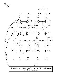
[0032] Referring to FIG. 1, a particular illustrative embodiment of a
resistance based
memory is depicted and generally designated 100. The memory 100 includes a
reference circuit 102 having a first reference path 110 and a second reference
path 120.
The memory 100 also includes a representative bit-zero data path 130 and a
representative bit-one data path 140. The reference paths 110 and 120 and the
data
paths 130 and 140 are generally designated as having a sense amplifier portion
104 that
provides load elements to a memory cell portion 106 to generate an output
signal for
comparison at a second sense amplifier (not shown). In a particular
embodiment, the
memory 100 is a magnetoresistive random access memory (MRAM), a phase-change
random access memory (PRAM), or a spin torque transfer MRAM (STT-MRAM).
[0033] The first reference path 110 includes a load device, such as a p-
channel metal
oxide semiconductor (PMOS) field effect transistor load 112. The PMOS load 112
is
coupled to a reference node (out ref) 160, which in turn is coupled to a clamp
transistor
114. A resistance RO 116 corresponding to a logic "zero" state of a resistance
based
memory element is coupled to the clamp transistor 114. A resistance based
memory
element is a device having a first resistance corresponding to a logic "one"
value and a
second resistance corresponding to a logic "zero" value, such as a magnetic
tunnel
junction (MTJ) device or a PRAM memory cell as illustrative, non-limiting
examples.
An access transistor 118 is coupled to the resistance RO 116.
[0034] The second reference path 120 includes a load device, such as a
PMOS load 122.
The PMOS load 122 is coupled to the reference node (out ref) 160, which in
turn is
coupled to a clamp transistor 124. A resistance R1 126 corresponding to a
logic "one"
CA 02720058 2010-09-28
WO 2009/131804 PCT/US2009/038924
6
state of a resistance based memory element is coupled to the clamp transistor
124. An
access transistor 128 is coupled to the resistance R1 126.
[0035] The representative bit-zero data path 130 includes a load device,
such as a
PMOS load 132. The PMOS load 132 is coupled to a reference node (out data0)
162,
which in turn is coupled to a clamp transistor 134. A resistance based memory
element
having a logic "zero" state is represented as a resistance RO 136, which is
coupled to the
clamp transistor 134. An access transistor 138 is coupled to the resistance RO
136.
[0036] The representative bit-one data path 140 includes a load device,
such as a PMOS
load 142. The PMOS load 142 is coupled to a reference node (out datal) 164,
which in
turn is coupled to a clamp transistor 144. A resistance based memory element
having a
logic "one" state is represented as a resistance R1 146, which is coupled to
the clamp
transistor 144. An access transistor 148 is coupled to the resistance R1 146.
[0037] Generally, corresponding components of each of the paths 110, 120,
130, 140
may have similar configurations and may operate in a substantially similar
manner.
Each of the clamp transistors 114, 124, 134, and 144 functions to limit
current and
voltage through the respective paths 110, 120, 130, and 140 based on a signal
Vclamp
144. Vclamp 144 represents a common gate voltage that enables the clamp
transistors
114, 124, 134, and 144 to function as clamping transistors. Each of the access
transistors 118, 128, 138, and 148 selectively allows current flow through the
respective
paths 110, 120, 130, and 140 based on a common signal VwL that represents a
common
gate voltage to the access transistors 118, 128, 138, and 148. Each of the
PMOS load
devices 112, 122, 132, and 142 has a gate terminal that is coupled to the out
ref node
160.
[0038] In a particular embodiment, a signal margin AV, such as a sense
amplifier
margin, corresponds to a difference between a voltage at the out datal node
164 and a
voltage at the out ref node 160 (AVi), or a difference between a voltage at
the out ref
node 160 and a voltage at the out data node 162 (AV0), whichever is smaller.
The
signal margin may be improved by increasing a difference between the voltage
at the
out datal node 164 and the voltage at the out data0 node 162. An iterative
method 170
to determine a value for Vclamp and a width of the PMOS loads 112, 122, 132,
and 142
based on one or more design constraints may enable a designer of the memory
100 to
CA 02720058 2010-09-28
WO 2009/131804 PCT/US2009/038924
7
adjust circuit parameters in a manner that satisfies design constraints while
enabling the
signal margin AV to approach a physically maximum value given the design
constraints.
[0039] Referring to FIG. 2, a block diagram of particular illustrative
embodiment of a
system to determine resistance based memory circuit parameters is depicted and
generally designated 200. In a particular embodiment, the system 200 may be
configured to perform the iterative method 170 depicted in FIG. 1. The system
200
includes a device 202 having at least one processor 204 and a memory 206 that
is
accessible to the processor 204. The memory 206 includes media that is
readable by the
processor 204 and that stores data and program instructions that are
executable by the
processor 204, including automated design tool instructions 208, parameter
iteration
instructions 210, circuit simulation instructions 212, and a data file 218
that includes
parameter values 214 and a circuit layout 216. An input device 230 and a
display 240
are coupled to the device 202. In a particular embodiment, the input device
230 may
include a keyboard, a pointing device, a touch screen, a speech interface,
another device
to receive user input, or any combination thereof
[0040] In a particular embodiment, the automated design tool instructions
208 are
executable by the processor 204 to enable a user to design a circuit via the
input device
230 and the display 240, and to store data associated with elements and
connections of
the circuit as the circuit layout 216. One or more device or circuit
parameters associated
with the circuit may be stored as parameter values 214. The circuit simulation
instructions 212 may be executable by the processor 204 to read data from the
data file
218 and to perform one or more simulations to model a behavior of the circuit.
The
parameter iteration instructions 210 may be executable by the processor 204 to
cause
the processor 204 to perform iterative adjustments of parameters of one or
more circuits,
such as a circuit of the memory 100 depicted in FIG. 1, in conjunction with
the circuit
simulation instructions 212.
[0041] In an illustrative embodiment, the parameter iteration instructions
210 are
executable by the processor 204 to receive a first input of a first parameter
based on a
first predetermined design constraint of a resistance based memory circuit.
The
parameter iteration instructions 210 are executable by the processor 204 to
receive a
second input of a second parameter based on a second predetermined design
constraint
CA 02720058 2010-09-28
WO 2009/131804 PCT/US2009/038924
8
of the resistance based memory circuit. For example, the first and second
parameters
may include a process parameter, such as a resistance value associated with
one or more
of the memory elements 116, 126, 136, and 146, or a device parameter, such as
a width
of the clamp transistors 114, 124, 134, and 144, a width of the access
transistors 118,
128, 138, and 148, a gate voltage Vclamp applied to the clamp transistors 114,
124, 134,
and 144, and a width of the PMOS loads 112, 122, 132, and 142, depicted in
FIG. 1.
Illustrative examples of predetermined design constraints include a logic
"zero"
resistance value of a magnetic tunnel junction (MTJ) device to substantially
maximize
signal margin, a read current limitation of a MTJ device in a bit "one" state
to prohibit a
read disturbed write where a read operation writes a value to the MTJ device,
a
maximum bitline voltage VBL at the memory cell portion, such at the node BL
datal of
FIG. 1, to maintain a reasonable value of a magnetic resistance (MR) ratio of
a MTJ
device, and a maximum transistor size of a sense amplifier portion that
satisfies a
bitline-to-input/output multiplexer scheme.
[0042] The parameter iteration instructions 210 may also be executable by
the processor
204 to perform an iterative methodology to adjust at least one circuit
parameter of a
sense amplifier portion of the resistance based memory circuit by selectively
adjusting a
physical property of the at least one circuit parameter to achieve a desired
sense
amplifier margin value without changing the first parameter or the second
parameter.
For example, the iterative methodology may begin with determining an initial
value of a
gate voltage of a clamp transistor of the sense amplifier portion, such as
Vclamp of FIG.
1, and an initial value of a width of a load transistor of the sense amplifier
portion, such
as a width of the PMOS loads 112, 122, 132, and 142 of FIG. 1, that together
result in a
substantially maximum sense amplifier margin value given the first parameter
and the
second parameter. A current of the sense amplifier portion may be determined
using the
initial value of the gate voltage and the initial value of the width of the
load transistor,
and the current of the sense amplifier portion may be compared to a
predetermined
current threshold. A bitline voltage VBL at the memory cell portion may also
be
determined and compared to a predetermined bitline voltage threshold (VBLmax).
[0043] A physical property, such as a gate voltage or a load transistor
width, may be
selectively adjusted when the current exceeds the predetermined current
threshold or the
bitline voltage exceeds the predetermined voltage threshold by determining a
reduced
CA 02720058 2010-09-28
WO 2009/131804 PCT/US2009/038924
9
gate voltage and determining a second width of the load transistor that
results in a
substantially maximum sense amplifier margin value given the first parameter,
the
second parameter, and the reduced gate voltage. A revised current of the sense
amplifier portion may also be determined using the reduced gate voltage and
the second
width of the load transistor. This process may be repeated, by reducing the
gate voltage
and re-determining the load transistor width, until a current through the
circuit does not
exceed the threshold and the bitline voltage does not exceed the predetermined
bitline
voltage threshold.
[0044] The parameter iteration instructions 210 may also be executable by
the processor
204 to store a value associated with the physical property after the desired
sense
amplifier margin is achieved given the predetermined first and second design
constraints. For example, one or more values associated with the physical
property,
such as the width of the PMOS loads 112, 122, 132, and 142, the voltage
applied to the
clamp transistors 114, 124, 134, and 144, other values associated with
physical
properties of circuit elements, or any combination thereof, may be stored with
the
parameter values 214. As another example, the data file 218 may be output to
represent
a circuit design of the resistance based memory circuit having the desired
sense
amplifier margin.
[0045] Although depicted as separate components, the automated design tool
instructions 208, the parameter iteration instructions 210, the circuit
simulation
instructions 212, or any combination thereof, may be integrated into a single
software
package or software applications that are compatible to interoperate with each
other. As
an illustrative, non-limiting example, the automated design tool instructions
208 and the
circuit simulation instructions 212 may be portions of a commercial computer-
aided
design (CAD) tool, and the parameter iteration instructions 210 may be
implemented as
scripts or other instructions compatible to be used with the commercial CAD
tool.
[0046] Referring to FIG. 3, a diagram of a particular illustrative
embodiment of current-
voltage characteristics of a clamp device of a resistance based memory is
depicted and
generally designated 300. The clamp device may be a clamp transistor, such as
the
clamp transistors 134 or 144 depicted in FIG. 1. A first curve 302 represents
a current
through the clamp transistor when a resistance based memory element is in a
logic
"zero" state, such as a current through RO 136 or RO 116, and a second curve
304
CA 02720058 2010-09-28
WO 2009/131804 PCT/US2009/038924
represents a current through the clamp transistor when a resistance based
memory
element is in a logic "one" state, such as a current through R1 146 or R1 126.
[0047] In a particular embodiment, a resistance based memory element
consists of a
resistance and an access transistor. The access transistor can be modeled as a
resistance,
R011 accessT125 if the access transistor operates in the linear region. Thus,
an access
transistor characteristic can be combined with resistance characteristic. For
example,
referring to FIG. 4, a diagram of a particular illustrative embodiment of
current-voltage
characteristics of a combined resistance and access transistor is depicted and
generally
designated 400. A first line 402 represents a current though the resistance
based
memory element in a logic "zero" state, and a second line 404 represents a
current
though the resistance based memory element in a logic "one" state.
[0048] Referring to FIG. 5, a diagram of a particular illustrative
embodiment of
current-voltage characteristics of a clamp device having characteristics
depicted in FIG.
3 serially coupled to a resistance based memory element having characteristics
depicted
in FIG. 4 is depicted and generally designated 500. A first curve 502
represents a
current, such as 10 or heft) of FIG. 1, through the clamp transistor and the
resistance
based memory element in a logic "zero" state, without the PMOS load 132 or 112
of
FIG. 1. A second curve 504 represents a current, such as Ii or Irefl of FIG.
1, though
the clamp transistor and the resistance based memory element in a logic "one"
state,
without the PMOS load 142 or 122 of FIG. 1. Both the first and the second
curve 502
and 504 exhibit a steep linear region at low voltages and a relatively flat
saturation
region at larger voltages.
[0049] Generally, in a system exhibiting the behavior depicted in FIG. 5,
such as the
memory 100 of FIG. 1, a signal margin AV may be increased by (1) reducing the
slope
of the first and second curves 502 and 504 in the saturation region, (2)
increasing a
difference between the current represented by the first curve 502 and the
current
represented by the second curve 504 in the saturation region, and (3)
increasing a size of
the saturation region of the first and second curves 502 and 504.
[0050] The slope of the first and second curves 502 and 504 in the
saturation region
may be reduced by decreasing a gate-source voltage (VGS clamp) of the clamp
transistor
CA 02720058 2010-09-28
WO 2009/131804 PCT/US2009/038924
11
since slope ocl/ .1.0 oc I 0C VG. Using the clamp transistor 144 of FIG. 1 as
an illustrative
example,
[0051] VGS clamp ¨ VClamp ¨ VBL ¨ VClamp ¨ I(RMTJ + R011 accessTR)
[0052] where VBL is a voltage at a node BL datal coupled to the source
terminal of the
clamp transistor 144 and to the resistance R1 146, I is a current through the
resistance
R1 146, RMTJ is the resistance R1 146 where the resistance based memory device
is a
magnetic tunneling junction (MTJ) device, and Ron accessTR represents a
resistance of the
access transistor 148. VGS clamp decreases with increasing RMTJ.
[0053] The slope of the first and second curves 502 and 504 in the
saturation region
may also be reduced by decreasing a size (W) and a gate voltage (VG) of the
clamp
transistor to increase an output resistance .1.0 oc 1/I oc 1/W.
[0054] The difference between the current represented by the first curve
502 and the
current represented by the second curve 504 in the saturation region (Al) may
be
increased by adjusting a value of the memory element (for example, RMTJ) to be
closer
to an optimal value Ropt. A difference between the current represented by the
first curve
502 and the current represented by the second curve 504 in the saturation
region may be
increased by increasing a size (W) and a gate voltage (VG) of the clamp
transistor.
[0055] The saturation region of the first and second curves 502 and 504
may be
increased by decreasing a gate voltage (VG) of the clamp transistor and
increasing a size
(W) of the clamp transistor to keep current (I) unchanged:
[0056] (VGS - Vt)a z VW, VG ¨ Vt < VD
[0057] where VG is a gate voltage of the clamp transistor, Vt is a
threshold voltage of
the clamp transistor, and VD is a drain voltage of the clamp transistor.
[0058] Therefore, the signal margin AV may be adjusted by varying RMTJ, as
well as the
width W and gate voltage VG of the clamp transistor. As RMTJ increases, the
signal
margin AV also increases. However, when RMTJ increases beyond a certain value
Ropt,
an output resistance of the clamp transistor and a load transistor (such as
the PMOS load
142 of FIG. 1) increases, but the saturation region current difference Al
decreases.
Thus, the signal margin AV increases with RMTJ but is saturated for large
RMTJ.
CA 02720058 2010-09-28
WO 2009/131804 PCT/US2009/038924
12
[0059] The size and gate voltage for the clamp transistor also affect the
signal margin
AV: small size and low voltage results in a large output impedance, reducing a
slope in
the saturation region; large size and high voltage increases the saturation
region current
difference Al; and large size and low voltage results in a large saturation
region.
[0060] FIGs. 6 and 7 illustrate effects of clamp transistor width and gate
voltage of a
clamp transistor on the signal margin AV. Referring to FIG. 6, a diagram of a
particular
illustrative embodiment of characteristics of a resistance based memory with a
varying
gate voltage VG of a clamp device is depicted and generally designated 600. A
first
curve 602 represents a size of a clamp device to maximize a voltage difference
AVo
between a reference and a logic "zero" state of a resistance based memory
element. The
size of the clamp device is illustrated at the left axis as a width of a NMOS
clamp
transistor such as the clamp transistor 144 of FIG. 1. A second curve 604
represents the
voltage difference AVo. The voltage difference AV is illustrated at the right
axis as a
voltage difference between the out data node 162 and the out ref node 160 of
FIG. 1.
[0061] FIG. 6 depicts, for each given value of the gate voltage VG, a
maximum
simulated voltage difference AV attained by varying clamp size, and the
particular
clamp size that resulted in the maximum simulated AVo. Values of the maximum
simulated voltage difference AV over a range of values of the gate voltage VG
are
interpolated as the second curve 604, and values of the clamp size that
resulted in the
maximum simulated AV are interpolated as the first curve 602.
[0062] Similarly, FIG. 7 depicts a diagram 700 of a particular
illustrative embodiment
of characteristics of a resistance based memory with a varying size of a clamp
device.
A first curve 702 represents a gate voltage VG of a clamp device to maximize a
voltage
difference AV between a reference and a logic "zero" state of a resistance
based
memory element. The gate voltage VG is illustrated at the left axis as a gate
voltage of
an NMOS clamp transistor such as the clamp transistor 144 of FIG. 1. A second
curve
704 represents the voltage difference AVo. The voltage difference AV is
illustrated at
the right axis as a voltage difference between the out ref node 160 and the
out data
node 162 of FIG. 1.
[0063] FIG. 7 depicts, for each given value of a clamp transistor width, a
maximum
simulated AV attained by varying a clamp gate voltage VG, and the gate
voltage that
CA 02720058 2010-09-28
WO 2009/131804 PCT/US2009/038924
13
resulted in the maximum simulated AVo. Values of the maximum simulated voltage
difference AV over a range of clamp sizes are interpolated as the second
curve 704, and
values of the gate voltage VG of the clamp transistor that resulted in the
maximum
simulated AV are interpolated as the first curve 702. For comparison
purposes,
simulated data represented in FIG. 6 was generated using the same circuit
parameters as
the simulated data represented in FIG. 7, except as noted above.
[0064] Comparing values of the first curve 602 of FIG. 6 (clamp size
producing
maximum AV0) to corresponding clamp sizes in FIG. 7 illustrates that, for a
particular
clamp size, a maximum simulated AV in FIG. 6 may be approximately equal to a
maximum simulated AV in FIG. 7. For example, a clamp size of 2.6 um
corresponds
to AV of 0.133 in FIG. 6 (at VG=0.88V), while a clamp size of 2.6 um
corresponds to
AV of approximately 0.135 in FIG. 7. Similarly, a clamp size of 3.7 um
corresponds
to AV of 0.138 in FIG. 6 (at VG=0.86V), while a clamp size of 3.7 um
corresponds to
AV of approximately 0.139 in FIG. 7, and a clamp size of 5.4 um corresponds
to AVo
of 0.142 in FIG. 6 (at VG=0.84V), while a clamp size of 5.4 um corresponds to
AV of
approximately 0.144 in FIG. 7.
[0065] Because both methods of adjusting parameters to achieve a
substantially
maximum signal voltage difference AV depicted in FIGs. 6 and 7 may provide
similar
results, a preference of parameter adjustment may be determined based on
additional
criteria. For example, a constraint on the clamp size may generally be harder
than a
constraint on the clamp gate voltage VG. In addition, controlling the clamp
gate voltage
VG may achieve a higher signal margin during parameter adjustment when a
current of a
logical "one" state exceeds a current threshold. Thus, determining the clamp
gate
voltage VG to substantially maximize the signal margin AV with a fixed clamp
size is
generally preferred.
[0066] Referring to FIG. 8, a diagram of a particular illustrative
embodiment of a load
portion of a circuit associated with a reference cell of a resistance based
memory device
is depicted and generally designated 800. The load portion includes a first
PMOS
transistor 812 that has a first terminal coupled to a supply Vdd and a second
terminal
coupled to a reference (out ref) node 860. A second PMOS transistor 822 has a
first
terminal coupled to the supply Vdd and a second terminal coupled to the out
ref node
860. A gate terminal of each of the first PMOS transistors 812 and 822 is
coupled to the
CA 02720058 2010-09-28
WO 2009/131804 PCT/US2009/038924
14
reference output node (out ref) 860. In an illustrative embodiment, the PMOS
transistors 812 and 822 and the out ref node 860 may correspond to the PMOS
load
devices 112 and 122 and to the out ref node 160, respectively, depicted in
FIG. 1.
Operation of the load portion 800 is illustrated in the load-line diagrams of
FIGs. 9-10.
[0067] Referring to FIG. 9, diagrams of a particular illustrative
embodiment of current-
voltage characteristics of a load device portion of a circuit associated with
a reference
cell of a resistance based memory device are depicted. FIG. 9(a) includes a
curve 902
that depicts a diode-like behavior of a current I top through the PMOS
transistors 812
and 822 of FIG. 8 as a function of source-to-drain voltage, VSD = Vdd ¨ Vout,
where Vout
is a voltage of the out ref node 860. Fig. 9(b) depicts a curve 904
corresponding to the
current through the PMOS transistors 812 and 822 of FIG. 8 as a function of
Vout = Vdd -
VsD. In a particular embodiment, I top corresponds to Iref of FIG. 1.
[0068] Referring to FIG. 10, a particular illustrative embodiment of a
load line
characteristic of the reference circuit 102 of FIG. 1 graphically illustrates
an operating
point of the reference circuit 102. A first curve 1002 illustrates a first
reference current
heft) through the logic "zero" reference path 110 including the access
transistor 118, the
memory element 116, and the clamp transistor 114, of FIG. 1 without the PMOS
load
112. A second curve 1004 illustrates a second reference current Irefl through
the logic
"one" reference path 120 including the access transistor 128, the memory
element 126,
and the clamp transistor 124, of FIG. 1 without the PMOS load 122. In a
particular
embodiment, the first curve 1002 and the second curve 1004 correspond to the
curves
502 and 504 of FIG. 5, respectively. A third curve 1006 illustrates an
arithmetic mean
of heft) and Irefl, given as (heft) + Irefl)/2. A fourth curve 1008
corresponds to the
curve 904 of FIG. 9(b) and illustrates the current Iref through the PMOS load
122 or
112 as a function of a voltage at the out ref node 160 (Vout).
[0069] Applying Kirchhoff s Current Law at the out ref node 160 of FIG. 1,
the sum of
a current Iref through the PMOS load 112 and the current Iref through the PMOS
load
122 equals the sum of first reference current heft) and the second reference
current Irefl,
so that Iref = 1/2 (Irefl + Iref2). Thus, an intersection 1010 of the third
curve 1006 and
the fourth curve 1008 indicates an operating point the reference circuit 102
of FIG. 1.
CA 02720058 2010-09-28
WO 2009/131804 PCT/US2009/038924
[0070] Referring to FIG. 11, a diagram of a particular illustrative
embodiment of a load
portion of a circuit associated with a data cell of a resistance based memory
device is
depicted and generally designated 1100. The load portion includes a first PMOS
transistor 1112 that has a first terminal coupled to a supply Vdd and a second
terminal
coupled to a data output (out data0) node 1162. A second PMOS transistor 1122
has a
first terminal coupled to the supply Vdd and a second terminal coupled a data
output
(out data0) node 1164. A gate terminal of each of the first PMOS transistors
1112 and
1122 is coupled to a reference output node (out ref). In an illustrative
embodiment, the
PMOS transistors 1112 and 1122 and correspond to PMOS load devices 132 and 142
of
the bit-zero data path 130 and the bit-one data path 140 of FIG. 1,
respectively, and the
out _data0 node 1162 and the out datal node 1164 correspond to the nodes 162
and 164
of FIG. 1, respectively. The reference output node (out ref) may be provided
by a
reference circuit, such as the out ref node 160 of FIG. 1, as graphically
illustrated in
FIG. 10. Operation of the load portion 1100 is illustrated in the load-line
diagrams of
FIGs. 12-14.
[0071] Referring to FIG. 12, diagrams of a particular illustrative
embodiment of
current-voltage characteristics of a load device portion of a circuit
associated with a data
cell of a resistance based memory device are depicted and generally designated
1200.
FIG. 12(a) includes a curve 1202 that depicts a current-voltage characteristic
of the
PMOS transistors 1112 or 1122 of FIG. 11 as a function of source-to-drain
voltage, VSD
= Vdd ¨ Vout, where Vout is a voltage at the out data0 node 1162 or the out
datal node
1164, respectively. Fig. 12(b) depicts a curve 1204 corresponding to the
current
through the PMOS transistor 1112 or 1122 of FIG. 11 as a function of Vout =
Vdd - Vsp.
[0072] Referring to FIG. 13, a particular illustrative embodiment of load
line
characteristics graphically illustrate operating points of the bit-zero path
130 and the bit-
one path 140 of FIG. 1. A first curve 1302 illustrates a first current 10
through the bit-
zero path 130 including the access transistor 138, the memory element 136, and
the
clamp transistor 134, of FIG. 1 without the PMOS load 132. A second curve 1304
illustrates a second current Ii through the bit-one path 140 including the
access
transistor 148, the memory element 146, and the clamp transistor 144 of FIG. 1
without
the PMOS load 142. In a particular embodiment, the first curve 1302 and the
second
curve 1304 correspond to the curves 502 and 504 of FIG. 5, respectively. A
third curve
CA 02720058 2010-09-28
WO 2009/131804 PCT/US2009/038924
16
1306 corresponds to the curve 1204 of FIG. 12(b) and illustrates current
through the
PMOS load 132 or 142 of FIG. 1 as a function of a voltage Vout at the out
data0 node
162 or out datal node 164, respectively.
[0073] A first intersection 1310 of the first curve 1302 and the third
curve 1306
indicates an operating point when a logic "zero" value is stored at a
resistance based
memory element, such as an operating point of the bit-zero path 130 of FIG. 1.
A
second intersection 1320 of the second curve 1304 and the third curve 1306
indicates an
operating point when a logic "one" value is stored at a resistance based
memory element,
such as an operating point of the bit-one path 140 of FIG. 1.
[0074] FIG. 14 graphically depicts operational parameters associated with
the load line
characteristics of FIGs. 10 and 13. A first curve 1402 illustrates a first
current 10
through the bit-zero path 130 or lief through the first reference path 110 of
FIG. 1,
including the access transistor 138 or 118, the memory element 136 or 116, and
the
clamp transistor 134 or 114, without the PMOS load 132 or 112, respectively,
referred
to as 'logic "zero" bottom-side circuit.' A second curve 1404 illustrates a
second
current Ii through the bit-one path 140 or Irefl through the second reference
path 120,
including the access transistor 148 or 128, the memory element 146 or 126, and
the
clamp transistor 144 of 124 without the PMOS load 142 or 122, referred to as
'logic
"one" bottom-side circuit.'
[0075] A third curve 1406 illustrates current through the PMOS load 132 or
142 as a
function of a voltage at the out data0 node 162 or out datal node 164,
respectively,
referred to as the "top-side data circuit." A fourth curve 1408 illustrates a
current Iref
through the PMOS load 112 or 122 of the reference circuit 102 of FIG. 1,
referred to as
the "top-side reference circuit," as a function of a voltage at the out ref
node 160, and in
a particular embodiment may correspond to the curve 904 of FIG. 9(b).
[0076] A first intersection 1410 of the first curve 1402 and the third
curve 1406
indicates a voltage (Vout data0 1414) at the out data0 node 162 and a current
(10 1412)
corresponding to an operating point of the bit-zero path 130 of FIG. 1. A
second
intersection 1420 of the second curve 1404 and the third curve 1406 indicates
a voltage
(Vout datal 1424) at the out datal node 164 and a current (I1 1422)
corresponding to
an operating point of the bit-one path 140 of FIG. 1. A third intersection
1430 of the
CA 02720058 2010-09-28
WO 2009/131804 PCT/US2009/038924
17
third curve 1406 and the fourth curve 1408 indicates a voltage (Vout ref 1434)
at the
out ref node 160 and a current (Iref 1432) at an operating point of the
reference circuit
102. The operating point of the reference circuit 102 indicated by the third
intersection
1430 is equivalent to the operating point determined by the technique
discussed with
respect to FIG. 10.
[0077] A voltage difference AV between the voltage at the out ref node
160
(Vout ref) and the voltage at the out data node 162 (Vout data0) indicates a
tolerance
of the memory 100 to noise or to process variation in detecting a logic "zero"
value
stored at a resistance based memory element. A voltage difference AV' between
the
voltage at the out datal node 164 (Vout datal) and the voltage at the out ref
node 160
(Vout ref) indicates a tolerance of the memory 100 to noise or to process
variation in
detecting a logic "one" value stored at a resistance based memory element. The
signal
margin of the memory 100 is equal to AV , as the smaller of AV and AV'.
Similarly,
current differences AL and AIi correspond to differences between Iref and IO,
and Ii
and Iref, respectively.
[0078] Referring to FIG. 15, a diagram of a first particular illustrative
embodiment of
characteristics of the memory 100 of FIG. 1 is depicted and generally
designated 1500.
A first curve 1502 and a second curve 1504 illustrate current-voltage (I-V)
characteristics for the logic "zero" bottom-side circuit and the logic "one"
bottom-side
circuit, respectively. A first set of load lines 1520 and 1522 correspond to I-
V
characteristics of the top-side reference circuit and the top-side data
circuit, respectively,
with a first width of the PMOS transistors 112, 122, 132, and 142. A second
set of load
lines 1540 and 1542 correspond to I-V characteristics of the top-side
reference circuit
and the top-side data circuit, respectively, where the PMOS transistors 112,
122, 132,
and 142 have a second width that is larger than the first width.
[0079] The first set of load lines 1520 and 1522 demonstrate that the PMOS
transistors
having the first width restrict current so that the clamp devices operate in
the linear
region, resulting in an undesirably small AV. The second set of load lines
1540 and
1542 demonstrate that the PMOS transistors having the second width allow
enough
current to flow to enable both of the clamp devices to operate in the
saturation region.
An intersection 1550 of the load lines 1540 and 1542 indicates a voltage at
the out ref
node 160 of FIG. 1. An intersection 1552 of the load line 1540 and the first
curve 1502
CA 02720058 2010-09-28
WO 2009/131804 PCT/US2009/038924
18
indicates a bit "zero" output voltage, and an intersection 1554 of the load
line 1540 and
the second curve 1504 indicates a bit "one" output voltage. Both of the
intersections
1552 and 1554 indicate that the clamp devices are operating in the saturation
region,
although the intersection 1552 corresponding to the bit "zero" state is
within, but at the
margin of, the saturation region.
[0080] Referring to FIG. 16, a diagram of a second particular illustrative
embodiment of
characteristics of the memory 100 of FIG. 1 is depicted and generally
designated 1600.
A first curve 1602 and a second curve 1604 illustrate current-voltage (I-V)
characteristics for the logic "zero" bottom-side circuit and the logic "one"
bottom-side
circuit, respectively. Load lines 1640 and 1642 correspond to I-V
characteristics of the
top-side reference circuit and the top-side data circuit, respectively. An
intersection
1650 of the load lines 1640 and 1642 indicates a voltage at the out ref node
160. An
intersection 1652 of the load line 1640 and first curve 1602 indicates a bit
"zero" output
voltage, and an intersection 1654 of the load line 1640 and the second curve
1604
indicates a bit "one" output voltage. Both of the intersections 1652 and 1654
indicate
that the clamp devices are operating in the saturation region. However, the
PMOS load
has a lowered output resistance ro than as illustrated in FIG. 15, as
demonstated by a
slope of the load line 1640.
[0081] FIGs. 17-19 illustrate a particular illustrative embodiment of an
operation of a
resistance based memory having a logic "one" current exceeding a current
threshold
(FIG. 17), and the resistance based memory after the logic "one" current has
been
reduced by reducing a gate voltage of a clamp transistor (FIG. 18) or by
reducing a
width of the clamp transistor (FIG. 19), and the corresponding signal margins
that
result.
[0082] Referring to FIG. 17, a diagram of a particular illustrative
embodiment of
characteristics of a resistance based memory device having a current exceeding
a
threshold value is depicted and generally designated 1700. A first curve 1702
and a
second curve 1704 illustrate current-voltage (I-V) characteristics for the
logic "zero"
bottom-side circuit and the logic "one" bottom-side circuit, respectively.
Load lines
1740 and 1742 correspond to I-V characteristics of of the top-side reference
circuit and
the top-side data circuit, respectively. A region 1750 generally indicates the
operating
point of the bit-one data path 140. In a particular embodiment, a current
associated with
CA 02720058 2010-09-28
WO 2009/131804 PCT/US2009/038924
19
the logic "one" state (Ii) has a value of approximately nineteen microamps
(uA),
exceeding a threshold current of fifteen uA as an illustrative, non-limiting
example of a
threshold current. The threshold current Imax may indicate a maximum allowed
current
to prevent invalid write commands during read operations.
[0083] The voltage difference AV between the intersection of the load
lines 1740 and
1742 and the intersection of the first curve 1702 and the load line 1740 is
approximately
267 millivolts (mV). The voltage difference AVi between the intersection of
the first
curve 1702 and the load line 1740 and the intersection of the load lines 1740
and 1742
is approximately 298 millivolts (mV). The signal margin, determined as the
lesser of
AV and AVi, is thus given by AVo and has a value 267 mV.
[0084] Referring to FIG. 18, a diagram of a particular illustrative
embodiment of
characteristics of the resistance based memory device of FIG. 17 having a
reduced gate
voltage of a clamp device is depicted and generally designated 1800. Starting
from the
embodiment of FIG. 17, to reduce current in the bit "one" state to a value
less than or
equal to Imax (15uA), a gate voltage VG of a clamp device is first reduced,
after which a
width of the PMOS transistors 112, 122, 132 and 142 is reduced to achieve a
substantially maximal value of AV of 262 mV at a bit "one" current of fifteen
uA. As
illustrated, AVi is 297mV, and the signal margin is thus given by AV and has
a value
267 mV.
[0085] Referring to FIG. 19, a diagram of a particular illustrative
embodiment of
characteristics of the resistance based memory device of FIG. 17 with a
reduced width
of a clamp device is depicted and generally designated 1900. Starting from the
embodiment of FIG. 17, to reduce current in the bit "one" state to a value
less than or
equal to Imax (15uA), a width of the clamp device is first reduced, after
which a width of
the PMOS transistors 112, 122, 132 and 142 is reduced to achieve a
substantially
maximal value of AV of 241 mV at a bit "one" current of fifteen uA. As
illustrated, the
value of AVi is 274 mV, and the signal margin is thus given by AV and has a
value of
241 mV. The signal margin of FIG. 19 is smaller, and thus less desirable, than
the
signal margin of FIG. 18, primarily because a larger saturation region results
from
reducing VG to lower Ii to Imax than from reducing clamp size to lower Ii to
'max.
CA 02720058 2010-09-28
WO 2009/131804 PCT/US2009/038924
[0086] As illustrated in FIGs. 3-19, parameters of a resistance based
memory such as
the memory 100 of FIG. 1 may be selectively adjusted in a manner designed to
produce
a largest achievable signal margin, given as the smaller of AV and ANL Other
considerations in determining device parameters include the recognition that a
large
resistance of the memory element causes a high current density. In addition, a
maximum data 1 read current should be low enough to prevent invalid data
writing
during a read operation, and a bitline voltage should not exceed a threshold
bitline
voltage (VBLmax) to maintain reasonable values of a magnetic resistance (MR)
ratio.
[0087] Referring to FIG. 20, a flow diagram of a first particular
embodiment of a
method of determining a set of parameters of a resistance based memory circuit
is
depicted and generally designated 2000. As illustrative examples, the
resistance based
memory circuit may include a magnetoresistive random access memory (MRAM), a
phase-change random access memory (PRAM), a spin torque transfer MRAM (STT-
MRAM), or other resistance based memory devices.
[0088] At 2002, a first parameter is selected based on a first
predetermined design
constraint of the resistance based memory circuit. Moving to 2004, a second
parameter
is selected based on a second predetermined design constraint of the
resistance based
memory circuit. In a particular embodiment, the first predetermined design
constraint
may include a process parameter, such as a resistance value associated with a
resistance-
based memory element. Process design constraints may not be variable or may be
difficult to satisfy because the process parameter may be fixed or less
flexible than
circuit design parameters. The second parameter may include a circuit design
parameter
such as a maximum device size, or a maximum transistor width due to a physical
spacing limit. For example, a maximum transistor size of a sense amplifier
portion may
be limited due to a bitline-to-input/output multiplexer scheme.
[0089] Continuing to 2006, an iterative methodology is performed to adjust
at least one
circuit parameter of a sense amplifier portion of the resistance based memory
circuit by
selectively assigning and adjusting a physical property of the at least one
circuit
parameter to achieve a desired sense amplifier margin value without changing
the first
parameter and the second parameter. Physical properties that may be adjusted
include
transistor dimensions and gate bias voltages, as illustrative examples. In a
particular
embodiment, performing the iterative methodology includes adjusting the
physical
CA 02720058 2010-09-28
WO 2009/131804 PCT/US2009/038924
21
property to increase a sense amplifier margin at 2008. The desired sense
amplifier
margin may be a predetermined margin value, or may be a substantially maximum
amplifier signal margin given the first and second predetermined design
constraints.
[0090] The circuit design parameter may include a width of a load
transistor that is
coupled to operate as a load. For example, the circuit design parameter may
include a
width of the load devices 112, 122, 132, and 134 depicted in FIG. 1. The
circuit design
parameter may include a gate voltage of a clamp transistor within the sense
amplifier
portion of the memory circuit. For example, the circuit design parameter may
include a
value of Vclamp depicted in FIG. 1.
[0091] The clamp transistor may operate in a saturation mode and may limit
a current in
a data read path of a magnetic tunnel junction (MTJ) element of the resistance
based
memory circuit. In a particular embodiment, the reference cell includes a p-
channel
metal oxide semiconductor (PMOS) field effect transistor load coupled to the
clamp
transistor. The MTJ element may be coupled to the clamp transistor and further
coupled
to an access transistor. The resistance based memory circuit may further
include a data
cell having a second PMOS load, a second clamp transistor, a second MTJ
element, and
a second access transistor, such as the data paths 130 and 140 of FIG. 1.
[0092] Referring to FIG. 21, a diagram of a second particular embodiment
of a method
of determining a set of parameters of a resistance based memory circuit is
depicted and
generally designated 2100. A value of a resistance RMTJ of a magnetic tunnel
junction
memory element is set to a predetermined value RMTJ opt, at 1502. In a
particular
embodiment, RMTJ opt is the optimal RO value to maximize the signal margin. At
2104,
a width of a clamp transistor W
naamp of a spin torque transfer magnetoresistive random
access memory (STT-MRAM) is set to a value W
nclamp max. Wnclamp max may be a
predetermined design constraint that is selected to be substantially a largest
width that
satisfies a spacing limit of the STT-MRAM. For example, the spacing limit may
be
determined by a bitline-to-input/output multiplexing scheme of the STT-MRAM,
such
as 4:1 or 8:1, which limits a transistor width of a sense amplifier portion of
the STT-
MRAM. A signal margin AV may increase and saturate with an increase of the
width
of the clamp transistor, such as illustrated in FIG. 7, and the width of the
clamp
transistor may be selected based on the signal margin and an area limitation.
CA 02720058 2010-09-28
WO 2009/131804 PCT/US2009/038924
22
[0093] In addition, other parameters may be selected or otherwise
determined based on
predetermined constraints, such as a resistance RmTj of a magnetic tunnel
junction
(MTJ) of the STT-MRAM at a bit-zero state, a maximum read current 'max to
prevent
changing a bit-one state to a bit-zero state during a read operation of the
bit-one state,
other process and circuit design parameters, or any combination thereof In a
particular
example, one or more selected parameters may include process parameters
determined
by process technology, such as the resistance of the MTJ.
[0094] After the parameters are selected, an iterative methodology begins.
The iterative
methodology generally includes adjusting at least one circuit design parameter
of the
sense amplifier portion of the STT-MRAM by selectively adjusting a physical
property
of the at least one circuit design parameter to achieve a desired sense
amplifier margin
value, but without changing the previously determined parameters such as RmTj
or
Wnload affected by design constraints. Moving to 2106, initial values of a
gate voltage
VG of the clamp transistor and a width W
pload of a load transistor are determined to
substantially maximize a signal margin AV of the STT-MRAM.
[0095] Continuing to 2108, a bit-one state current (I) of the MTJ is
compared to the
predetermined current threshold 'max and a voltage (VBL) of the bitline is
compared to a
predetermined voltage threshold VBLmax= At decision 2110, a determination is
made
whether the bit-one state current I is less than 'max and VBL is less than
VBLmax= When I <
'max and VBL < VBLmax, the method terminates at 2116. When I exceeds 'max or
VBL
exceeds VBLmax, processing advances to 2112 to begin iteratively reducing the
gate
voltage VG of the clamp transistor and determining the width W
pload of the load
transistor that results in a substantially maximum sense amplifier margin
given the gate
voltage VG. In the illustrative embodiment depicted in FIG. 21, in the case
where I is
equal to 'max Or VBL is equal to VBLmax, processing also advances to 2112,
although in
another embodiment processing may instead advance to 2116, where the method
terminates.
[0096] At 2112, the gate voltage VG is reduced. VG may be reduced by a
predetermined
amount or a calculated step size. After reducing VG, at 2114, a next value of
Wpload is
determined to substantially maximize AVo. Processing returns to 2108, where I
and VBL
are calculated using the values determined at 2112 and 2114.
CA 02720058 2010-09-28
WO 2009/131804 PCT/US2009/038924
23
[0097] The general dependence of AV on W
nclamp and VG illustrated in FIGs. 17-19
suggests that reducing the current I while maintaining a largest possible
signal margin,
given as the smaller of AV and AV', may be achieved by setting a largest
reasonable
Wnclamp and by iteratively reducing VG, and adjusting Wooad, until I is less
than 'max.
Circuit designs that are determined without following the design flows
discussed with
respect to FIGs. 1-21 may have local optimums in certain aspects, but may
suffer from
signal margin issues and low yields. At least a portion of the iterative
methodology
illustrated in FIGs. 20-21 may be performed by an automated design tool, such
as
described with respect to the system 200 of FIG. 2. One or more parameters,
physical
properties, or any combination thereof, may be assigned an initial value prior
to
performing the iterative methodology at the automated design tool, such as via
the input
device 230 or the data file 218 of FIG. 2. The design tool may perform the
iterations to
generate a circuit design that is substantially globally optimized for signal
margin, given
the accuracy of device models and simulation algorithms of the design tool,
and other
implementation factors such as step sizes and rounding errors.
[0098] Referring to FIG. 22, a block diagram of a particular illustrative
embodiment of
an electronic device including a resistance based memory circuit with
parameters
determined by an iterative methodology, as described herein, is depicted and
generally
designated 2200. The device 2200 includes a processor, such as a digital
signal
processor (DSP) 2210, coupled to a memory 2232 and also coupled to a
resistance
based memory circuit with parameters determined by an iterative methodology
2264. In
an illustrative example, the resistance based memory circuit with parameters
determined
by the iterative methodology 2264 includes the memory depicted in FIG. 1 and
has
circuit parameters determined using one or more of the methods of FIGs. 20 and
21,
using the device 202 of FIG. 2, or any combination thereof In a particular
embodiment,
the resistance based memory circuit with parameters determined by the
iterative
methodology 2264 includes a spin torque transfer magnetoresistive random
access
memory (STT-MRAM) memory device.
[0099] FIG. 22 also shows a display controller 2226 that is coupled to the
digital signal
processor 2210 and to a display 2228. A coder/decoder (CODEC) 2234 can also be
coupled to the digital signal processor 2210. A speaker 2236 and a microphone
2238
can be coupled to the CODEC 2234.
CA 02720058 2010-09-28
WO 2009/131804 PCT/US2009/038924
24
[00100] FIG. 22 also indicates that a wireless controller 2240 can be
coupled to the
digital signal processor 2210 and to a wireless antenna 2242. In a particular
embodiment, the DSP 2210, the display controller 2226, the memory 2232, the
CODEC
2234, the wireless controller 2240, and the resistance based memory circuit
with
parameters determined by the iterative methodology 2264 are included in a
system-in-
package or system-on-chip 2222. In a particular embodiment, an input device
2230 and
a power supply 2244 are coupled to the on-chip system 2222. Moreover, in a
particular
embodiment, as illustrated in FIG. 22, the display 2228, the input device
2230, the
speaker 2236, the microphone 2238, the wireless antenna 2242, and the power
supply
2244 are external to the on-chip system 2222. However, each can be coupled to
a
component of the on-chip system 2222, such as an interface or a controller.
[00101] Those of skill would further appreciate that the various
illustrative logical
blocks, configurations, modules, circuits, and algorithm steps described in
connection
with the embodiments disclosed herein may be implemented as electronic
hardware,
computer software, or combinations of both. To clearly illustrate this
interchangeability
of hardware and software, various illustrative components, blocks,
configurations,
modules, circuits, and steps have been described above generally in terms of
their
functionality. Whether such functionality is implemented as hardware or
software
depends upon the particular application and design constraints imposed on the
overall
system. Skilled artisans may implement the described functionality in varying
ways for
each particular application, but such implementation decisions should not be
interpreted
as causing a departure from the scope of the present disclosure.
[00102] The steps of a method or algorithm described in connection with the
embodiments disclosed herein may be embodied directly in hardware, in a
software
module executed by a processor, or in a combination of the two. A software
module
may reside in random access memory (RAM), flash memory, read-only memory
(ROM), programmable read-only memory (PROM), erasable programmable read-only
memory (EPROM), electrically erasable programmable read-only memory (EEPROM),
registers, hard disk, a removable disk, a compact disc read-only memory (CD-
ROM), or
any other form of storage medium known in the art. An exemplary storage medium
is
coupled to the processor such that the processor can read information from,
and write
information to, the storage medium. In the alternative, the storage medium may
be
CA 02720058 2013-09-06
74769-3129
integral to the processor. The processor and the storage medium may reside in
an
application-specific integrated circuit (ASIC). The ASIC may reside in a
computing
device or a user terminal. In the alternative, the processor and the storage
medium may
reside as discrete components in a computing device or user terminal.
[00103] The previous description of the disclosed embodiments is provided
to enable any
person skilled in the art to make or use the disclosed embodiments. Various
modifications to these embodiments will be readily apparent to those skilled
in the art,
and the generic principles defined herein may be applied to other embodiments
without
departing from the scope of the claims.