Note: Descriptions are shown in the official language in which they were submitted.
CA 02720162 2010-09-30
WO 2009/123999 PCT/US2009/038867
FEEDFORWARD LINEARIZATION OF RF POWER AMPLIFIERS
The inventive arrangements relate to methods for linearizing RF power
amplifiers, and more particularly to a method for providing an envelope
elimination
and restoration (EER) amplifier with enhanced linearity.
The migration of broadcast and other communications industries to
complex digital waveforms has necessitated a degree of amplifier linearity
that is
unprecedented. Concurrently, there is a continuing demand for amplifiers that
operate
more efficiently and offer reduced power consumption. In the case of large
transmitter installations, greater efficiency is important for reducing waste
heat and
costs. In other applications, such as that involving portable transceiver
equipment,
efficiency is important for reducing size, weight, and battery consumption.
One type of RF power amplifier which offers improved efficiency is
the envelope elimination and restoration (EER) amplifiers. EER amplifiers are
well
known in the art and can achieve very highly efficient conversion of DC energy
to RF
energy for complex waveforms having a varying envelope. They operate by
separately processing the envelope and phase information contained in a
modulated
input signal. The phase information is communicated to a power amplifier where
it is
amplified as a constant envelope signal. This permits such phase information
to be
amplified using highly efficient non-linear amplifiers. The envelope
information
contained in the input signal is restored to the phase information after the
signal has
been amplified.
Although highly efficient, EER amplifiers using Class E topologies are
known to have poor linearity. This poor linearity causes significant amounts
of signal
distortion. For example, such distortion often arises from pulse-width
modulator
circuits that are used to control the output envelope voltage, and from
switching non-
linearities which exist in the circuit used for amplifying the phase
information. The
nonlinearities cause spectral re-growth (out-of-band noise), which leads to
adjacent
channel interference. It also causes in-band distortion, which degrades the
bit-error
rate (BER) performance for digital modulation waveforms. In order to comply
with
CA 02720162 2010-09-30
WO 2009/123999
PCT/US2009/038867
FCC spectral masks, reduce BER, and achieve acceptable amplifier efficiency,
linearization is necessary.
Distortion associated with RF power amplifiers is often characterized
by means of an amplitude to amplitude (AM-to-AM) modulation curve and an
amplitude-to-phase (AM-to-PM) modulation curve. The AM-to-AM modulation
curve shows the RF power amplifier gain as a function of the input power. The
AM-
to-PM modulation curve shows the output phase variation of the RF power
amplifier
as a function of the input power. It will be appreciated that AM-to-AM
distortion and
AM-to-PM distortion can adversely affect the performance of an RF
communication
system. For example, such distortion can make it difficult to recover symbols
at a
receiving end of a communication link.
One well known method for improving the linearity of RF power
amplifiers is known as feedforward linearization. With feedforward
linearization, an
RF splitter is typically used to separate a source signal into two separate
signals.
These two signals include a amplifier input signal and a reference signal. The
amplifier input signal is provided to the amplifier as an input. A directional
RF
coupler is used to obtain a sample of the distorted output signal from the RF
power
amplifier. The reference signal and the sampled output from the directional
coupler
are communicated to separate inputs of a 180 hybrid RF signal combiner. The
180
hybrid RF hybrid combiner subtracts the reference signal from the distorted
amplifier
output. The resulting output from the combiner is an error signal. The error
signal is
subsequently amplified so as to scale the error signal to equal the power
level of any
distortion contained in the distorted output signal from the RF power
amplifier. The
error signal is then subtracted from the distorted output signal of the RF
power
amplifier to remove the distortion from the output signal.
Feedforward linearization is effective at improving amplifier linearity.
However, it has not been particularly practical for certain amplifier
applications. For
example, the relatively large magnitude of the error signal needed to improve
the
linearity of highly non-linear amplifiers can require a relatively high power
RF
amplifier for scaling the error signal. The necessity for such a relatively
high power
-2-
CA 02720162 2010-09-30
WO 2009/123999 PCT/US2009/038867
RF amplifier for scaling the error signal can reduce the overall efficiency of
the
amplifier system. Thus, feedforward linearization has been limited with regard
to its
usefulness as applied to highly non-linear amplifiers, such as the EER type
amplifier.
Another limitation of feedforward linearization concerns bandwidth.
In feedforward linearization systems, it is important for the error signal to
be a highly
accurate representation of the actual distortion produced by the RF power
amplifier.
A distorted error signal will not properly remove non-linearities from the
output of the
amplifier. However, in the case where the signals to be amplified are wideband
RF
signals inaccuracy of the error signal can occur. For example, such
inaccuracies can
result from amplitude and phase variations which exist across the operating
bandwidth of the RF components used to form and process the error signal. As
noted
above, such RF components can include RF signal splitters and 180 RF hybrid
combiner circuits.
The invention concerns an RF amplifier system incorporating
feedforward linearization. The system includes a digital multiplexer coupled
to a
digital waveform source. The digital multiplexer is configured to generate
first and
second instances of the digital data. A first data converting subsystem is
coupled to
the digital multiplexer for converting the first instance of the digital data
to analog
magnitude and phase signals defining the analog signal. An RF amplifier is
coupled
to the first data converting subsystem and is responsive to the magnitude and
phase
signals for generating a distorted RF output signal modulated by one or more
of the
magnitude and phase signals. A second data converting subsystem is configured
for
receiving the second instance of the digital data from the digital multiplexer
and
converting the second instance of the digital data to an analog RF reference
signal.
A feedforward linearization circuit is provided for reducing a distortion
of the RF amplifier. The distorted RF output signal and the analog RF
reference
signal are communicated to the feedforward linearization circuit. The
feedforward
linearization circuit includes a differential amplifier arranged for
generating an error
signal representing a difference between the distorted RF output signal and
the analog
RF reference signal. The feedforward linearization circuit also includes a
combiner
-3-
CA 02720162 2010-09-30
WO 2009/123999
PCT/US2009/038867
for combining the error signal with the distorted RF output signal for
removing a
distorted portion of the distorted RF output signal.
The RF amplifier system advantageously includes a digital data time
delay device coupled to the digital multiplexer. The digital time delay device
is
configured for selectively delaying the second instance of the digital data so
that the
distorted RF output signal and the analog RF reference signal can be time
aligned
when they are communicated to the differential amplifier.
The invention also includes a method for linearizing an output signal
of an RF amplifier. The method includes the steps of generating first and
second
instances of a digital data s(t) using a digital multiplexer. The method also
includes
converting the first instance of the digital data to analog magnitude and
phase signals.
A distorted RF output signal is generated by an RF amplifier responsive to the
magnitude and phase signals. The RF output signal is modulated by at least one
of
the magnitude and phase signals. The method further includes converting the
second
instance of the digital data to an analog RF reference signal. The method
continues
by reducing a distortion of the distorted RF output signal using a feedforward
linearization circuit. An error signal is generated by the feedforward
linearization
circuit. The error signal represents a difference between the distorted RF
output
signal and the analog RF reference signal. The method continues with the step
of
combining the error signal with the distorted RF output signal for removing a
distorted portion of the distorted RF output signal.
Embodiments will be described with reference to the following
drawing figures, in which like numerals represent like items throughout the
figures,
and in which:
Fig. 1 is a block diagram of a conventional RF power amplifier
arrangement which incorporates a feedforward system for improving the
linearity of
the RF power amplifier.
Fig. 2 is a block diagram that is useful for understanding an
arrangement for an RF power amplifier arrangement which incorporates an
improved
-4-
CA 02720162 2010-09-30
WO 2009/123999 PCT/US2009/038867
feedforward system for correcting non-linearities in an output of an RF power
amplifier.
The invention will now be described more fully hereinafter with
reference to accompanying drawings, in which illustrative embodiments of the
invention are shown. This invention, may however, be embodied in many
different
forms and should not be construed as limited to the embodiments set forth
herein. For
example, the present invention can be embodied as a method, a data processing
system, or a computer program product. Accordingly, the present invention can
take
the form as an entirely hardware embodiment, an entirely software embodiment,
or a
hardware/software embodiment.
The system described herein is intended for improving the linearity of
an RF power amplifier, and more particularly for improving the linearity of RF
power
amplifiers used to amplify broadband signals. As used herein, the term linear
and/or
linearity is used to describe the extent to which an RF amplifier is able to
produce an
amplified output signal which has a amplitude which is related to its input
signal by
some constant scaling factor over a defined dynamic operating range of the RF
amplifier. Similarly, with regard to phase, the term linear or linearity is
used to
describe the degree to which such an RF amplifier can produce an amplified
output
signal which has a phase which is related to its input signal by some constant
value
over a defined dynamic operating range of the RF amplifier. The dynamic
operating
range, as that term is used herein, includes an expected range of signal
amplitudes,
and anticipated signal bandwidth.
There is a continuing demand for amplifiers that operate more
efficiently with unprecedented levels of linearity. Certain types of
amplifiers, such as
envelope elimination and restoration (EER) amplifiers, are known to have very
high
operating efficiency. However, these same amplifiers are also known to have
poor
linearity. According to an embodiment of the invention, the linearity of such
amplifiers can be improved by using an improved feedforward linearization
technique.
-5-
CA 02720162 2012-11-06
Referring now to FIG. 1, there is shown a simplified block diagram of
an RF power amplifier system which incorporates a feedforward system for
improving the amplifier's linearity. In the RF power amplifier system, a
waveform
source 102 communicates a source RF signal to an RF power divider 104. The RF
power divider is conventionally used to split an RF source signal into two
separate
signals. Typically, each of these signals will have an RF power which is
approximately half that of the source RF signal. The two signals thus produced
include an amplifier input signal and a reference signal. The amplifier input
signal is
provided as an input to the RF power amplifier 106. A directional coupler 108
is
conventionally used to obtain a low power sample of the distorted output
signal from
the RF power amplifier 106.
The reference signal and the sampled output signal from the directional
coupler 108 are communicated to separate inputs of a 180 hybrid RF signal
combiner 114. The conventional 180 hybrid RF signal combiner subtracts the
reference signal from the distorted amplifier output signal. The resulting
output from
the 180 hybrid RF signal combiner 114 is an error signal. The error signal is
subsequently amplified in a linear error amplifier 116 so as to scale the
error signal.
In particular, the error signal is amplified so that its power level is
properly scaled to
equal the power level of any distortion contained in the distorted output
signal from
the RF power amplifier 106. The distorted output signal from the directional
coupler
is also communicated to a second directional coupler 110. In the second
directional
coupler 110, the error signal is combined with the distorted output signal in
a
subtraction operation. In particular, the RF error signal is subtracted from
the
distorted output signal of the RF power amplifier to remove the distortion
from the
output signal.
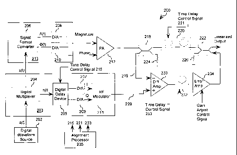
FIG. 2 shows a simplified block diagram of an RF power amplifier
system 200 with feedforward linearization incorporating a feedforward
arrangement
for removing non-linearities from the amplifier output. The arrangement shown
is
particularly useful for RF power amplifiers intended for use with wideband RF
signals.
-6-
CA 02720162 2010-09-30
WO 2009/123999 PCT/US2009/038867
Referring now to FIG. 2, the RF power amplifier system 200 includes a
digital waveform source 202 that generates digital data signal s(t). The
digital data
signal s(t) can be a conventional complex source signal. As used herein, a
complex
signal is any signal that is represented in terms of real and imaginary signal
components. For convenience in describing the present invention, the digital
data
signal can be understood to be comprised of digital data that represents an
analog
signal comprised of in phase (I) and quadrature (Q) component vectors (I/Q
component signal). Digital data of this type is well known in the art and
therefore
will not be described here in detail. Still, it should be understood that the
invention is
not limited in this regard. Instead, any other digital representation of a
complex time
varying analog signal can also be used. Regardless of the particular format
selected
for s(t) it should be understood that the digital waveform source 202
generates a
signal which can be considered ideal in that it is an exact digital
representation of the
desired analog signal. In particular the digital data signal s(t) lacks any
distortion
associated with conventional analog signal processing.
The digital waveform source 202 can be realized in computer
hardware, software, or a combination of hardware and software. In this regard
it
should be appreciated that the digital waveform source can be generated in one
digital
processing system, or in a distributed fashion where different processing
elements are
spread across several interconnected systems. Any kind of computer system, or
other
apparatus adapted for carrying out the methods described herein, is suited. A
typical
combination of hardware and software could be a general purpose computer
processor
or digital signal processor loaded with a computer program that controls the
computer
system such that it generates time varying digital representations of the I
and Q signal
components. Computer program or application in the present context means any
expression, in any language, code or notation, of a set of instructions
intended to
cause a system having an information processing capability to perform a
particular
function either directly or after either or both of the following a)
conversion to another
language, code or notation; b) reproduction in a different material form.
-7-
CA 02720162 2010-09-30
WO 2009/123999 PCT/US2009/038867
Referring again to FIG. 2, the digital data signal s(t) is communicated
to reference signal generator block 203. Reference signal generator block 203
includes at least one digital circuit which is capable of providing two
identical outputs
comprising the digital data signal s(t) from a single digital data signal s(t)
input. As
will be readily appreciated by those skilled in the art, a wide variety of
digital data
circuits can be used for this purpose. For example, a digital multiplexer or
digital data
buffer can be used for this purpose. For convenience, the digital circuit is
shown to be
a digital multiplexer 204. However, the invention is not limited in this
regard. All
that is necessary is that some means be provided for generating two identical
digital
data signals s(t).
The digital data signal s(t) is used to generate an analog signal which is
used as an input to the amplifier 212. Depending on the type of amplifier 212
which
is used, it may be desirable to convert the digital data signal to a different
format. A
first data conversion subsystem 213 is provided for this purpose. For example,
EER
type amplifiers have separate processing paths for phase and amplitude
information.
For these types of amplifiers, it is necessary to convert an I/Q component
signal to
two analog signals that respectively represent amplitude and phase
information. This
amplitude and phase information is communicated to the EER amplifier as an
input
signal as is well known in the art.
If the inventive arrangements are intended for use with an EER type
amplifier, the digital data signal s(t) is communicated to first data
conversion
subsystem 213 which includes a signal format converter 206. In the embodiment
shown, the signal format converter would preferably be an I/Q to
amplitude/phase
(I/Q to A/P) converter. The signal format converter 206 converts the digital
data
signal s(t) (comprised of I and Q components) to an equivalent signal s '(t)
in a
different format. The equivalent signal s '(t) in this case is defined by a
first
component comprising a time varying amplitude signal A(t) and a second
component
comprised of a carrier signal that includes a time varying phase angle 0(4
Converters of this type are well known in the art. Accordingly, signal format
converter 206 will not be described in detail herein.
-8-
CA 02720162 2010-09-30
WO 2009/123999 PCT/US2009/038867
Those skilled in the art will readily appreciate that various types of RF
power amplifiers may require signal formats other than that which is required
by an
EER type amplifier. Accordingly, if the invention is intended to be used with
such
other types of amplifiers, it may be necessary to substitute a different type
of signal
format converter in place of the I/Q to A/P converter. Thus it should be
understood
that invention is not limited to the use of an I/Q to A/P converter. Instead,
any other
suitable converter can be used for a particular amplifier application, and all
such
alternative converters are intended to be included in the scope of the present
invention.
It should be understood that the magnitude and phase components A(t)
and t(t) can be in digital format. Such signals must be converted to an analog
format
before being communicated to the RF power amplifier 212. For this purpose, the
first
data conversion sub-system 213 can also include digital to analog converters.
For
example, magnitude and phase components A(t) and t(t) are advantageously
communicated to digital to analog (D/A) converters 208, 210. D/A converters
are
well known in the art and therefore will not be described here in detail.
The analog output from digital to analog converter 208, 210 will be
communicated to power amplifier 212 where the signal will be amplified.
According
to one embodiment of the invention, the power amplifier 212 can be a switching
amplifier, which is also sometimes referred to as a Class D amplifier. In
power
amplifier 212, the "magnitude" input is a baseband analog signal. The RF
signal to be
transmitted is generated in the power amplifier 212 and its amplitude
modulation is
controlled by the magnitude input signal. The "phase" input signal to power
amplifier
212 controls the phase modulation of the RF signal that is generated by the
power
amplifier 212. Although switching amplifiers as described herein have several
advantages, non-linearities which exist in such power amplifiers will result
in an
output that can be significantly distorted. Such non-linearities can be
particularly
significant if the power amplifier is of the EER type.
The distorted RF output signal from power amplifier 212 will be
communicated to a directional coupler 218. Directional coupler 218 includes an
input
-9-
CA 02720162 2010-09-30
WO 2009/123999 PCT/US2009/038867
port connected to the power amplifier 212, a transmitted port connected to a
delay line
220, an isolated port connected to a termination resistor 224, and a coupled
port
connected to the differential amplifier 230. The directional coupler 218 will
communicate most of the distorted RF output signal from power amplifier 212 to
a
time delay device 220.
In general, it is preferable that at least about 90% of the distorted RF
output signal will be communicated to the time delay device 220. According to
one
embodiment, directional coupler 218 can be selected to be a 50 dB directional
coupler. With such a coupler, the distorted RF output signal communicated to
the
time delay device 220 will generally be no more than about 1 dB below the
power
level of distorted output signal produced by the power amplifier 212. Still,
it should
be understood that the invention is not limited in this regard. Higher or
lower power
levels can be communicated to the differential amplifier 230 and the time
delay
device 220.
Time delay device 220 compensates for the time-delays through
differential amplifier 230, time delay device 232, and error amplifier 234.
The time
delay device 220 can be any device capable of producing a time delay in
signals
traversing through the time delay device. For example, the time delay device
232 can
be a simple RF delay line consisting of a length of RF transmission line. Time
delay
device 220 can also have a time-delay control circuit (not shown) which is
responsive
to a time delay control signal 221 for varying a time delay produced by time
delay
device 220. Such time delay control circuit can be in place of or in addition
to a time
delay control circuit (not shown) provided in time delay 232, which is
responsive to a
time delay control signal 233. The output from the time delay device 220 will
be
communicated to a directional coupler 222. Time delay control signals 215,
221, and
233 can be generated by an alignment processor 235 which monitors one or more
signals to ensure timing alignment of the signals comprising the linearized
output
from coupler 222 . Alternatively, appropriate time delay control signals 215,
221, 233
can be determined by manual or automated means in an initial alignment
process, and
thereafter stored in a memory device.
-10-
CA 02720162 2010-09-30
WO 2009/123999 PCT/US2009/038867
Referring again to directional coupler 218, it can be observed in FIG. 2
that a portion of the distorted RF output signal from power amplifier 212 is
coupled to
the negative input of the differential amplifier 230. This signal shall be
referred to
herein as coupled signal 219. The coupled signal 219 will typically have a
power
level that is significantly reduced relative to the total RF input power
communicated
to the coupler 218 from the power amplifier 212. The actual power level of the
coupled signal 219 will depend on a variety of design factors. However, the
power
level of coupled signal 219 will typically be no more than about 10% of the
power
level of the distorted output signal produced by the power amplifier 212. For
example, the directional coupler 218 can be a 50 dB type directional coupler
so that
the coupled signal will have a power level that is about 50 dB below the power
level
of the distorted RF output signal from the power amplifier 212. Still, it
should be
understood that the invention is not limited in this regard.
A reference signal 229 is communicated to the positive input of the
differential amplifier 230. This reference signal 229 is produced in reference
signal
generator 203, which will now be described in detail. The digital data signal
s(t)
provided from digital multiplexer 204 is communicated to a digital data time
delay
device 205 that is suitable for selectively delaying digital signals. In this
regard, it
should be understood that the digital data time delay device preferably
operates in the
digital domain. The digital data time delay device 205 can be of the fixed
delay type.
However, the digital time delay device 205 can also include a time delay
control
circuit (not shown) which allows selective variable control of the amount of
delay
applied to digital data signal s(t). The time delay control circuit can be
controlled by a
time delay control signal 215 as shown.
The digital time delay device 205 provides a time delay sufficient to
ensure that the reference signal 229 is properly aligned in time with the
coupled signal
219. This means that the path delays from the digital multiplexer 204 to the
differential amplifier 230 are equalized for the reference signal 229 and the
coupled
signal 219. In particular, coupled signal 219 is delayed by the signal format
converter
206, D/A converters 208, 210 and the power amplifier 212. In contrast, the
reference
-11-
CA 02720162 2010-09-30
WO 2009/123999 PCT/US2009/038867
signal is delayed by the D/A converters 207, 209, and an RF modulator 211. The
respective amounts of delay encountered by each signal can be different.
Accordingly, in order to properly compare the coupled signal 219 to the
reference
signal 229, the signals must be aligned in time. This time alignment is
performed by
delay device 205.
After the digital signal s(t) is processed by digital data time delay
device 205, its output is communicated to one or more D/A converters 207, 209
which
transforms the digital s(t) signal into an analog baseband signal. For
example, these
signals can be analog baseband I and Q signals. These signals are subsequently
communicated to the RF modulator 211 which converts these analog baseband
signals
to an analog RF reference signal 229. For convenience, the combination of D/A
converters 207, 209 and the RF modulator 211 are referred to herein as the
second
data converting subsystem. Alternatively, RF modulator 211 can be implemented
in
the digital-domain, provided that the D/A converters can sample at twice the
RF
frequency. If the RF modulator is implemented in the digital-domain, then only
one
D/A is required.
The analog RF reference signal 229 is an ideal reference signal in the
sense that it is produced by an RF modulator 211 based on an exact digital
representation of the desired source signal s(t) from digital waveform source
202.
Also, it has been digitally delayed so as to provide correct time alignment.
As such, it
is absent of any significant distortion, such as the distortion caused by
power
amplifier 212.
The power level of the coupled signal 219 and the analog RF reference
signal 229 are preferably selected so that they are equal. For example, if the
power
amplifier 212 has an output power of +53 dBm and the directional coupler is a
50 dB
directional coupler, then the coupled signal 219 will have a power level of +3
dBm.
In this case, the analog RF reference signal 229 would also be selected to
have a
power level of +3 dBm. Of course, other power levels can also be used, but it
is
advantageous that the power level of the analog RF reference signal 229 and
the
coupled signal power level 219 are equal. When the power levels are arranged
in this
-12-
CA 02720162 2010-09-30
WO 2009/123999 PCT/US2009/038867
way, the output of the differential amplifier 230 will be an inverted error
signal that
represents the distortion introduced to the power amplifier 212.
The inverted error signal output from the differential amplifier 230 is
communicated to a time delay device 232. For example, the time delay device
232
can be a fixed RF delay line consisting of a length of transmission line.
However,
according to a preferred embodiment of the invention, the time delay device
232 can
be selectively variable. For example, a variable length transmission line can
be used
for this purpose. However, other types of delay lines are also possible and
the
invention is not intended to be limited in this regard. For example any one of
a
variety of commercially available variable analog delay line device can be
used. In
this regard, it should be understood that the time delay device 232 can
include at least
one time delay control circuit for selectively varying the amount of time
delay applied
by the time delay device 232. As shown in FIG. 2, a time delay control signal
233
can be provided as an input to the time delay device to selectively vary the
time delay.
Notably, it is not necessary to have time delay device 232. Advantageously,
time
delay device 232 allows the time-delay control to operate on lower-power
signals,
while the fixed time-delay 220 operates on the high-power signals.
Alternatively,
time delay device 232 can be removed and time-delay control provided for time-
delay
220. Removing the time-delay device 232 allows less time-delay to be required
by
device 220.
The inverted error signal output of the delay device 232 is
communicated to at least one error amplifier 234. Error amplifier 234 is a
linear
amplifier which linearly amplifies the inverted error signal. According to an
embodiment of the invention, a gain of the error amplifier can be adjustable
by means
of a gain adjustment control signal. The error amplifier 234 advantageously
increases
the power level of the inverted error signal so that it is equal to the power
level of the
distortion contained in the distorted amplifier output signal communicated to
the
directional coupler 222. After amplification, the inverted error signal is
communicated from an output of the error amplifier 234 to the input of
directional
coupler 222. As noted above, directional couplers are well known in the art.
-13-
CA 02720162 2010-09-30
WO 2009/123999 PCT/US2009/038867
According to one embodiment, the directional coupler 222 can be selected to be
a 15
dB directional coupler. In this regard, it will be appreciated that a 15dB
coupling
ratio for directional coupler 222 results in a minimal amount of RF power from
power amplifier 212 being communicated to the termination resistor 226.
However,
the coupling is adequate for providing a sufficient amount of power from the
error
amplifier 234 to the linearized output signal from directional coupler 222 so
as to
substantially reduce distortion. Still, it should be understood that the
particular
coupling ratio for directional coupler 222 can be chosen by the designer. Of
course,
the output power from error amplifier 234 should be chosen to ensure that the
error
signal produced by the error amplifier has sufficient magnitude to compensate
for
distortion contained in the output signal from the power amplifier 212.
From the foregoing description it will be understood that there are two
signals that are provided to the directional coupler 222. One signal is the
distorted
output signal from the power amplifier 212 and the other signal is the
amplified
inverted error signal from error amplifier 234. The directional coupler 222 is
a four
port device which couples the inverted error signal from error amplifier 234
to the
distorted output signal. In this regard, it should be understood that the
directional
coupler 222 produces a linearized output signal at an output port that is the
sum of the
distorted output signal and the inverted error signal. Since the error signal
is inverted,
the summing operation can be thought of as an operation which involves
subtracting
the error signal from the distorted output signal. Since the inverted error
signal is an
inverted representation of the distortion which is present in the distorted
output signal,
this subtracting operation removes the distortion that is present in the
distorted output
signal. The result is a linearized output.
The present invention includes several features which together
represent an important departure from the conventional feedforward type
amplifier
system of the prior as shown in FIG. 1. One such feature concerns the way in
which
the reference signal 229 is processed. Conventional feedforward type amplifier
systems similar to the one shown in FIG. 1 use an analog RF signal splitter
104 to
generate a reference signal 229. However, when applied to a feedforward
-14-
CA 02720162 2010-09-30
WO 2009/123999 PCT/US2009/038867
linearization system, such conventional analog RF signal splitters 104 have
several
undesirable characteristics. Most significantly, conventional analog RF signal
splitters can exhibit frequency dependent phase and amplitude variations.
Stated
differently, this means that the transfer characteristic of the signal
splitter 104 can
introduce phase and amplitude variations over a bandwidth of an input signal.
When
used in a feedforward linearization application, such RF signal splitters can
cause
reference signal variations in phase and amplitude. Consequently, a reference
signal
will result which is not ideal. Accordingly, the error signal in such cases
will be
inaccurate, such that the error signal can fail to properly improve the
linearity of the
output signal from amplifier.
In contrast, the present invention forms the reference signal by
"splitting" the digital input signal s(t) while the signal is in the digital
domain. This
function is performed in digital multiplexer 204. The advantage of this
approach is
that it avoids the problem of phase and amplitude variations which typically
occur
over the bandwidth of an amplifier input signal when a conventional RF
splitter is
used. Such variations can be particularly problematic when the input signal is
a
wideband signal.
Another advantage of the approach described herein is that it facilitates
use of a digital data time delay device 205 which operates in the digital
domain. Use
of a digital data time delay device 205 in this feedforward linearization
application is
advantageous for several reasons. The digital data delay device 205 operates
in the
digital domain and therefore avoids any potential distortion of the reference
signal
which might otherwise occur if an analog delay device was used. Second,
variable
time delay devices in the digital domain are relatively inexpensive, more
easily
implemented and digitally controlled. This is an advantage over variable
analog time
delay devices for RF signals. In particular, the use of a digital data time
delay device
205 means that the linearization system can be rapidly reconfigured for use
with
different types of amplifiers 212.
Different amplifiers 212 can have different time delays associated
therewith. Use of a digital data delay device 205 for the reference signal
means that
-15-
CA 02720162 2010-09-30
WO 2009/123999 PCT/US2009/038867
the linearization system in FIG. 2 can be used with two or more amplifiers
without
any significant design modifications. Instead, conventional digital control
signals can
be communicated to the digital delay device 205 to control the time delay as
needed
for a particular application. For example, such control signals can be
provided by a
suitable integrated circuit controller or programmable ROM.
Another important feature of the present invention concerns the
manner in which the coupled signal 219 is subtracted from the reference signal
229.
In particular, the present invention makes use of a differential amplifier 230
in place
of a conventional 180 hybrid coupler 114 as shown in FIG. 1. Conventional 180
hybrid couplers suffer from two potential problems. First, 180 hybrid couples
can
and do exhibit frequency dependent variations in phase and amplitude. Such
variations can be particularly problematic when the input signals to the 180
hybrid
coupler is used to process signals having a relatively wide bandwidth. It will
be
appreciated by those skilled in the art that frequency dependent variations in
phase
and amplitude can produce distortion which will result in an inverted error
signal
which is inaccurate. In such case, the error signal can fail to properly
improve the
linearity of the output signal from power amplifier 212 because the error
signal does
not accurately represent the error.
In contrast, commercially available high precision integrated circuit
differential amplifiers can offer much improved performance. Current
commercially
available high precision integrated circuit differential amplifiers are
designed to
operate at high frequencies. Such amplifiers have dramatically improved
linearity as
compared to 180 hybrid couplers, particularly when the input signals are of
relatively
wide bandwidths. Accordingly, such differential amplifier can provide a more
accurate representation of an error signal.
Another problem with 180 hybrid couplers concerns the common
mode rejection ratio (CMRR). The common-mode rejection ratio (CMRR) of a
device is a measure of that device's tendency to reject input signals common
to both
inputs. In the present case, the CMRR refers to the ability of a 180 hybrid
coupler
114 (or the differential amplifier 230) to completely and accurately determine
the
-16-
CA 02720162 2010-09-30
WO 2009/123999 PCT/US2009/038867
difference between a reference signal and a distorted amplifier output signal.
A high
CMRR is important in feedforward linearization applications because the
distortion
existing in the distorted amplifier output signal can often be a relatively
small voltage
compared to the amplitude of the distorted amplifier output signal. Typically,
it is
difficult to achieve a design of a 180 hybrid coupler with a CMRR of greater
than
about 50 dB. In contrast, current commercially available differential
amplifier
integrated circuits can achieve a CMRR of 100 dB or better. Use of such an
integrated circuit has now become possible for many RF applications because of
the
wide operating bandwidth of currently available differential amplifiers. The
combination of these features means that a high linearity differential
amplifier can be
used in place of the conventional 180 hybrid coupler in a feedforward
linearization,
and can offer a significant improvement in performance.
In general, the differential amplifier 230 should have a design which
results in a common mode rejection ratio (CMRR) of at least about 50 dB. The
differential amplifier should preferably have a bandwidth that is suitable for
a range
of input frequencies that are contained in the reference signal 229. For
example, if the
amplifier system 200 is intended for use with conventional broadcast signals
in the
AM or FM broadcast band, a linear differential amplifier having a bandwidth of
between 10 MHz and 200 MHz can be used. Notably, the precise specification for
the
degree of linearity required of differential amplifier 230 will depend upon
the level of
the distortion to be eliminated from power amplifier 212. The differential
amplifier
230 must be sufficiently free from distortion so that the amplifier can
accurately
generate an error signal based on a difference between the reference signal
229 and
the coupled signal 219. There are a variety of commercially available products
that
can be used for implementing differential amplifier 230.
Notably, the amplifier system described herein can be used for a wide
variety of signals, including broadband data signal. However, for wide band
data
signals, it is important that differential amplifier 230 and error amplifier
234 have a
suitably wide operational bandwidth. In this regard, it should be understood
that the
differential amplifier 230 can be a conventional integrated circuit device, a
hybrid
-17-
CA 02720162 2010-09-30
WO 2009/123999
PCT/US2009/038867
circuit design, or an RF type differential amplifier. The particular type of
circuit
construction will be determined by the CMRR and bandwidth capability required
in a
particular application for processing particular types of broadband signals.
-18-