Note: Descriptions are shown in the official language in which they were submitted.
CA 02720257 2010-09-30
WO 2009/126170 PCT/US2008/069175
-1-
GLAZING ASSEMBLIES THAT INCORPORATE PHOTOVOLTAIC ELEMENTS
AND RELATED METHODS OF MANUFACTURE
PRIORITY CLAIM
[01] The present application claims priority to provisional application serial
number
61/043,908 filed on April 10, 2008, which is hereby incorporated, by
reference, in its entirety
TECHNICAL FIELD
[02] The present invention pertains to glazing assemblies, and the like, which
incorporate photovoltaic elements.
BACKGROUND
[03] Insulating glass (IG) units are glazing assemblies that typically include
at least
a pair of panels, or substrates, joined together such that a major surface of
one of the substrates faces a major surface of the other of the substrates,
and
an air space is enclosed between the two substrates. At least one of the
substrates is transparent, or light transmitting, and may bear a coating on
the
major surface that faces the major surface of the other substrate.
[04] With the recent renewed interest in harnessing solar power, and the
associated development of photovoltaic coatings for solar power cells, various
configurations of glazing assemblies that incorporate photovoltaic coatings,
have been proposed. These glazing assemblies, when configured as IG
units, may be more cost effective than traditional laminated solar panels, for
example, in that a bulk of the material (e.g. EVA), which encapsulates the
photovoltaic coating, in the traditional solar panel, is replaced with an air
space, thereby reducing material cost and manufacturing time, per unit. Yet,
there is still a need for improved configurations of glazing assemblies that
effectively incorporate photovoltaic coatings, in order to generate solar
power.
CA 02720257 2010-09-30
WO 2009/126170 PCT/US2008/069175
-2-
BRIEF SUMMARY
[05] Embodiments of the present invention include photovoltaic panels, which
are
particularly suited for incorporation into IG unit - type glazing assemblies,
as
one of the substrates, and further include configurations of these glazing
assemblies, as well as associated methods of manufacture. These
embodiments may incorporate one or more cost effective elements to
enhance protection against degradation of the photovoltaic coatings thereof,
for example, resulting from contact with moisture and/or with other
components of the glazing assembly, and/or to lend additional structural
integrity.
[06] According to some preferred embodiments, a photovoltaic coating extends
over, and is adhered to, a central region of an inner major surface of a first
substrate of a glazing assembly, and a flexible and electrically non-
conductive
film extends over approximately an entirety of the photovoltaic coating, such
that the photovoltaic coating is sandwiched between the film and the first
substrate; the glazing assembly further includes a second substrate which is
joined to the first substrate, along corresponding peripheral regions thereof,
by a seal member, such that an air space is located between an exposed
surface the film and the second substrate. The film may be pre-formed, for
example, from a polyethylene, a polypropylene or a polyester material, and
may have a thickness between approximately 0.001 inch and approximately
0.015 inch. According to further embodiments, the first substrate, the
photovoltaic coating and the film are initially assembled into a photovoltaic
panel, having the aforementioned configuration, for subsequent incorporation
into a glazing assembly, by joining the peripheral region of another substrate
to the peripheral region of the first substrate, which is essentially free of
the
coating and the film. Prior to joining the other substrate of the glazing
assembly to the photovoltaic panel, a desiccant material may be adhered to
the exposed surface of the film.
CA 02720257 2010-09-30
WO 2009/126170 PCT/US2008/069175
-3-
BRIEF DESCRIPTION OF THE DRAWINGS
[07] The following drawings are illustrative of particular embodiments of the
present invention and therefore do not limit the scope of the invention. The
drawings are not to scale (unless so stated) and are intended for use in
conjunction with the explanations in the following detailed description.
.Embodiments of the present invention will hereinafter be described in
conjunction with the appended drawings, wherein like numerals denote like
elements.
[08] Figure 1 is a perspective view of a glazing assembly, according to some
embodiments of the present invention.
[09] Figure 2 is a schematic plan view of either of the substrates of the
assembly
shown in Figure 1.
[10] Figure 3 is a perspective view of a portion of the assembly shown in
Figure 1.
[11] Figure 4 is a section view through section line A-A of Figure 1,
according to
some embodiments.
[12] Figure 5 is a cross-section of a portion of the assembly shown in Figure
4,
according to one embodiment.
[13] Figure 6 is a flow chart outlining some assembly methods of the present
invention.
DETAILED DESCRIPTION
[14] The following detailed description is exemplary in nature and is not
intended
to limit the scope, applicability, or configuration of the invention in any
way.
Rather, the following description provides practical illustrations for
implementing exemplary embodiments of the present invention.
[15] Figure 1 is a perspective view of a glazing assembly 10, according to
some
embodiments of the present invention. Figure 1 illustrates assembly 10
including a first substrate 11, a second substrate 12 and a ,seal system 15,
which joins substrates 11, 12 together; a first major surface 121 of each of
substrates 11, 12, face outward or away from one another, and a second
major surface 122 of each of substrates 11, 12 faces inward, or toward one
CA 02720257 2010-09-30
WO 2009/126170 PCT/US2008/069175
-4-
another, being spaced apart from one another by a seal system 15. Figure 2
is a schematic plan view of either of the substrates 11, 12 of assembly 10.
Figure 2 illustrates second, or inner major surface 122 of substrate 11/12
having a central region 103 and a peripheral region 105, which are delineated
from one another by the dashed line. According to the illustrated
embodiment, seal system 15 joins first substrate 11 to second substrate 12
along peripheral regions 105 of inner major surfaces 122. Figure 3 is a
perspective view of assembly 10, having second substrate 12 removed to
show an air space 200 that is enclosed between substrates 11, 12 when they
are joined together by seal system 15.
[16] Figure 3 further illustrates seal system 15 having a thickness t, which,
according to some embodiments, is between approximately 0.01 inch and
approximately 0.1 inch, preferably approximately 0.04 inch, but could be up to
1.5 inches in alternate embodiments. According to some embodiments, seal
system 15 is formed, at least in part, from a polymer material, for example, a
thermoplastic, such as a Kommerling TPS, having low moisture vapor
transmission properties, for example, resulting in a moisture vapor
transmission rate (MVTR) therethrough, which does not exceed approximately
20 g mm/m2/day. Other examples of these polymer materials include, without
limitation, butyl rubber, ionomers, ethylene methacrylic acid copolymers and
polyisobutylenes, the ethylene methacrylic acid copolymers being preferred
for their excellent adhesion properties, which are desirable to hold together
glazing assemblies such as assembly 10. Some examples of these preferred
materials, which are commercially available, are Sentry Glas Plus, available
from DuPont, and PRIMACORTM, available from Dow Chemical. According to
some alternate embodiments, seal system 15 includes a first seal member
151, which extends about an inner portion of peripheral region 105, and a
second seal member 152, which extends about an outer portion of perimeter
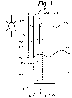
region 105, for example as illustrated in Figure 4.
[17] Figure 4 is a section view through section line A-A of Figure 1,
according to
some embodiments. With reference to Figure 4, first seal member 151 may
CA 02720257 2010-09-30
WO 2009/126170 PCT/US2008/069175
-5-
be affixed to opposing peripheral regions 105 of inner major surfaces 122 of
substrates 11, 12, in order to join substrates 11, 12 to one another, leaving
an
outer perimeter channel between the outer portions of the opposing peripheral
regions 105 to be.later filled with second seal member 1.52: First seal
member 151 is preferably formed from a polymer material, which has low
moisture vapor transmission properties, for example, any of those referenced
above; and second seal member 152 may be formed of any material having
suitable adhesive properties, for example, silicone, polysulfide or
polyurethane.
[18] According to some preferred embodiments, first substrate 11 is light
transmitting, for example, formed from glass or a plastic material, such as
polycarbonate, and second substrate 12 may be similarly formed or may be
opaque. According to some alternate embodiments, second substrate is light
transmitting, for example, formed from glass or a plastic material, such as
polycarbonate, and first substrate 11 may be similarly formed or may be
opaque. Although the term "glazing" typically connotes incorporation of a
glass panel or substrate, the use of the term is not so limited in the present
disclosure, and glazing assemblies of the present invention may incorporate
any light transmitting substrate, for example, formed from a plastic such as
polycarbonate. Figure 4 further illustrates glazing assembly 10 including a
photovoltaic coating 400 extending over, and being adhered to, inner major
surface 122 of first substrate 11, and a flexible and electrically non-
conductive
film 450 extending over photovoltaic coating 400, such that coating 400 is
sandwiched between substrate 11 and film 450, and airspace 200 is located
between an exposed surface 45 of film and second substrate 12.
[19] Film 450 may be formed, preferably pre-formed prior to application over
coating 400, from a polyolefin material, for example, a polyethylene or
polypropylene, or from a polyester material, and may have a thickness
between approximately 0.001 inch and approximately 0.015 inch, preferably
approximately 0.0035 inch. According to some preferred embodiments, film
450, when pre-formed, includes an adhesive backing 421 for adhering film
CA 02720257 2010-09-30
WO 2009/126170 PCT/US2008/069175
-6-
450 to coating 400, and may be supplied in rolls. Adhesive backing 421 may
be formed by an acrylic adhesive or by a rubber-based adhesive, or by any
other suitable adhesive known to those skilled in the art, and may extend over
approximately an entirety of the interface between:film 450 and coating 400 or
just over selected portions of the interface. Alternatively, film 450 may be
otherwise secured over coating 400, for example, a perimeter of film 450 may
be captured between a portion of seal system 15 and first substrate.
[20] According to embodiments of the present invention, substrate 11,
photovoltaic
coating 400 and flexible and electrically non-conductive film 450 form a
photovoltaic panel of assembly 10 so that assembly *10 can function as a solar
power cell. Photovoltaic coating 400 may be of any type known to those
skilled in the art, either of the conventional type, for example, including an
array of silicon wafers interconnected by soldered conductors, or of the `thin
film' type, for example, including several thin film semiconductor layers,
which
are patterned to form electrically interconnected cells. An embodiment of the
present invention, which includes coating 400 as a thin film CdTe type is
described in conjunction with Figure 5, however, it should be appreciated that
alternate embodiments may incorporate coating 400 as a thin film
Cu(InGa)Se2 (CIGS) type or amorphous silicon(a-Si) type.
[21] Because film 450 is enclosed between first and second substrates 11, 12
of
glazing assembly 10, film 450 need not have a durability that is otherwise
required for exposed polymer back skins employed by some photovoltaic
panels known in the art. However, according to some preferred
embodiments, film 450 has properties such that the integrity of film 450 is
maintained under thermal cycling conditions, for example, temperatures
ranging between approximately - 40 C and approximately 85 C, over a life
span of up to, and preferably exceeding, approximately 20 years.
[22] With further reference to Figure 4, a dotted line schematically
represents an
optional desiccant material enclosed within airspace 200 to absorb any
moisture that may pass through seal system 15. The desiccant material,
either in sheet or strip form, or granular form, either embedded in a matrix
or
CA 02720257 2010-09-30
WO 2009/126170 PCT/US2008/069175
-7-
packaged in a sack, may be `free-floating' in airspace 200,. or adhered to
exposed surface 45 of film 450 or to second substrate 12, or otherwise
present in airspace 200. The desiccant material, in combination with the
aforementioned relatively low MVTR of seal system 15, may prevent moisture
build-up within airspace 200 that can lead to corrosion of certain elements of
photovoltaic coating 400. According to some embodiments, a plurality of
desiccant beads are adhered to a surface of a sheet-like material, or tape,
which is then adhered to exposed surface 45 of film 450.
[23] Figure 5 is a cross-section of the photovoltaic panel portion of the
assembly
shown in Figure'4, according to one embodiment. Figure 5 illustrates coating
400 including a first layer 401 formed by a transparent conductive oxide
(TCO), for example, comprising Tin oxide (Sn02), which is overlaid with a
semiconductor layer 402, for example, comprising two `sub-layers': Cadmium
sulfide (CdS; `window' layer; n-type), extending adjacent to first layer 401,
and
Cadmium Telluride (CdTe; absorbing layer; p-type), overlaying the Cadmium
sulfide sub-layer. Figure 5 further illustrates an electrical contact layer
403,
for example, comprising nickel, which extends between the Cadmium
Telluride sub-layer of semiconductor layer 402, and a pair of bus bars 404A,
404B. Bus bars 404A, 404B may each be formed from a copper tape, for
example, approximately 0.003 - 0.007 inch thick, which are adhered to contact
layer 403, for example, by a conductive acrylic adhesive. Bus bars 404A,
404B preferably extend approximately parallel to one another along opposing
edge portions of coating 400; an internal insulated conductor 407 is coupled
to each bus bar 404A, 404B, and conductors 407 terminate near an electrical
access opening 480 in film 450 (Figure 3). Film 450 can provide additional
retention for holding bus bars 404A, 404B in intimate contact with contact
layer 403 and for securing insulated conductors 407 against layer 400. An
electrical lead 420, which is shown in Figures 1, 3 and 4, includes a pair of
isolated conductive lead wires to collect power from the photovoltaic panel;
each lead wire is coupled to a corresponding conductor 407, for example, via
soldering to a respective terminal thereof in proximity to opening 480.
CA 02720257 2010-09-30
WO 2009/126170 PCT/US2008/069175
-8-
[24] With reference to Figure 1, second substrate12 is shown including an
opening
18, which is approximately aligned with electrical access opening 480, and
extends through second substrate 12, to allow further passage of lead 420 out
from assembly 10. A diameter of openings 480, 18 may be between
approximately 1/4 inch and approximately 1 inch. According to the illustrated
embodiment, after routing lead 420 out from system 10, through opening 18, a
potting material. is applied around lead 420, to seal off opening 18. Examples
of suitable potting materials include, without limitation, polyurethane,
epoxy,
polyisobutylene, and any low MVTR material. According to alternate
embodiments, one "or both of openings 480, 18 are not necessary and lead
420 extends out from assembly 10 through an opening in seal system 15 or
through an opening between seal system 15 and one of substrates 11, 12, or
through an opening in first substrate 11.
[25] According to some preferred embodiments of the present invention, the
flexibility of film 450, in combination with a tear strength thereof, is
suited to
hold substrate 11 and photovoltaic coating 400 together in case substrate 11
is fractured, thereby containing fragments of the fractured substrate 11 to
prevent a scattering of potentially toxic elements of photovoltaic coating
400,
for example, Cadmium. Furthermore, in the event that substrate 12 is broken,
the electrical insulating properties of film 450 preferably electrically
isolates
coating 400 and electrically charged conductors 407, which are coupled to
bus bars 404A,B of coating 400, thereby preventing potential injury to one
handling the broken assembly. Film 450 may further protect the
semiconductor sub-layers of coating 400 if, during relatively cold temperature
conditions, the air space between substrates 11, 12 shrinks such that
substrates 11, 12 come into contact. According to some embodiments, in
which sun light is received by coating 400 through first substrate 11, for
example, in the case of the CdTe type of coating (Figure 5), and second
substrate 12 is translucent or transparent, flexible film 450 is opaque to
provide a more aesthetically pleasing uniform appearance to the photovoltaic
panel, when viewed through second substrate 12. According to those
CA 02720257 2010-09-30
WO 2009/126170 PCT/US2008/069175
-9-
embodiments in which coating 400 is the CIGS type, since sun light is
received by the coating 400 through second substrate 12 and through film
450, film 450 needs to light transmitting.
[26] Figure 6 is a flowchart outlining some assembly methods.of'.the present
invention, which start with a first substrate, for example, first substrate
11, that
has a photovoltaic coating, for example, coating 400 (Figure 4), already
formed over a central region of a major surface thereof, for example, central
region 103 of surface 122 (Figure 2). This pre-formed photovoltaic coating
preferably extends over the central region of the major surface of the first
substrate, without significantly encroaching on a peripheral region of the
surface, for example, region 105 (Figures 2 and 5), so as to maintain
exposure of a native surface of the substrate for fixation to a sealing
member,
for example, included in sealing system 15, which joins the first substrate to
an opposing second substrate, for example, second substrate 12. According
to the outlined method, an opening is formed in a sheet of flexible and
electrically non-conductive film, for example, electrical access opening 480
in
film 450 (Figure 3), per step 601, and then the photovoltaic coating of the
first
substrate is overlaid with the film, per step 603. As previously described,
the
film is adhered to the photovoltaic coating, preferably by means of an
adhesive backing pre-formed on a surface of the film. The overlaid film
preferably covers an entirety of the photovoltaic coating, for example, as
shown in Figure 5, while leaving enough of the peripheral region of the
surface of the first substrate, for example region 105, free for fixation with
a
sealing member that will join the first substrate to the second substrate.
However, according to some embodiments, the film may not cover a portion of
a perimeter of the coating, which portion may extend between the sealing
member and the first substrate.
[27] According to the outlined method, following step 603, the seal member is
applied to one of first and second substrates, per step 605, and then second
substrate is joined to first substrate, per step 615. Joining the first
substrate
to the second substrate, per step 615, includes pressing the two substrates
CA 02720257 2010-09-30
WO 2009/126170 PCT/US2008/069175
-10-
together, with the seal member sandwiched therebetween along the
peripheral regions of the facing major surfaces, while maintaining an air
space, for example air space 200 (Figure 4), between the central regions of
the facing major surfaces; heat may be applied, along with. pressure, to
securely affix the seal member to each of the substrates. Prior to joining the
second substrate to the first substrate, per step 615, an opening, for
example,
opening 18 (Figure 1), is formed in second substrate, per step 610, according
to the outlined method. The opening in the second substrate is preferably
aligned with the opening in the film when the second substrate is joined to
the
first substrate, per step 615.
[28] After joining the second substrate to the first substrate, an external
lead, for
example, lead 420 (Figures 1, 3 and 4), is coupled, through the openings in
the film and the second substrate, to internal conductors, for example,
conductors 407 (Figure 5), which extend from the bus bars of the photovoltaic
coating, per step 617, as previously described. According to step 619, a
potting material is applied around the lead at the opening to seal of the
opening, also as previously described; the potting material may further form a
strain relief for the lead adjacent to the second substrate, or a separate
strain
relief member may be installed about the lead. Finally, if the aforementioned
seal member, which joins the first substrate to the second substrate, is a
first
of a pair of seal members in a seal system, for example, seal system 15
illustrated in Figure 4, the second seal member, for example, seal member
152, is applied about a perimeter of the first seal member in between the
first
and second substrates, per optional step 620.
[29] In the foregoing detailed description, the invention has been described
with
reference to specific embodiments. However, it may be appreciated that
various modifications and changes can be made without departing from the
scope of the invention.