Note: Descriptions are shown in the official language in which they were submitted.
CA 02720966 2010-10-07
WO 2009/137286 PCT/US2009/041780
3-D INTEGRATED CIRCUIT LATERAL HEAT DISSIPATION
FIELD OF DISCLOSURE
[0001] This disclosure relates to integrated circuits (ICs), and
more
specifically to multi-tiered (3-D) ICs, and even more specifically to systems
and
methods for enhancing heat dissipation in 3-D ICs.
BACKGROUND
[0002] In IC technology there is a need to stack the chips (dies)
together
to form multi-tiered or three-dimensional (3-D) IC devices. One result of such
3-D IC
stacking is a decrease of signal propagation time during signal processing,
due to the
reduced distance signals must travel when they remain within a single package.
[0003] One method for tier bonding is to bring two (or more) dies
together and then encapsulate the dies into a single structure. Electrical
conductors
and/or contacts on the surface of the respective dies serve to carry
electrical signals
between components on the different dies.
[0004] One problem when dies are positioned in close proximity to
each
other is that thermal density increases. Moreover, because of the reduced size
of
stacked ICs, (substrate thickness going from 700-100 microns to below 20
microns), the
lateral thermal conductivity is reduced. Thus, hot spots could exist with
little ability to
move the heat away from the heat source.
[0005] One method for increasing lateral thermal conductivity is
to
increase the substrate thickness of at least one of the tiers. Another method
is to
increase the metal layers in the chip to be able to dissipate heat This, in
turn, negatively
impacts the desired aspect ratio of the package, as well as degrades the
signal
transmission speeds.
[0006] An additional problem exists when more than one tier is
bonded.
In such situations, the stacked IC device contains multiple layers of oxide
between tiers.
Oxide, being a poor thermal conductor, adds to the heat dissipation problem.
[0007] There are several approaches that could be taken to help
with the
thermal conductivity issues. One such approach could use through-silicon-vias
(TSVs)
to move the heat from an inner portion to a surface layer, and then remove the
heat
using traditional methods, such as a high thermal conductivity material
positioned on a
surface of the IC package. A problem with such a solution is that a circuit
layout may
CA 02720966 2010-10-07
WO 2009/137286 PCT/US2009/041780
2
prevent positioning a TSV at the necessary location because of devices
constructed in
the various tiers in proximity to the hot spot generating the heat.
[0008] Another method is to circulate cooling material through the
stacked IC device to cool the various hot spots. This is costly to manufacture
because
the moving liquid requires a pumping mechanism and tight tolerances for liquid
channels. Also, it may not be possible to channel the cooling material to the
necessary
location. The channeling problem could be overcome, to some extent, by forcing
cooling liquid through the substrate itself, but this method is not without a
further set of
problems and costs.
SUMMARY OF THE DISCLOSURE
[0009] Embodiments of the invention fill an air gap between
stacked dies
with a thermally conductive material, which allows heat generated at one or
more
locations within each die to be laterally displaced. The lateral displacement
of the heat
can be along the full length of the die or along a portion of the length. In
one
embodiment, the thermal material is electrically insulating. In one
embodiment, TSVs,
perhaps using carbon nanotubes can be constructed at certain locations to
assist in heat
dissipation away from thermally troubled locations.
[0010] In one embodiment, a multi-tiered semi-conductor has a
thermally conductive material disposed between first and second tiers wherein
the
material has a higher thermal conductivity than the thermal conductivity of
said first and
second tiers.
[0011] In another embodiment, a method of manufacturing a tiered
semi-
conductor is disclosed in which a thermally conductive material is applied to
at least one
mating surface of a first die and the mating surface of that die is brought
into mated
contact with a mating surface of a second die.
[0012] In still another embodiment, a method for heat dissipation
in a
stacked IC device is disclosed which allows heat from a thermally troubled
area of one
layer of a multi-tiered IC device to flow to an inter-layer between adjacent
tiers of the
device, such that lateral heat flow is facilitated in the inter-layer area to
at least one heat
dissipation location in thermal communication with the inter-layer area. In
one
embodiment, the heat dissipation area is a via constructed through at least
one layer of a
tier of the device. In another embodiment, the heat dissipation area is a gap
between
adjacent dies in a same tier.
CA 02720966 2014-04-28
,
74769-3145
2a
10012a1 In one aspect, there is provided a three dimensional
integrated circuit (IC)
device, comprising: a first die stacked on a second die, each die comprising
an active face and
a substrate, the dies' active faces coupled together by a plurality of tier to
tier connections,
and the tier to tier connections creating a gap between the active faces of
the first and second
die; a through-substrate via filled with a first thermally conductive material
disposed in the
first die; and a thermally conductive layer positioned within the gap.
10012131 In another aspect, there is provided a three dimensional
integrated circuit (IC)
device, comprising: a first die and a second die, each die comprising an
active face and a
substrate; means for coupling the dies' active faces, the means for coupling
creating a gap
between the first die and second die; means, disposed in a via extending
through the first die,
for conducting heat; and means disposed within the gap, for conducting heat.
[0012c] In another aspect, there is provided a three dimensional
integrated circuit (IC)
device, comprising: a first die stacked on a second die, the first die being
circumferentially
larger than the second die; the first and second dies coupled together by a
plurality of tier to
tier connections, and the tier to tier connections creating a gap between the
first and second
die; a through-substrate via filled with a thermally conductive material
disposed in the first
die; and the second die comprising a thermally conductive layer.
[0012d] In another aspect, there is provided an integrated circuit
(IC) device,
comprising: a first die comprising an active layer on a substrate, a through-
substrate via filled
with a thermally conductive material disposed in the first die; and a
thermally conductive and
electrically insulating layer directly coupled to only the active layer of the
first die distal from
the substrate.
[0012e] In another aspect, there is provided a method for heat
dissipation in a multi-
tiered three dimensional integrated circuit (IC) device, said method
comprising: allowing heat
from a thermally troubled area of one tier of the IC device to flow to an
inter-layer area
between adjacent tiers of said device; and facilitating heat flow laterally in
said inter-layer
area to at least one heat dissipation location in thermal communication with
said inter-layer
area, wherein said at least one heat dissipation location comprises a via
constructed through a
CA 02720966 2014-04-28
74769-3145
2b
portion of at least one tier of said device, the via being laterally displaced
from the thermally
troubled area.
[0012f1 In another aspect, there is provided a three dimensional
integrated circuit, IC,
device, comprising: a first die stacked on a second die creating a first gap
between the first
and second dies, the dies having elements constructed therein; a first
thermally conductive
material disposed in the first gap created between the first and second dies
wherein the first
thermally conductive material has a higher thermal conductivity than a thermal
conductivity
of the first and second dies; and a first thermally conductive via being
thermally coupled to
the first thermally conductive material and positioned through at least a
portion of a layer of
the first die at a location laterally displaced from a thermally troubled area
within the IC
device.
CA 02720966 2013-07-11
74769-3145
3
[0013] The foregoing has outlined rather broadly the features and
technical advantages
of the present invention in order that the detailed description that follows
may be better
understood. Additional features and advantages will be described hereinafter
which form the
subject of the claims of the invention. It should be appreciated by those
skilled in the art that
the conception and specific embodiments disclosed may be readily utilized as a
basis for
modifying or designing other structures for carrying out the same purposes of
the present
invention. It should also be realized by those skilled in the art that such
equivalent
constructions do not depart from the scope of the invention as set forth in
the appended
claims. The novel features which are believed to be characteristic of the
invention, both as to
its organization and method of operation, together with further objects and
advantages will be
better understood from the following description when considered in connection
with the
accompanying figures. It is to be expressly understood, however, that each of
the figures is
provided for the purpose of illustration and description only and is not
intended as a definition
of the limits of the present invention.
BRIEF DESCRIPTION OF THE DRAWINGS
[0014] For a more complete understanding of the present disclosure,
reference is now
made to the following descriptions taken in conjunction with the accompanying
drawings.
[0015] FIGURE 1 is a cross sectional side view illustrating one
aspect of thermal
trouble conditions that could exist with 3-D integrated circuits.
[0016] FIGURE 2 is a cross sectional side view illustrating one exemplary
solution to
the heat removal problem.
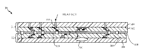
[0017] FIGURE 3 is a cross sectional side view showing one
embodiment of the
concepts of the disclosure.
[0018] FIGURE 4 shows one embodiment of method for constructing
stacked IC
device in accordance with the teaching of the disclosure.
CA 02720966 2013-07-11
74769-3145
3a
DESCRIPTION OF THE EMBODIMENTS OF THE INVENTION
100191
FIGURE 1 illustrates one aspect of thermal trouble conditions that could exist
with 3-D integrated circuits. As shown in FIGURE 1, a die 11 is stacked with a
die 12. The
active layer of die 11 is a layer 102 and the active layer of
CA 02720966 2010-10-07
WO 2009/137286 PCT/US2009/041780
4
die 12 is a layer 103. This is an exemplary arrangement as the active layers
of the dies
could be in any orientation, up or down.
[0020] Vias 105 run through the substrate layer 101 of the die 11.
Vias
could be constructed in the layers 102, 103 and/or 104 as desired. Electrical
paths 107
and 108 form an interconnect between the dies. Seal 109 acts to prevent non-
desired
contaminants from entering the area 120 between the respective dies 11, 12..
[0021] Element 108 is normally on the scale of 30 microns or less
and
normally forms a copper or a tin copper metal to metal bond. Area 120 is
usually an air
gap. The gap 120 can be in the range of less than 10 micron.
[0022] A hot spot 110 is on the die 12 and the challenge is to
move heat
from this relatively small area 110 to an external portion of the die stack.
Note that
elements 111 are directly above the hot spot 110 and would be affected by heat
from the
hot spot 110 moving upward through the layers 103, 102, 101.
[0023] FIGURE 2 illustrates one discussed solution to the heat
removal
problem. In this solution, a TSV array 200 having individual TSVs 201, 202,
and 203 is
positioned to provide thermal conductivity for heat from the hot spot 110. The
heat
passes through the layer 103, which is the active area of bottom die 12. The
heat then
passes through the active layer 102 of the die 11 and is then pulled out to
the exterior
via the TSV array 200. The vias 201, 202, 203 may be copper or tungsten lined
to
increase thermal conductivity, but any thermally conductive material would
work. In
one embodiment, carbon nanotubes (CNTs) can be used to fill the vias 201, 202,
203.
In another embodiment, CNTs partially fill the vias 201, 202, 203 and metal
fills the
remainder of the vias 201, 202, 203. An advantage of the CNTs is improved
electrical
and thermal conductivity, as well as improved current density.
[0024] FIGURE 3 shows one embodiment 30 in which the concepts of
the disclosure are utilized. Thermally conductive material 320 is positioned
within a
gap between the dies 31 and 32. In another embodiment, the thermally
conductive
material 320 is between metal layers (not shown) of one of the active layers
302, 303 of
the tiers 31, 32. The thermally conductive material 320 ideally would have
thermal
conductivity greater than 10 W/m/K so as to facilitate lateral heat transfer.
The material
320 is thermally conductive, and in one embodiment electrically insulating so
that it
does not short circuit the electrical connections that connect the dies 31,
32, which
would interfere with the operation of elements contained in the dies 31, 32.
The
CA 02720966 2010-10-07
WO 2009/137286 PCT/US2009/041780
material 320 can be positioned by a variety of methods, for example, spun on
or
deposited by chemical vapor deposition (CVD), and/ or physical vapor
deposition
(PVD). The material 320 may be a diamond matrix or a diamond film pattern.
[0025] Although only shown on one layer 302 of one of the dies 31,
the
material 320 can be positioned on a surface of each of the two mating layers
302, 303,
so that the material 320 on each layer 302, 303 actually touches each other
when the
dies 31, 32 are stacked. Alternatively, the material 320 may be placed only on
one of
the mating layers 302, 303.
[0026] In operation, heat from hot spot 310 passes upward through
the
layer 303 of the die 32 and into the material 320. The heat then travels
laterally along
the material 320 either to an edge of the device, such as over hanging edge
330 or more
typically, the heat will pass up through one or more heat dissipating vias,
such as
through the via 331 constructed in the layer 301 of the die 31. Because of the
lateral
movement of the heat, there is a better uniformity of the temperature across
the device
30. This benefit allows heat to spread relatively quickly across the whole
device 30,
thereby causing the device 30 to evenly heat up. The removal of heat from a
larger area,
such as the entire device 30 or the package of the device is easier to
accomplish than
removing heat from a small, internal area.
[0027] Note that the heat dissipating via 331 can pass up through
die 31,
or down through die 32 (or both). One advantage of the thermally conductive
material
320 is that the heat dissipating via 331 can be laterally offset from the
thermally
troubled area 310 thereby freeing areas directly above the troubled area to be
used for
circuitry or other elements constructed in the various layers 301, 302, 303.
Also note
that the heat need not flow directly upward through the layers 301, 302, 303
but rather
the via 331 could, for example, be angled and/or curved. Another advantage of
the
lateral heat dissipation is that fewer TSVs are needed.
[0028] For multi-tiered devices having more than two tiers,
multiple
inter-layer heat dissipating material structures can be used. Thus, the heat
can move
laterally from the heat source a first distance within a first inter-layer
area and then pass
up one tier with the assistance of a via and then again move laterally (in any
direction)
in a second inter-layer area, provided thermally conductive material is
positioned in
both first and second inter-layer areas.
CA 02720966 2013-07-11
=
74769-3145
6
[0029] One system for allowing even greater heat removal from the
material 320 is to
make one of the layers, such as the dies 31 circumferentially larger than the
other die 32
thereby creating a surface area, such as surface area 330 on an overhanging
lip on the larger of
the dies. Note that this same technique would work for several tiers which, if
desired, could
be staggered as to diameter. The composition of the material 320 need not be
the same across
the entire surface and the differences in the material 320 could be used to
assist in heat
conductivity away from the hot spot(s) 310.
[0030] In one embodiment, a bottom die is larger than a top die.
Thus, a gap would
exist between two top dies (of a single tier) that rest on the bottom die.
According to the
present disclosure, gap fill material can be provided within this gap between
the top dies. The
gap fill material can be thermally conductive and can be any material with
good thermal
conductivity, such as a diamond film. In one embodiment, the thermally
conductive gap fill
material is thermally coupled to the material 320 to help transfer heat out of
the stacked IC
device.
[0031] FIGURE 4 shows one embodiment 40 of a method for constructing
stacked IC
devices in accordance with the teachings of the disclosure. Process 401
determines if a die
has been selected for constructing a stacked IC device. If not, then process
402 controls a
wait time. After a die has been selected, process 403 determines if a
thermally conductive
material should be added to at least one lateral surface of the die. The
thermally conductive
material can be deposited under control of process 404 by any one of the
methods discussed
above, such as CVD or PVD processing, or the material can be spun on, or
applied as a film.
[0032] Processes 405 and 406 wait for a next die to be selected for
mating with the
previously selected die. Process 407 and 408 add thermally conductive material
to this next
die, if appropriate, and process 409 then bonds the dies together. Process 410
determines if
more dies are to be added. When all the dies have been selected and coated
with thermally
conductive material (if appropriate), process 411 completes the IC package
which is then
available for testing and/or usage.
[0033] Although the present invention and its advantages have been
described in
detail, it should be understood that various changes, substitutions and
alterations can be made
CA 02720966 2013-07-11
74769-3145
6a
herein without departing from the scope of the invention as defined by the
appended claims.
For example, although the material 320 has been described as being non-
electrically
conductive, it is possible to make the
CA 02720966 2010-10-07
WO 2009/137286 PCT/US2009/041780
7
material electrically conductive. In this embodiment, the electrically
conductive
material should be patternable, i.e., capable of being patterned, such that it
can be
separated from some vias to prevent electrical connections while still
thermally
dissipating heat.
[0034] The scope of the present application is not intended to be
limited
to the particular embodiments of the process, machine, manufacture,
composition of
matter, means, methods and steps described in the specification. As one of
ordinary
skill in the art will readily appreciate from the disclosure, processes,
machines,
manufacture, compositions of matter, means, methods, or steps, presently
existing or
later to be developed, that perform substantially the same function or achieve
substantially the same result as the corresponding embodiments described
herein, may
be utilized according to the present invention. Accordingly, the appended
claims are
intended to include within their scope such processes, machines, manufacture,
compositions of matter, means, methods, or steps.