Note: Descriptions are shown in the official language in which they were submitted.
CA 02721671 2010-10-15
DESCRIPTION
TITLE OF THE INVENTION
Semiconductor Device
TECHNICAL FIELD
The present invention relates to a semiconductor device and a method of
manufacturing the same, and more particularly to a semiconductor device
including an
electrode arranged in contact with an SiC wafer composed of silicon carbide.
BACKGROUND ART
In a semiconductor device, in many cases, a structure in which an n-type
region
having an n conductivity type and a p-type region having a p conductivity type
are
formed and an electrode is connected to the n-type region and the p-type
region is
adopted. With higher efficiency being achieved in recent years in an apparatus
where a
semiconductor device is included, a semiconductor device is also required to
achieve
higher efficiency. In order to achieve higher efficiency of a semiconductor
device, the
electrode above should be low not only in its own resistance (electrical
resistance) but
also in contact resistance with the n-type region and the p-type region above.
Meanwhile, in order to achieve a higher withstand voltage and lower loss of a
semiconductor device and to enable use thereof in an environment at a high
temperature,
silicon carbide (SiC) has recently been adopted as a material for forming a
semiconductor device. SiC is a wide-bandgap semiconductor greater in bandgap
than
silicon (Si) that has conventionally widely been used as a material for
forming a
semiconductor device. Therefore, by adopting SiC as a material for forming a
semiconductor device, a higher withstand voltage, a lower ON resistance and
the like of
a semiconductor device can be achieved. In addition, a semiconductor device
adopting
SiC as a material is also advantageous in that lowering in characteristics
when used in an
environment at a high temperature is less likely than in a semiconductor
device adopting
Si as a material.
-1-
CA 02721671 2010-10-15
In adopting SiC as a material for a semiconductor device, however, it is
difficult
to avoid increase in Schottky barrier between a p-type region, an n-type
region and an
electrode as compared with an example where Si is adopted as a material for a
semiconductor device. Consequently, a problem of difficulty in suppression of
increase
in contact resistance between a p-type region, an n-type region and an
electrode has
arisen.
In contrast, it has been known that contact resistance can be lowered by
adopting Ni (nickel) as a material for an electrode in contact with an n-type
SiC region
containing an n-type impurity (an impurity having an n conductivity type) and
adopting
Ti (titanium)/Al (aluminum) or AISi alloy as a material for an electrode in
contact with a
p-type SiC region containing a p-type impurity (an impurity having a p
conductivity
type) (see, for example, Satoshi TANIMOTO et al., "Practical Device-Directed
Ohmic
Contacts on 4H-SIC," IEICE Transactions C, the Institute of Electronics,
Information
and Communication Engineers, April 2003, Vol. J86-C, No. 4, pp. 359-367 (Non-
Patent
Document 1)).
PRIOR ART DOCUMENTS
NON-PATENT DOCUMENTS
Non-Patent Document I : Satoshi TANIMOTO et al., "Practical Device-Directed
Ohmic Contacts on 4H-SiC," IEICE Transactions C, the Institute of Electronics,
Information and Communication Engineers, April 2003, Vol. J86-C, No. 4, pp.
359-367
SUMMARY OF THE INVENTION
PROBLEMS TO BE SOLVED BY THE INVENTION
As described above, by appropriately selecting a material for forming an
electrode in accordance with whether a region in contact with an electrode is
an n-type
SiC region or a p-type SiC region, contact resistance between a p-type region,
an n-type
region and an electrode can be lowered even when SiC is adopted as a material
for a
semiconductor device. If a material for forming an electrode in contact with
the p-type
region is different from a material for forming an electrode in contact with
the n-type
-2-
CA 02721671 2010-10-15
region, however, a plurality of steps for forming these electrodes are
required, which
leads to increase in the number of steps in a manufacturing process.
Consequently, a
problem of increase in manufacturing cost of a semiconductor device arises. In
addition, difference between a material for forming an electrode in contact
with the p-
type region and a material for forming an electrode in contact with the n-type
region
may prevent improvement in integration of a semiconductor device.
From the foregoing, an object of the present invention is to provide a
semiconductor device capable of achieving decrease in the number of steps in a
manufacturing process and improvement in integration by including an electrode
that
can be in contact with any of a p-type SiC region and an n-type SiC region
with contact
resistance being sufficiently suppressed.
MEANS FOR SOLVING THE PROBLEMS
A semiconductor device according to one aspect of the present invention
includes an SiC wafer composed of silicon carbide and an ohmic contact
electrode
arranged in contact with the SiC wafer and containing titanium, aluminum,
silicon, and
carbon as well as a remaining inevitable impurity. The SiC wafer includes an n-
type
region having an n conductivity type and a p-type region having a p
conductivity type.
In addition, each of the n-type region and the p-type region is in contact
with the ohmic
contact electrode above. The ohmic contact electrode contains aluminum and
titanium
in a region including an interface with the SiC wafer.
An ohmic contact electrode constituting a semiconductor device according to
one aspect of the present invention contains aluminum and titanium in a region
including
an interface with the SiC wafer. Thus, the ohmic contact electrode can be in
contact
with any of the p-type SiC region and the n-type SiC region with contact
resistance
being sufficiently suppressed. Consequently, according to the semiconductor
device in
one aspect of the present invention, an ohmic contact electrode in contact
with the p-
type region and an ohmic contact electrode in contact with the n-type region
can be
made of the same material, and a semiconductor device capable of achieving
decrease in
-3-
CA 02721671 2010-10-15
the number of steps in a manufacturing process and improvement in integration
can be
provided. Here, a state that "aluminum and titanium are contained in a region
including an interface with an SiC wafer" refers to such a state that presence
of
aluminum and titanium in a region including an interface with an SiC wafer can
be
detected to an extent clearly distinguishable from noise, for example, by
conducting
Auger spectroscopic analysis.
In the semiconductor device in one aspect above, the ohmic contact electrode
above may be arranged to extend from a region in contact with the n-type
region to a
region in contact with the p-type region.
In addition, the semiconductor device in one aspect above may include a
plurality of ohmic contact electrodes, one ohmic contact electrode of the
plurality of
ohmic contact electrodes may be in contact with the n-type region, and another
ohmic
contact electrode may be in contact with the p-type region.
A semiconductor device according to another aspect of the present invention
includes an SiC wafer composed of silicon carbide and an ohmic contact
electrode
arranged in contact with the SiC wafer and containing titanium, aluminum,
silicon, and
carbon as well as a remaining inevitable impurity. The SiC wafer includes an n-
type
region having an n conductivity type and a p-type region having a p
conductivity type.
In addition, each of the n-type region and the p-type region is in contact
with the ohmic
contact electrode above. A region of the ohmic contact electrode including a
surface
opposite to the SiC wafer contains silicon.
An ohmic contact electrode constituting a semiconductor device according to
another aspect of the present invention contains silicon in a region including
a surface
opposite to the SiC wafer. Thus, by containing silicon (Si) in the region
including the
surface opposite to the SiC wafer, the ohmic contact electrode can be in
contact with
any of the p-type SiC region and the n-type SiC region with contact resistance
being
sufficiently suppressed. Consequently, according to the semiconductor device
in
another aspect of the present invention, an ohmic contact electrode in contact
with the
-4-
CA 02721671 2010-10-15
p-type region and an ohmic contact electrode in contact with the n-type region
can be
made of the same material, and a semiconductor device capable of achieving
decrease in
the number of steps in a manufacturing process and improvement in integration
can be
provided. Here, a state that "a region including a surface opposite to an SiC
wafer
contains silicon" refers to such a state that presence of silicon in a region
including a
surface opposite to an SiC wafer can be detected to an extent clearly
distinguishable
from noise, for example, by conducting Auger spectroscopic analysis.
In the semiconductor device in another aspect above, a content of silicon in
the
ohmic contact electrode may monotonously increase toward the SiC wafer.
In addition, in the semiconductor device in another aspect above, a content of
aluminum in the ohmic contact electrode may monotonously decrease toward the
SiC
wafer.
In addition, in the semiconductor device in another aspect above, a content of
titanium in the ohmic contact electrode may monotonously increase from the
surface
opposite to the SiC wafer toward the SiC wafer and attain to a maximum value,
and
thereafter may monotonously decrease.
In addition, in the semiconductor device in another aspect above, the ohmic
contact electrode may be arranged to extend from a region in contact with the
n-type
region to a region in contact with the p-type region.
In addition, the semiconductor device in another aspect above may include a
plurality of ohmic contact electrodes, one ohmic contact electrode of the
plurality of
ohmic contact electrodes may be in contact with the n-type region, and another
ohmic
contact electrode may be in contact with the p-type region.
A semiconductor device according to yet another aspect of the present
invention
includes an SiC wafer composed of silicon carbide and an ohmic contact
electrode
arranged in contact with the SiC wafer and containing titanium, aluminum,
silicon, and
carbon as well as a remaining inevitable impurity. The SiC wafer includes an n-
type
region having an n conductivity type and a p-type region having a p
conductivity type.
-5-
CA 02721671 2010-10-15
In addition, each of the n-type region and the p-type region is in contact
with the ohmic
contact electrode above. In the ohmic contact electrode, a content of aluminum
monotonously decreases toward the SiC wafer and a content of silicon
monotonously
increases toward the SiC wafer.
In the ohmic contact electrode constituting the semiconductor device according
to yet another aspect of the present invention, a content of aluminum
monotonously
decreases toward the SiC wafer and a content of silicon monotonously increases
toward
the SiC wafer. Thus, the ohmic contact electrode can be in contact with any of
the p-
type SiC region and the n-type SiC region with contact resistance being
sufficiently
suppressed. Consequently, according to the semiconductor device in yet another
aspect of the present invention, an ohmic contact electrode in contact with
the p-type
region and an ohmic contact electrode in contact with the n-type region can be
made of
the same material, and a semiconductor device capable of achieving decrease in
the
number of steps in a manufacturing process and improvement in integration can
be
provided.
In the semiconductor device in yet another aspect above, a content of titanium
in
the ohmic contact electrode may monotonously increase from a surface opposite
to the
SiC wafer toward the SiC wafer and attain to a maximum value, and thereafter
may
monotonously decrease.
In addition, in the semiconductor device in yet another aspect above, the
ohmic
contact electrode may be arranged to extend from a region in contact with the
n-type
region to a region in contact with the p-type region.
In addition, the semiconductor device in yet another aspect above may include
a
plurality of ohmic contact electrodes, one ohmic contact electrode of the
plurality of
ohmic contact electrodes may be in contact with the n-type region, and another
ohmic
contact electrode may be in contact with the p-type region.
A state that a content of an element monotonously increases or decreases
refers
to a state that an ohmic contact electrode does not have a region where a
content of an
-6-
CA 02721671 2010-10-15
element is constant (for example, a continuous region where the content is 0)
in a
direction of thickness thereof and the content continues to increase or
decrease.
EFFECTS OF THE INVENTION
As can clearly be understood from the description above, according to the
semiconductor device of the present invention, a semiconductor device capable
of
achieving decrease in the number of steps in a manufacturing process and
improvement
in integration by including an electrode that can be in contact with any of a
p-type SiC
region and an n-type SiC region with contact resistance being sufficiently
suppressed can
be provided.
BRIEF DESCRIPTION OF THE DRAWINGS
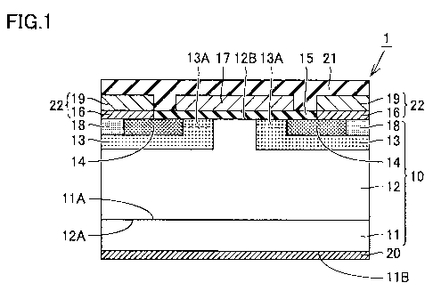
Fig. 1 is a schematic cross-sectional view showing a structure of a MOSFET.
Fig. 2 is a flowchart showing outlines of a method of manufacturing a MOSFET.
Fig. 3 is a flowchart showing details of an ohmic electrode formation step and
a
drain electrode formation step in Fig. 2.
Fig. 4 is a schematic cross-sectional view for illustrating a method of
manufacturing a MOSFET.
Fig. 5 is a schematic cross-sectional view for illustrating the method of
manufacturing a MOSFET.
Fig. 6 is a schematic cross-sectional view for illustrating the method of
manufacturing a MOSFET.
Fig. 7 is a schematic cross-sectional view for illustrating the method of
manufacturing a MOSFET.
Fig. 8 is a schematic cross-sectional view for illustrating the method of
manufacturing a MOSFET.
Fig. 9 is a schematic cross-sectional view for illustrating the method of
manufacturing a MOSFET.
Fig. 10 is a schematic cross-sectional view showing a structure of a JFET.
Fig. 11 is a flowchart showing outlines of a method of manufacturing a JFET.
-7-
CA 02721671 2010-10-15
Fig. 12 is a schematic cross-sectional view for illustrating a method of
manufacturing a JFET.
Fig. 13 is a schematic cross-sectional view for illustrating the method of
manufacturing a JFET.
Fig. 14 is a schematic cross-sectional view for illustrating the method of
manufacturing a JFET.
Fig. 15 is a schematic cross-sectional view for illustrating the method of
manufacturing a JFET.
Fig. 16 is a schematic cross-sectional view for illustrating the method of
manufacturing a JFET.
Fig. 17 is a schematic cross-sectional view for illustrating the method of
manufacturing a JFET.
Fig. 18 is a diagram showing relation between a ratio of a film thickness of
an Al
film to a Ti film and contact resistivity.
Fig. 19 is a diagram showing relation between a film thickness of an Si film
and
contact resistivity.
Fig. 20 is an SEM photograph of a portion around an ohmic contact electrode in
an Example.
Fig. 21 is a diagram showing distribution of elements around the ohmic contact
electrode in Example.
Fig. 22 is a diagram showing distribution of elements around the ohmic contact
electrode in a Comparative Example.
MODES FOR CARRYING OUT THE INVENTION
An embodiment of the present invention will be described hereinafter with
reference to the drawings. In the drawings below, the same or corresponding
elements
have the same reference characters allotted and description thereof will not
be repeated.
(First Embodiment)
Initially, a MOSFET (Metal Oxide Semiconductor Field Effect Transistor) in the
-8-
CA 02721671 2010-10-15
first embodiment will be described. Referring to Fig. 1, a MOSFET 1 in the
first
embodiment includes an n+ SiC substrate 11 being a substrate composed of
silicon
carbide (SiC) and having an n conductivity type (a first conductivity type),
an n SiC
layer 12 serving as a semiconductor layer composed of SiC and having the n
conductivity type (the first conductivity type), a pair of p bodies 13 serving
as second-
conductivity-type regions having a p conductivity type (a second conductivity
type), an
n+ source region 14 serving as a high-concentration first-conductivity-type
region having
the n conductivity type (the first conductivity type), and a p+ region 18
serving as a high-
concentration second-conductivity-type region having the p conductivity type
(the
second conductivity). N- SiC layer 12 having p bodies 13, n+ source regions 14
and p+
regions 18 formed therein and n+ SiC substrate 11 constitute an SiC wafer 10
composed
of silicon carbide. N+ SiC substrate l 1 contains an n-type impurity (an
impurity having
the n conductivity type) such as N (nitrogen) at high concentration.
N- SiC layer 12 is formed on one main surface 11A of n+ SiC substrate 11, for
example, to a thickness of approximately 10 m, and it has the n conductivity
type by
containing an n-type impurity. Examples of n-type impurities contained in n
SiC layer
12 include N (nitrogen), and an impurity is contained at concentration lower
than
concentration of an n-type impurity contained in n+ SiC substrate 11, for
example, at
concentration of 5x10'1cm 3
A pair of p bodies 13 is formed such that the p bodies are separate from each
other so as to include a second main surface 12B which is a main surface
opposite to a
first main surface 12A which is a main surface on the n+ SiC substrate 11
side, and the
pair has the p conductivity type (the second conductivity type) by containing
a p-type
impurity (an impurity having the p conductivity type). For example, Al, B
(boron), or
the like is adopted as a p-type impurity to be contained in p body 13, and it
is contained
at concentration lower than concentration of the n-type impurity contained in
n+ SiC
substrate 11, for example, at concentration of 1 x 101 7cm 3.
N+ source region 14 is formed within each p body 13 so as to include second
-9-
CA 02721671 2010-10-15
main surface 12B and to be surrounded by p body 13. N` source region 14
contains an
n-type impurity such as P (phosphorus) at concentration higher than
concentration of
the n-type impurity contained in n SiC layer 12, for example, at concentration
of
1 x 1020cm 3.
P+ region 18 is formed to include second main surface 12B, on the side
opposite
to n+ source region 14 formed within the other p body 13, when viewed from n+
source
region 14 formed within one p body 13 of the pair of p bodies 13. P+ region 18
contains a p-type impurity such as Al or B at concentration higher than
concentration of
the p-type impurity contained in p body 13, for example, at concentration of I
x 1020cm3.
Referring further to Fig. 1, MOSFET 1 includes a gate oxide film 15 serving as
a
gate insulating film, a gate electrode 17, a pair of source contact electrodes
16, a source
interconnection 19, a drain electrode 20, and a passivation film 21.
Gate oxide film 15 is formed on second main surface 12B of n SiC layer 12 so
as to be in contact with second main surface 12B and to extend from an upper
surface of
one n+ source region 14 to an upper surface of the other n+ source region 14,
and it is
composed, for example, of silicon dioxide (SiO2).
Gate electrode 17 is arranged in contact with gate oxide film 15 so as to
extend
from one n+ source region 14 to the other n+ source region 14 over the same.
In
addition, gate electrode 17 is made of a conductor such as polysilicon, Al or
the like.
Source contact electrode 16 is arranged in contact with second main surface
12B,
so as to extend from a pair of n+ source regions 14, in a direction away from
gate oxide
film 15, to p+ region 18. Source contact electrode 16 contains titanium (Ti),
aluminum
(Al), silicon (Si), and carbon (C) as well as a remaining inevitable impurity.
Here, the
inevitable impurity includes oxygen (0) inevitably introduced during the
manufacturing
process. Source contact electrode 16 contains aluminum and titanium in a
region
including an interface with n SiC layer 12 where source region 14 and p+
region 18 are
formed.
Source interconnection 19 is formed in contact with source contact electrode
16
-10-
CA 02721671 2010-10-15
and it is made of a conductor such as Al. Source interconnection 19 is
electrically
connected to n+ source region 14 through source contact electrode 16. This
source
interconnection 19 and source contact electrode 16 constitute a source
electrode 22.
Drain electrode 20 is formed in contact with the other main surface 11B of n+
SiC substrate 11, which is a main surface opposite to one main surface 11A
which is a
main surface on a side where n SiC layer 12 is formed. For example, this drain
electrode 20 may be structured similarly to source contact electrode 16 above,
or it may
be made of another material capable of establishing ohmic contact with n+ SiC
substrate
11, such as Ni. Thus, drain electrode 20 is electrically connected to n+ SiC
substrate
11.
Passivation film 21 is formed to extend from one source interconnection 19
over
gate electrode 17 to the other source interconnection 19. This passivation
film 21 is
composed, for example, of Si02 and it has a function to electrically isolate
source
interconnection 19 and gate electrode 17 from outside and to protect MOSFET 1.
Namely, MOSFET 1 in the present embodiment includes SiC wafer 10 and
source contact electrode 16 serving as an ohmic contact electrode, that is
arranged in
contact with SiC wafer 10 and contains Ti, Al, Si, and C as well as a
remaining
inevitable impurity. SiC wafer 10 includes n+ source region 14 having the n
conductivity type and p+ region 18 having the p conductivity type. In
addition, each of
n+ source region 14 and p+ region 18 is in contact with source contact
electrode 16.
Source contact electrode 16 contains Al and Ti in the region including the
interface with
SiC wafer 10. Moreover, source contact electrode 16 is arranged to extend from
the
region in contact with n+ source region 14 to the region in contact with p+
region 18.
In general, in many cases, Ni is adopted as a material for an electrode in
contact
with the n-type SiC region. Meanwhile, in a DMOS-type vertical MOSFET
including,
for example, SiC as a material, a structure in which an electrode composed of
Ni is in
contact with both of a p-type SiC region and an n-type SiC region is adopted.
This is
because the DMOS-type vertical MOSFET requires an electrode in contact with
both of
-I1-
CA 02721671 2010-10-15
the p-type region and the n-type region, while an electrode composed of Ni can
be in
contact also with the p-type SiC region at contact resistivity around 10-2E29
cm2.
Though this contact resistivity of 10-2520cm2 indicates a numeric value
allowing use as
an ohmic contact electrode, it is not sufficiently low, taking into account
the fact that an
electrode composed of Ti/Al can be in contact with the p-type SiC region at
contact
resistivity around l0-3S2.cm2.
On the other hand, in an example where an electrode composed of Ti/Al is
adopted, though contact resistance with the p-type SiC region is sufficiently
suppressed,
contact resistivity with the n-type SiC region is around 10-352=cm2. This
contact
resistivity of 10-3).cm2 also indicates a numeric value allowing use as an
ohmic contact
electrode, however, contact resistance between the electrode composed of Ti/Al
and the
n-type SiC region is not sufficiently low, taking into account the fact that
an electrode
composed of Ni can be in contact with the n-type SiC region at contact
resistivity
around 10-6f2=cm2.
As a result of further study about a structure of an electrode in
consideration of
relation between such a structure of an electrode and contact resistance with
the p-type
SiC region and the n-type SiC region, the present inventor has found that
contact
resistance with any of the p-type SiC region and the n-type SiC region can
sufficiently be
suppressed by adopting an ohmic contact electrode containing Ti, Al, Si, and C
as well
as a remaining inevitable impurity and containing Al and Ti in a region
including an
interface with the p-type SiC region and the n-type SiC region.
Source contact electrode 16 constituting MOSFET 1 in the present embodiment
contains Ti, Al, Si, and C as well as a remaining inevitable impurity and
contains Al and
Ti in the region including the interface with n+ source region 14 and p+
region 18 formed
in SiC wafer 10. Thus, source contact electrode 16 can be in contact with any
of n+
source region 14 and p+ region 18 with contact resistance being sufficiently
suppressed.
Source contact electrode 16 is arranged to extend from the region in contact
with n+
source region 14 to the region in contact with p+ region 18. Consequently,
MOSFET 1
- 12-
CA 02721671 2010-10-15
in the present embodiment is a semiconductor device capable of achieving
decrease in
the number of steps in a manufacturing process and improvement in integration.
More specifically, in MOSFET I in the present embodiment having a DMOS
structure, it is necessary to hold n+ source region 14 and p body 13 at the
same potential.
Therefore, source contact electrode 16 is required to electrically be
connected to both of
n+ source region 14 and p body 13 with contact resistance being lowered. In
addition,
in MOSFET 1, in order to lower ON resistance, n+ source region 14 and source
contact
electrode 16 should electrically be connected to each other with contact
resistance being
suppressed. In order to meet such requirements and to achieve decrease in the
number
of steps in a manufacturing process and improvement in integration, source
contact
electrode 16 extending from the region in contact with n+ source region 14 to
the region
in contact with p body 13 with contact resistance being lowered is required.
In this
connection, source contact electrode 16 in MOSFET I in the present embodiment
is in
contact with both of n+ source region 14 and p+ region 18 (p body 13) at low
contact
resistance, by having the structure above. Consequently, MOSFET 1 is a
semiconductor device capable of achieving decrease in the number of steps in a
manufacturing process and improvement in integration while achieving higher
efficiency.
An operation of MOSFET 1 will now be described. Referring to Fig. 1, in such
a state that a voltage not higher than a threshold value is applied to gate
electrode 17,
that is, in an OFF state, a portion between p body 13 located directly under
gate oxide
film 15 and n SiC layer 12 is reverse-biased and in a non-conducting state. On
the
other hand, as a positively increasing voltage is applied to gate electrode
17, an
inversion layer is formed in a channel region 13 A, which is a region around a
portion of
contact of p body 13 with gate oxide film 15. Consequently, n+ source region
14 and
ri SiC layer 12 are electrically connected to each other and a current flows
between
source electrode 22 and drain electrode 20.
A method of manufacturing MOSFET I in the first embodiment will now be
described. Referring to Fig. 2, in the method of manufacturing MOSFET 1 in the
first
- 13 -
CA 02721671 2010-10-15
embodiment, initially, in a step (S 10), a substrate preparation step is
performed. In
this step (S 10), an SiC substrate of the first conductivity type is prepared.
Specifically,
referring to Fig. 4, for example, n+ SiC substrate 11 composed of hexagonal
SiC and
having the n conductivity type by containing an n-type impurity is prepared.
Referring next to Fig. 2, in a step (S20), an n-type layer formation step is
performed. In this step (S20), a semiconductor layer of the first conductivity
type is
formed on n+ SiC substrate 11. Specifically, referring to Fig. 4, n SiC layer
12 is
formed on one main surface 11 A of n+ SiC substrate 11 through epitaxial
growth.
Epitaxial growth can be achieved, for example, by adopting a gas mixture of
SiH4
(silane) and C3H8 (propane) as a source gas. Here, for example, N is
introduced as the
n-type impurity. Thus, n SiC layer 12 containing an n-type impurity at
concentration
lower than concentration of an n-type impurity contained in n+ SiC substrate
11 can be
formed.
Referring next to Fig. 2, in a step (S30), a p body formation step is
performed.
In this step (S30), referring to Fig. 5, a second-conductivity-type region
having the
second conductivity type is formed so as to include second main surface 12B of
n SiC
layer 12, which is the main surface opposite to first main surface 12A which
is the main
surface on the n+ SiC substrate 11 side. Specifically, initially, an oxide
film composed
of SiO2 is formed on second main surface 12B, for example, with CVD (Chemical
Vapor Deposition). Then, after a resist is applied onto the oxide film,
exposure and
development are performed to thereby form a resist film having an opening in a
region in
conformity with a desired shape of p body 13 serving as the second-
conductivity-type
region. Using this resist film as a mask, the oxide film is partially removed,
for
example, through RIE (Reactive Ion Etching), and a mask layer formed of the
oxide film
having an opening pattern is formed on n SiC layer 12. Thereafter, the resist
film
above is removed. Then, using this mask layer as a mask, ion implantation of a
p-type
impurity such as Al in n SiC layer 12 is performed, to thereby form p body 13
in n SiC
layer 12.
-14-
CA 02721671 2010-10-15
Referring next to Fig. 2, in a step (S40), an n+ region formation step is
performed. In this step (S40), a high-concentration first-conductivity-type
region
containing an impurity having the first conductivity type at concentration
higher than in
n SiC layer 12 is formed in a region within p body 13 including second main
surface
12B. Specifically, referring to Fig. 5, initially, after the oxide film above
used as the
mask in the step (S30) is removed, a mask layer having an opening in a region
in
conformity with a desired shape of n+ source region 14 is formed in accordance
with a
procedure similar to the step (S30). Using this mask layer as a mask, an n-
type
impurity such as P is introduced in n SiC layer 12 through ion implantation,
to thereby
form n+ source region 14.
Referring next to Fig. 2, in a step (S50), a p+ region formation step is
performed.
In this step (S50), referring to Fig. 5, a high-concentration second-
conductivity-type
region (p+ region 18) is formed to include second main surface 12B on the side
opposite
to n+ source region 14 formed within the other p body 13, when viewed from n+
source
region 14 formed within one p body 13 of the pair of p bodies 13.
Specifically,
referring to Fig. 5, a mask layer having an opening in a region in conformity
with a
desired shape of p+ region 18 is formed in accordance with a procedure similar
to the
steps (S30) and (S40), and using this mask layer as a mask, a p-type impurity
such as Al
or B is introduced in n SiC layer 12 through ion implantation, to thereby form
p+ region
18.
Referring next to Fig. 2, in a step (S60), an activation annealing step is
performed. In this step (S60), activation annealing which is heat treatment
for
activating an impurity introduced through ion implantation above is performed
by
heating n SiC layer 12 in which ions have been implanted to a temperature
around
1700 C, for example, in an Ar (argon) atmosphere and holding the layer for
approximately 30 minutes.
Referring next to Fig. 2, in a step (S70), a gate insulating film formation
step is
performed. In this step (S70), referring to Fig. 6, n+ SiC substrate 11 on
which n SiC
- 15 -
CA 02721671 2010-10-15
layer 12 including a desired ion implantation region has been formed through
the steps
(S 10) to (S60) is subjected to thermal oxidation. Thermal oxidation can be
performed,
for example, by heating the substrate to a temperature around 1300 C in an
oxygen
atmosphere and holding the substrate for approximately 40 minutes. Thus, a
thermal
oxide film 15A to serve as gate oxide film 15 (see Fig. 1) composed of silicon
dioxide
(Si02) (for example, having a thickness of approximately 50 nm) is formed on
second
main surface 12B.
Referring next to Fig. 2, in steps (S80) and (S90), an ohmic electrode
formation
step and a drain electrode formation step are performed. Here, the steps (S80)
and
(S90) may be performed in this order or in the order of the steps (S90) and
(S80),
however, from a point of view of decrease in the number of steps, these steps
are
preferably simultaneously performed as will be described below. In the steps
(S80) and
(S90), referring to Fig. 3, initially, in steps (S81) to (S83), a Ti film
formation step, an
Al film formation step and an Si film formation step are performed in this
order.
Specifically, referring to Figs. 6 and 7, initially, after a resist is applied
onto
thermal oxide film 15A, exposure and development are performed to thereby form
a
resist film 91 having an opening 91A in conformity with a region where source
contact
electrode 16 (see Fig. 1) is to be formed. Then, using resist film 91 as a
mask, gate
oxide film 15 is formed as a result of partial removal of thermal oxide film
15A, for
example, through RIE. Thereafter, as shown in Fig. 7, a Ti film 51 composed of
Ti, an
Al film 52 composed of Al, and an Si film 53 composed of Si are formed in this
order on
second main surface 12B and on the main surface of n+ SiC substrate 11
opposite to n
SiC layer 12, for example, through sputtering. In addition, as a result of
removal of
resist film 91, Ti film 51, Al film 52 and Si film 53 on resist film 91 are
removed (lifted
off), so that Ti film 51, Al film 52 and Si film 53 remain on second main
surface 12B
exposed through gate oxide film 15 and on the main surface of n+ SiC substrate
11
opposite to n SiC layer 12 as shown in Fig. 8.
Here, in the step (S81), Ti film 51 having a thickness not smaller than 100 A
and
-16-
CA 02721671 2010-10-15
not greater than 400 A is preferably formed. Thus, an ohmic contact electrode
having
low resistance in a stable manner can be formed. In addition, in the step
(S82), Al film
52 at least 1.5 times and at most 6 times as thick as Ti film 51 formed in the
step (S51)
is preferably formed. Thus, source contact electrode 16 further reliably
achieving low
contact resistance with n+ source region 14 and p body 13 can be fabricated.
Moreover,
in the step (S83), Si film 53 having a thickness not smaller than 100 A and
not greater
than 500 A is preferably formed. Thus, an ohmic contact electrode having low
resistance in a stable manner can be formed.
Referring next to Fig. 3, in a step (S84), an alloying step is performed.
Specifically, referring to Figs. 8 and 9, heat treatment is performed, in
which heating to a
temperature not lower than 550 C and not higher than 1200 C, preferably not
lower
than 900 C and not higher than 1 IO0 C, for example 1000 C, in an atmosphere
of an
inert gas such as Ar is carried out and holding for a time period not longer
than 10
minutes, for example 2 minutes, is carried out. Thus, Ti, Al and Si contained
in Ti film
51, Al film 52 and Si film 53 respectively as well as Si and C contained in n
SiC layer
12 or n+ SiC substrate 11 are alloyed. Consequently, as shown in Fig. 9,
source
contact electrode 16 arranged in contact with second main surface 12B,
extending from
the pair of n+ source regions 14 in a direction away from gate oxide film 15
to p+ region
18 and drain electrode 20 arranged in contact with the other main surface 11B
of n+ SiC
substrate 11, which is the main surface opposite to one main surface 1 IA
which is the
main surface on the side where n SiC layer 12 is formed, are formed. Here, in
the step
(S84), n+ SiC substrate 1 I is preferably heated in a gas mixture of an inert
gas, in
particular, Ar and/or N2, and hydrogen. Thus, source contact electrode 16,
with its
contact resistance with n+ source region 14 and p body 13 (p+ region 18) being
further
reliably lowered and manufacturing cost being suppressed, can be fabricated.
The steps
(S80) and (S90) are completed in the procedure above.
Referring next to Fig. 2, in a step (S 100), a gate electrode formation step
is
performed. In this step (S100), gate electrode 17 (see Fig. 1) composed of a
-17-
CA 02721671 2010-10-15
conductor such as polysilicon or Al is formed to be in contact with gate oxide
film 15
and to extend from one n+ source region 14 to the other n+ source region 14
over the
same. In an example where polysilicon is adopted as a material for a gate
electrode,
polysilicon can contain P at high concentration exceeding I x 1020cm 3.
Referring next to Fig. 2, in a step (S 110), a source interconnection
formation
step is performed. In this step (S 110), source interconnection 19 (see Fig.
1)
composed of a conductor such as Al is formed on the upper surface of source
contact
electrode 16, for example, with a vapor deposition method. Source electrode 22
(see
Fig. 1) is completed in the step (S80) described above and this step (S110).
Referring next to Fig. 2, in a step (S 120), a passivation film formation step
is
performed. In this step (S 120), referring to Fig. 1, this passivation film 21
composed,
for example, of SiO2, is formed to extend from one source interconnection 19
over gate
electrode 17 to the other source interconnection 19. This passivation film 21
can be
formed, for example, with a CVD method. MOSFET 1 (see Fig. 1) in the first
embodiment is completed through the steps (S 10) to (S 120) above.
According to the method of manufacturing a MOSFET in the first embodiment,
above-described source contact electrode 16 that can be in contact with any of
p+ region
18 and n+ source region 14 with contact resistance being sufficiently
suppressed can be
formed to extend from the region in contact with the n-type region to the
region in
contact with the p-type region and drain electrode 20 made of a material the
same as
that for source contact electrode 16 can be formed simultaneously therewith.
Consequently, decrease in the number of steps in the process for manufacturing
MOSFET 1 and improvement in integration of MOSFET 1 can be achieved.
(Second Embodiment)
A second embodiment representing another embodiment of the present invention
will now be described. MOSFET 1 representing a semiconductor device in the
second
embodiment is basically structured similarly to MOSFET 1 in the first
embodiment
above and achieves similar effects. In addition, MOSFET I in the second
embodiment
- 18 -
CA 02721671 2010-10-15
has features different from those in the first embodiment, as follows.
Namely, referring to Fig. 1, source contact electrode 16 constituting MOSFET I
in the second embodiment contains Ti, Al, Si, and C as well as a remaining
inevitable
impurity, and contains Si in a region including a surface opposite to SiC
wafer 10. By
thus containing silicon (Si) in the region including the surface opposite to
SiC wafer 10,
source contact electrode 16 can be in contact with any of p+ region 18 and n+
source
region 14 with contact resistance being sufficiently suppressed. In addition,
source
contact electrode 16 is arranged to extend from the region in contact with n+
source
region 14 to the region in contact with p+ region 18. Consequently, MOSFET 1
in the
present embodiment is a semiconductor device capable of achieving decrease in
the
number of steps in a manufacturing process and improvement in integration.
In addition, referring to Fig. 1, in MOSFET I in the present embodiment, in
source contact electrode 16, a content of Si in source contact electrode 16
preferably
monotonously increases toward SiC wafer 10. Thus, Si is present in the entire
area in a
direction of thickness of source contact electrode 16 which is an ohmic
contact
electrode and the content of Si becomes higher toward SiC wafer 10 containing
Si.
Consequently, contact resistance between source contact electrode 16 and p+
region 18,
n+ source region 14 can more reliably be lowered.
Moreover, in MOSFET 1 in the present embodiment, a content of Al in source
contact electrode 16 preferably monotonously decreases toward SiC wafer 10.
Thus,
Al is present as far as a region including an interface between source contact
electrode
16 and p+ region 18, n+ source region 14, and hence contact resistance between
source
contact electrode 16 and p+ region 18, n+ source region 14 can more reliably
be lowered.
Further, in MOSFET I in the present embodiment, a content of Ti in source
contact electrode 16 preferably monotonously increases from the surface
opposite to
SiC wafer 10 toward SiC wafer 10 and attains to a maximum value, and
thereafter
monotonously decreases. As Ti thus distributes in source contact electrode 16
and it is
present in the entire area in the direction of thickness, contact resistance
between source
-19-
CA 02721671 2010-10-15
contact electrode 16 and p+ region 18, n+ source region 14 can more reliably
be lowered.
It is noted that MOSFET I in the second embodiment can be manufactured with
a manufacturing method the same as that for MOSFET I in the first embodiment.
(Third Embodiment)
A third embodiment representing yet another embodiment of the present
invention will now be described. MOSFET 1 representing a semiconductor device
in
the third embodiment is basically structured similarly to MOSFET 1 in the
first
embodiment above and achieves similar effects. In addition, MOSFET I in the
third
embodiment has features different from those in the first embodiment, as
follows.
Namely, referring to Fig. 1, source contact electrode 16 constituting MOSFET I
in the third embodiment contains Ti, Al, Si, and C as well as a remaining
inevitable
impurity, and a content of Al therein monotonously decreases toward SiC wafer
10 and
a content of Si therein monotonously increases toward SiC wafer 10. As Al and
Si
thus distribute and they are present in the entire area in a direction of
thickness, source
contact electrode 16 can be in contact with any of p+ region 18 and n+ source
region 14
with contact resistance being sufficiently suppressed. In addition, source
contact
electrode 16 is arranged to extend from the region in contact with n+ source
region 14 to
the region in contact with p+ region 18. Consequently, MOSFET I in the present
embodiment is a semiconductor device capable of achieving decrease in the
number of
steps in a manufacturing process and improvement in integration.
In addition, referring to Fig. 1, in MOSFET 1 in the present embodiment, a
content of Ti in source contact electrode 16 preferably monotonously increases
from the
surface opposite to SiC wafer 10 toward SiC wafer 10 and attains to a maximum
value,
and thereafter monotonously decreases. As Ti thus distributes in source
contact
electrode 16 and it is present in the entire area in the direction of
thickness, contact
resistance between source contact electrode 16 and p+ region 18, n+ source
region 14
can more reliably be lowered.
It is noted that MOSFET 1 in the third embodiment can be manufactured with a
-20-
CA 02721671 2010-10-15
manufacturing method the same as that for MOSFET 1 in the first embodiment.
Further, two or more features of source contact electrode 16 described in the
first to third embodiments above may simultaneously be achieved in any
combination.
(Fourth Embodiment)
A fourth embodiment representing yet another embodiment of the present
invention will now be described. Referring to Fig. 10, a JFET 3 which is a
junction
field effect transistor representing a semiconductor device in the fourth
embodiment is
the same as MOSFET 1 in the first to third embodiments above in a structure of
an
ohmic contact electrode and achieves similar effects. Specifically, JFET 3
includes an
n-type substrate 31 composed of SiC and having the n conductivity type, a
first p-type
layer 32 formed on n-type substrate 31, an n-type layer 33 formed on first p-
type layer
32, and a second p-type layer 34 formed on n-type layer 33. In addition, n-
type
substrate 31, p-type layer 32, n-type layer 33, and second p-type layer 34
constitute an
SiC wafer 30 composed of silicon carbide. Here, the p-type layer and the n-
type layer
are layers composed of SiC and having the p and n conductivity types,
respectively. In
addition, for example, first p-type layer 32 can have a thickness of
approximately 10 m
and concentration of a p-type impurity of approximately 7.5 x 1015cm 3. For
example,
n-type layer 33 can have a thickness of approximately 0.45 m and
concentration of an
n-type impurity of approximately 2x1017cm3. For example, second p-type layer
34
can have a thickness of approximately 0.25 4m and concentration of a p-type
impurity
of approximately 2x1017cm 3.
In second p-type layer 34 and n-type layer 33, a first n-type region 35 and a
second n-type region 37 containing an impurity having the n conductivity type
(the n-
type impurity) at concentration higher than in n-type layer 33 (for example,
approximately I x 1020cm 3) are formed, and a first p-type region 36
containing an
impurity having the p conductivity type (the p-type impurity) at concentration
higher
than in first p-type layer 32 and second p-type layer 34 (for example,
approximately
1 x I0'gcm 3) is formed such that it lies between first n-type region 35 and
second n-type
-21-
CA 02721671 2010-10-15
region 37. Namely, first n-type region 35, first p-type region 36 and second n-
type
region 37 are formed to reach n-type layer 33 through second p-type layer 34.
In
addition, a bottom portion of each of first n-type region 35, first p-type
region 36 and
second n-type region 37 is arranged at a distance from an upper surface of
first p-type
layer 32 (a boundary portion between first p-type layer 32 and n-type layer
33).
On the side opposite to first p-type region 36 when viewed from first n-type
region 35, a groove portion 71 is formed to extend from an upper surface 34A
of
second p-type layer 34 (a main surface opposite to the n-type layer 33 side)
through
second p-type layer 34 to reach n-type layer 33. Namely, a bottom wall 71A of
groove
portion 71 is located inside n-type layer 33, at a distance from an interface
between first
p-type layer 32 and n-type layer 33. In addition, a second p-type region 43
containing
a p-type impurity at concentration higher than in first p-type layer 32 and
second p-type
layer 34 (for example, approximately 1 x 10'8cm 3) is formed to extend from
bottom wall
71A of groove portion 71 through n-type layer 33 to reach first p-type layer
32. A
bottom portion of this second p-type region 43 is arranged at a distance from
an upper
surface of n-type substrate 31 (a boundary portion between n-type substrate 31
and first
p-type layer 32).
In addition, a source contact electrode 39, a gate contact electrode 41, a
drain
contact electrode 42, and a potential-holding contact electrode 44 serving as
ohmic
contact electrodes are formed in contact with upper surfaces of first n-type
region 35,
first p-type region 36, second n-type region 37, and second p-type region 43,
respectively. Source contact electrode 39, gate contact electrode 41, drain
contact
electrode 42, and potential-holding contact electrode 44 have features similar
to that of
source contact electrode 16 in the first to third embodiments.
An oxide film 38 is formed between each of source contact electrode 39, gate
contact electrode 41, drain contact electrode 42, and potential-holding
contact electrode
44 serving as ohmic contact electrodes and adjacent another ohmic contact
electrode.
More specifically, oxide film 38 serving as an insulating film is formed on
upper surface
-22-
CA 02721671 2010-10-15
34A of second p-type layer 34 and on bottom wall 71A and a sidewall 71B of
groove
portion 71, so as to cover the entire region other than regions where source
contact
electrode 39, gate contact electrode 41, drain contact electrode 42, and
potential-
holding contact electrode 44 are formed. Adjacent ohmic contact electrodes are
thus
isolated from each other.
Further, a source interconnection 45, a gate interconnection 46 and a drain
interconnection 47 are formed to be in contact with the upper surfaces of
source contact
electrode 39, gate contact electrode 41 and drain contact electrode 42,
respectively, and
they are electrically connected to the ohmic contact electrodes. Source
interconnection
45 is also in contact with an upper surface of potential-holding contact
electrode 44, and
hence it is also electrically connected to potential-holding contact electrode
44.
Namely, source interconnection 45 is formed to extend from the upper surface
of source
contact electrode 39 to the upper surface of potential-holding contact
electrode 44, and
thus potential-holding contact electrode 44 is held at a potential as high as
source
contact electrode 39. Source interconnection 45, gate interconnection 46 and
drain
interconnection 47 are made of a conductor such as Al. Source contact
electrode 39
and source interconnection 45 constitute a source electrode 61, gate contact
electrode
41 and gate interconnection 46 constitute a gate electrode 62, and drain
contact
electrode 42 and drain interconnection 47 constitute a drain electrode 63.
Furthermore,
a passivation film 64 is formed to cover upper surfaces of source electrode
61, gate
electrode 62, drain electrode 63, and oxide film 38. This passivation film 64
is made,
for example, of Si02, and it has a function to electrically isolate source
electrode 61,
gate electrode 62 and drain electrode 63 from the outside and to protect JFET
3.
Namely, JFET 3 in the present embodiment includes SiC wafer 30, as well as
source contact electrode 39, gate contact electrode 41, drain contact
electrode 42, and
potential-holding contact electrode 44 serving as ohmic contact electrodes,
that are
arranged in contact with SiC wafer 30 and contain Ti, Al, Si, and C as well as
a
remaining inevitable impurity. SiC wafer 30 includes first n-type region 3 5
and second
-23-
CA 02721671 2010-10-15
n-type region 37 having the n conductivity type and first p-type region 36 and
second p-
type region 43 having the p conductivity type. In addition, source contact
electrode 39
and drain contact electrode 42 among the ohmic contact electrodes above are in
contact
with first n-type region 35 and second n-type region 37 respectively, and gate
contact
electrode 41 and potential-holding contact electrode 44 are in contact with
first p-type
region 36 and second p-type region 43 respectively. Source contact electrode
39, gate
contact electrode 41, drain contact electrode 42, and potential-holding
contact electrode
44 have features similar to that of source contact electrode 16 in the first
to third
embodiments.
In JFET 3 in the present embodiment, source contact electrode 39 and drain
contact electrode 42 having features similar to that of source contact
electrode 16 in the
first to third embodiments are in contact with first n-type region 35 and
second n-type
region 37 each of which is an n-type region, and gate contact electrode 41
made of a
material the same as that for source contact electrode 39 and drain contact
electrode 42
is arranged in contact with first p-type region 36 and second p-type region 43
each of
which is a p-type region. Thus, JFET 3 is a semiconductor device capable of
achieving
decrease in the number of steps in a manufacturing process and improvement in
integration.
More specifically, in JFET 3 in the present embodiment, in an example where Ni
is used as a material for forming source contact electrode 39 and drain
contact electrode
42 arranged in contact with first n-type region 35 and second n-type region 37
respectively and Ti/Al is used as a material for forming gate contact
electrode 41
arranged in contact with first p-type region 36 as in a conventional JFET, the
following
problem arises. Namely, in a method of manufacturing JFET 3 adopting the
structure
above, after a mask for forming source contact electrode 39 and drain contact
electrode
42 is formed, these electrodes are formed with vapor deposition or the like.
Thereafter,
after the mask is removed, it is necessary to further form a mask for forming
gate
contact electrode 41 and to form this electrode with vapor deposition or the
like. If
-24-
CA 02721671 2010-10-15
such a manufacturing process is adopted, the number of steps increases and
improvement in integration is interfered because of registration error in
forming masks
twice. In contrast, in JFET 3 in the present embodiment, since source contact
electrode 39, gate contact electrode 41 and drain contact electrode 42 can be
formed
with the same material, these electrodes can collectively be formed by forming
a mask
once. Consequently, JFET 3 in the present embodiment can achieve decrease in
the
number of steps in a manufacturing process and improvement in integration.
An operation of JFET 3 will now be described. Referring to Fig. 10, while a
voltage of gate electrode 62 is set to OV, a region lying between first p-type
region 36
and second n-type region 37 and a region lying between the former region and
first p-
type layer 32 (a drift region) in n-type layer 33 as well as a region lying
between first p-
type region 36 and first p-type layer 32 (a channel region) are not depleted,
and hence
first n-type region 35 and second n-type region 37 are electrically connected
to each
other through n-type layer 33 . Therefore, electrons migrate from first n-type
region 3 5
toward second n-type region 37, whereby a current flows.
Meanwhile, as a voltage increasing in a negative direction is applied to gate
contact electrode 41, depletion of the channel region and the drift region
described
above proceeds and first n-type region 35 and second n-type region 37 are
electrically
disconnected from each other. Therefore, electrons cannot migrate from first n-
type
region 35 toward second n-type region 37, whereby no current flows.
A method of manufacturing JFET 3 representing a semiconductor device in the
fourth embodiment will now be described. Referring to Fig. 11, in the method
of
manufacturing JFET 3 in the present embodiment, initially, in a step (S210), a
substrate
preparation step is performed. Specifically, in the step (S210), as shown in
Fig. 12, n-
type substrate 31 containing an n-type impurity at high concentration and
composed of
SiC is prepared. Thereafter, in a step (S220), an epitaxial growth step is
performed.
Specifically, first p-type layer 32, n-type layer 33 and second p-type layer
34 composed
of SiC are successively formed on one main surface of n-type substrate 3 1,
for example,
-25-
CA 02721671 2010-10-15
through vapor-phase epitaxial growth. In vapor-phase epitaxial growth, for
example, a
silane (SiH4) gas and a propane (C3H8) gas can be used as a source gas, and a
hydrogen
(H2) gas can be adopted as a carrier gas. In addition, for example, diborane
(B2H6) or
trimethylaluminum (TMA) can be adopted as a p-type impurity source for forming
a p-
type layer, and for example, nitrogen (N2) can be adopted as an n-type
impurity for
forming an n-type layer. Thus, first p-type layer 32 and second p-type layer
34
containing a p-type impurity such as Al or B and n-type layer 33 containing an
n-type
impurity such as N are formed.
Referring next to Fig. 11, in a step (S230), a groove portion formation step
is
performed. Specifically, in the step (S230), as shown in Fig. 13, groove
portion 71 is
formed to extend from upper surface 34A of second p-type layer 34 through
second p-
type layer 34 to reach n-type layer 33. Groove portion 71 is formed in such a
manner
that, for example, a mask layer having an opening at a desired position where
groove
portion 71 is to be formed is formed on upper surface 34A of second p-type
layer 34
and thereafter dry etching using SF6 gas is performed.
Referring next to Fig. 11, in a step (S240), an ion implantation step is
performed.
Specifically, in the step (S240), referring to Figs. 13 and 14, initially, an
oxide film
composed of SiO2 is formed on upper surface 34A of second p-type layer 34 and
on the
bottom wall of groove portion 71, for example, with CVD. Then, after a resist
is
applied onto the oxide film, exposure and development are performed to thereby
form a
resist film having openings in regions in conformity with desired shapes of
first n-type
region 35 and second n-type region 37. Then, using the resist film as a mask,
the oxide
film is partially removed, for example, through RIE, and a mask layer having
an opening
pattern and formed of the oxide film is formed on upper surface 34A of second
p-type
layer 34. Thereafter, the resist film above is removed, and using this mask
layer as a
mask, ion implantation in n-type layer 33 and second p-type layer 34 is
performed. A
type of ions to be implanted includes, for example, P, N and the like. First n-
type
region 35 and second n-type region 37 reaching n-type layer 33 through second
p-type
-26-
CA 02721671 2010-10-15
layer 34 are thus formed.
In addition, after the mask layer used for forming first n-type region 3 5 and
second n-type region 37 is removed, in accordance with a similar procedure, a
mask
layer having openings in regions in conformity with desired shapes of first p-
type region
36 and second p-type region 43 is formed on upper surface 34A of second p-type
layer
34 and on the bottom wall of groove portion 71. Then, using this mask layer as
a mask,
ion implantation in first p-type layer 32, n-type layer 33 and second p-type
layer 34 is
performed: A type of ions to be implanted includes, for example, Al, B and the
like.
First p-type region 36 reaching n-type layer 33 through second p-type layer 34
and
second p-type region 43 reaching first p-type layer 32 through n-type layer 33
from
bottom wall 71A of groove portion 71 are thus formed.
Referring next to Fig. 11, in a step (S250), an activation annealing step is
performed. Specifically, in the step (S250), n-type substrate 31 having first
p-type
layer 32, n-type layer 33 and second p-type layer 34 in which ion implantation
above has
been completed is subjected to activation annealing in such a manner that n-
type
substrate 31 is heated to 1700 C in an atmosphere of an inert gas such as
argon and held
for 30 minutes. Thus, an impurity such as P or Al introduced in the step
(S240) is
activated and it can function as the n-type impurity or the p-type impurity.
Referring next to Fig. 11, in a step (S260), an oxide film formation step is
performed. Specifically, in the step (S260), referring to Fig. 15, thermal
oxidation
treatment, for example, in which heating to a temperature around 1300 C in an
oxygen
atmosphere and holding for approximately 90 minutes is carried out, is
performed so
that oxide film 38 serving as an insulating film (a field oxide film) covering
upper surface
3 4A of second p-type layer 34 as well as bottom wall 71A and sidewall 71B of
groove
portion 71 is formed. Oxide film 38 has a thickness, for example, of
approximately 0.1
pm.
Referring next to Fig. 11, in a step (S270), an ohmic electrode formation step
is
performed. This step (S270) can be performed similarly to the step (S80) in
the first
-27-
CA 02721671 2010-10-15
embodiment. Specifically, referring to Fig. 16, initially, after a resist is
applied onto
oxide film 38, exposure and development are performed to thereby form resist
film 91
having opening 91 A in conformity with regions where source contact electrode
3 9, gate
contact electrode 41, drain contact electrode 42, and potential-holding
contact electrode
44 (see Fig. 10) are to be formed. Then, using resist film 91 as a mask, oxide
film 38 is
partially removed, for example, through RIE. Thereafter, as in the steps (S81)
to (S83)
in the first embodiment, Ti film 51 composed of Ti, Al film 52 composed of Al
and Si
film 53 composed of Si are formed on resist film 91 and in a region exposed
through
resist film 91. In addition, as a result of removal of resist film 91, Ti film
51, Al film 52
and Si film 53 on resist film 91 are removed (lifted off), so that Ti film 51,
Al film 52
and Si film 53 remain in contact with first n-type region 35, first p-type
region 36,
second n-type region 37, and second p-type region 43.
Thereafter, as in the step (S84) in the first embodiment, alloying is
performed.
Specifically, referring to Fig. 17, alloying treatment in which heating to a
temperature
not lower than 550 C and not higher than 1200 C, preferably not lower than 900
C and
not higher than 1100 C, for example 1000 C, in an atmosphere of an inert gas
such as
Ar is carried out and holding for a time period not longer than 10 minutes,
for example,
2 minutes, is carried out, is performed. Thus, Ti, Al and Si contained in Ti
film 51, Al
film 52 and Si film 53 respectively as well as Si and C contained in n-type
layer 33 or
second p-type layer 34 are alloyed. Consequently, as shown in Fig. 17, source
contact
electrode 39, gate contact electrode 41, drain contact electrode 42, and
potential-
holding contact electrode 44 serving as the ohmic contact electrodes are
formed in
contact with the upper surfaces of first n-type region 35, first p-type region
36, second
n-type region 37, and second p-type region 43 respectively. Here, heating
above is
preferably performed in a gas mixture of an inert gas, in particular, Ar
and/or N2, and
hydrogen. Thus, source contact electrode 39, gate contact electrode 41, and
drain
contact electrode 42 can be fabricated with manufacturing cost being
suppressed and
contact resistance being suppressed. The step (S270) is completed in the
procedure
-28-
CA 02721671 2010-10-15
above.
Referring next to Fig. 11, in a step (S280), an interconnection formation step
is
performed. Specifically, in the step (S280), referring to Fig. 10, source
interconnection
45, gate interconnection 46 and drain interconnection 47 in contact with the
upper
surfaces of source contact electrode 39, gate contact electrode 41 and drain
contact
electrode 42 respectively are formed. Source interconnection 45, gate
interconnection
46 and drain interconnection 47 can be formed, for example, by forming a
resist layer
having openings in desired regions where source interconnection 45, gate
interconnection 46 and drain interconnection 47 are to be formed, vapor-
depositing Al,
and thereafter removing (lifting off) Al on the resist layer together with the
resist layer.
Referring next to Fig. 11, in a step (S290), a passivation film formation step
is
performed. Specifically, in the step (S290), passivation film 64 composed, for
example,
of Si02 is formed to cover the upper surfaces of source electrode 61, gate
electrode 62,
drain electrode 63, and oxide film 38. This passivation film 64 can be formed,
for
example, with CVD.
Through the steps above, JFET 3 in the present embodiment is completed.
Here, in the method of manufacturing JFET 3 representing a semiconductor
device in
the present embodiment above, since source contact electrode 39, gate contact
electrode
41 and drain contact electrode 42 can be formed with the same material, these
electrodes can simultaneously be formed by forming a mask once. Consequently,
the
method of manufacturing JFET 3 in the present embodiment can achieve decrease
in the
number of steps in a manufacturing process and improvement in integration.
In the embodiments above, a MOSFET and a JFET have been described by way
of example of a semiconductor device according to the present invention,
however, a
semiconductor device according to the present invention is not limited thereto
and other
semiconductor devices such as an IGBT (Insulated Gate Bipolar Transistor) and
a
bipolar transistor are also applicable.
(Example 1)
-29-
CA 02721671 2010-10-15
Example I of the present invention will be described hereinafter. An
experiment was conducted for comparing contact resistance with an SiC layer,
among
an ohmic contact electrode included in the semiconductor device according to
the
present invention (Example), an Ni electrode (Comparative Example A) and a
Ti/Al
electrode (Comparative Example B) representing conventional ohmic contact
electrodes
out of the scope of the present invention. A procedure in the experiment is as
follows.
Initially, an SiC substrate was prepared, and an n-type SiC region containing
P
representing an n-type impurity at concentration of 6x I019cm-3 and a p-type
SiC region
containing Al representing a p-type impurity at concentration of 5x1019cm 3
were
formed in the SiC substrate through ion implantation. Then, an ohmic contact
electrode was formed to be in contact with the n-type SiC region and the p-
type SiC
region with a method similar to that in the first embodiment above and contact
resistivity
was measured (Example). For comparison, an electrode composed of Ni
(Comparative
Example A) and an electrode composed of Ti/Al (Comparative Example B) were
also
formed to be in contact with the n-type SiC region and the p-type SiC region
and
contact resistivity was measured. Results of measurement are shown in Table 1.
Table I
Contact Resistivity with Contact Resistivity with
n-Type SiC Region p-Type SiC Region
(S2=cm2) (L 1.cm2)
Comparative 6
Example A 5 x 10 2 x 10⁻²
Comparative 3
Example B 3 x 10 2 x 10⁻³
Example 7 x 10⁻⁶ 3 x 10⁻³
Referring to Table 1, though the electrode composed of Ni in Comparative
Example A can be in contact with the n-type SiC region at low contact
resistivity of
5x 10⁻⁶c .cm2, contact resistivity with the p-type SiC region is 2x 10-
2S2ocm2, which is
not sufficiently low. On the other hand, though the electrode composed of
Ti/Al in
-30-
CA 02721671 2010-10-15
Comparative Example B can be in contact with the p-type SiC region at low
contact
resistivity of 2x 10⁻³S2.cm2, contact resistivity with the n-type SiC region
is
3 x 10⁻³f2=cm2, which is not sufficiently low.
In contrast, the electrode in Example having a structure similar to that of
the
ohmic contact electrode included in the semiconductor device according to the
present
invention has contact resistance with the n-type SiC region of 7x 10-652=cm2,
which is
comparable to that of Ni and has contact resistance with the p-type SiC region
of
3x 10-352=cm2, which is comparable to that of Ti/Al. It was thus confirmed
that the
ohmic contact electrode included in the semiconductor device according to the
present
invention can achieve sufficiently suppressed contact resistance with any of
the p-type
SiC region and the n-type SiC region.
(Example 2)
Example 2 of the present invention will be described hereinafter. An
experiment was conducted for examining influence of a composition of an ohmic
contact
electrode on contact resistance with a p-type SiC region and an n-type SiC
region, with
regard to the ohmic contact electrode included in the semiconductor device
according to
the present invention. A procedure in the experiment is as follows.
Initially, an SiC substrate was prepared, and as in Example I above, an n-type
SiC region containing P representing an n-type impurity at concentration of 6x
1019cm 3
and a p-type SiC region containing Al representing a p-type impurity at
concentration of
5x 1019cm 3 were formed in the SiC substrate through ion implantation. Then,
an
ohmic contact electrode was formed to be in contact with the n-type SiC region
and the
p-type SiC region with a method similar to that in the first embodiment above
and
contact resistivity was measured. Here, an experiment in which a composition
of an
ohmic contact electrode was varied by varying a thickness of an Al film with a
thickness
of a Ti film being fixed to 200 A and a thickness of an Si film being fixed to
250 A
(Experiment 1) and an experiment in which a composition of an ohmic contact
electrode
was varied by varying a thickness of an Si film with a thickness of each of a
Ti film and
- 31 -
CA 02721671 2010-10-15
an Al film being fixed to 200 A (Experiment 2) were conducted.
Fig. 18 shows results in Experiment 1, and Fig. 19 shows results in Experiment
2.
In Fig. 18, the abscissa represents a ratio of a thickness of an A] film to a
thickness of a
Ti film and the ordinate represents contact resistivity. In addition, in Fig.
19, the
abscissa represents a thickness of an Si film and the ordinate represents
contact
resistivity. In Figs. 18 and 19, a circle represents contact resistance with
the n-type
SiC region and a square represents contact resistance with the p-type SiC
region.
The results of the experiments will now be described. Referring to Fig. 18, it
can be seen that too high a ratio of a thickness of the Al film to the Ti film
leads to high
contact resistance between the ohmic contact electrode and the n-type SiC
region, while
too low a ratio of thickness leads to high contact resistance between the
ohmic contact
electrode and the p-type SiC region. When the ratio of thickness above is
lower than
1.5, contact resistance between the electrode and the p-type SiC region
exceeds
I x 10-352=cm2. When the ratio of thickness above exceeds 6, contact
resistance
between the electrode and the n-type SiC region exceeds I x 10-452=cm2.
For practical adoption as an ohmic contact electrode, preferably, contact
resistance with the p-type SiC region is not higher than approximately 1 x 10-
352=cm2 and
contact resistance with the n-type SiC region is not higher than approximately
1 x 10-452=cm2. Therefore, it can be concluded from the results of the
experiments
above that an Al film at least 1.5 times and at most 6 times as thick as a Ti
film is
preferably formed in the step of forming an Al film above. It is noted that,
based on
the ratio of thickness above in the manufacturing process, the ohmic contact
electrode
preferably contains Al at least 1.58 times and at most 6.33 times as much as
Ti in terms
of an atomic ratio. In addition, it can be concluded from Fig. 18 that an Al
film further
preferably has a thickness at least two times as great as a Ti film in order
to further
reliably lower contact resistance with the p-type SiC region.
Meanwhile, referring to Fig. 19, it was found, from the results in Experiment
2 in
which a thickness of the Si film was varied with a thickness of each of the Ti
film and
-32-
CA 02721671 2010-10-15
the Al film being fixed, that contact resistance of the ohmic contact
electrode with any
of the p-type SiC layer and the n-type SiC layer hardly varied even if a
thickness of the
Si film was varied, so long as a thickness of each of the Ti film and the Al
film was
constant. It became clear from the results above that contact resistance of
the ohmic
contact electrode can reliably be lowered, without much depending on a
thickness of an
Si film (a content of Si in the ohmic contact electrode), by setting a ratio
of a thickness
of the Al film to the Ti film (a ratio of an Al content to a Ti content in the
ohmic contact
electrode) to a range confirmed as preferable in Experiment 1 above.
(Example 3)
Example 3 of the present invention will be described hereinafter. An
experiment was conducted for checking a state of formation of an ohmic contact
electrode included in the semiconductor device according to the present
invention. A
procedure in the experiment is as follows. It is noted that the "ohmic contact
electrode" in the present application refers to an electrode formed to lower
contact
resistance with an SiC layer by forming a metal film on the SiC layer and
subjecting the
metal film to heat treatment.
Initially, a sample was fabricated by forming an ohmic contact electrode on an
SiC layer in accordance with a procedure similar to the steps (S81) to (S84)
in the first
embodiment above. Thicknesses of the Ti film, the Al film and the Si film
formed in
the steps (S81) to (S83) were set to 50 A, 500 A and 250 A, respectively
(Example).
For comparison, a sample having an ohmic contact electrode out of the scope of
the
present invention formed, by successively forming a Ti film having a thickness
of 50 A
and an Al film having a thickness of 200 A on an SiC layer followed by
alloying heating
treatment was also fabricated (Comparative Example).
Thereafter, the sample in Example above was cut in a cross-section
perpendicular to a surface of the ohmic contact electrode and the cross-
section was
observed with an SEM (Scanning Electron Microscope) and photographed. In
addition, while performing sputtering in a direction perpendicular to the
surface of the
- 33 -
CA 02721671 2010-10-15
ohmic contact electrode in each of the samples in Example and Comparative
Example
above, Auger spectroscopic analysis was conducted to examine distribution of
elements
around the ohmic contact electrode.
Results of the experiment will now be described with reference to Figs. 20 to
22.
In Fig. 20, the upper side shows a region outside the range of the sample and
the lower
side shows the semiconductor layer (the SiC layer). As shown in Fig. 20, a
region
different in brightness lying between these regions is the ohmic contact
electrode. In
addition, in Figs. 21 and 22, the abscissa represents a sputtering time period
and a depth
from the surface of the ohmic contact electrode, and the ordinate represents
corrected
signal intensity.
Here, the corrected signal intensity refers to a value corresponding to atomic
concentration of each element, obtained by correcting signal intensity of each
element
obtained in Auger spectroscopic analysis with a correction factor. This
corrected
signal intensity can be calculated by calculating a value obtained by dividing
signal
intensify of each element obtained in Auger spectroscopic analysis by
sensitivity
determined for each element and then making adjustment such that the sum of
values for
respective elements attains to 1. Though an element relative sensitivity
factor (ERSF),
an average matrix relative sensitivity factor (AMRSF) and the like may be used
as
sensitivity, an atomic relative sensitivity factor (ARSF) was adopted here.
This
sensitivity is affected by various factors such as a state of a sample, a
measurement
system or the like. Therefore, though obtained corrected signal intensity is
not
necessarily accurate in comparing an amount between elements or an absolute
amount of
an element, it can accurately represent increasing or decreasing tendency of
each
element or presence/absence thereof. In addition, a rate of sputtering above
is set to
approximately 2.5 nm/min in SiO2 conversion.
Referring to Fig. 20, it is confirmed that the ohmic contact electrode having
a
substantially uniform thickness was formed on the SiC layer in the sample.
Here,
referring to this SEM photograph, the ohmic contact electrode extends from a
position
-34-
CA 02721671 2010-10-15
where an alloy layer composed of a metal and the like appears for the first
time to the
surface, when viewed from the SiC layer side toward the surface side (the
ohmic contact
electrode side).
In addition, referring to Figs. 21 and 22, attention being paid to
distribution of Si
for example, a straight line a along distribution of Si in a region
corresponding to SiC,
that is, a region where concentration of Si is constant, and a straight line 0
along a
region adjacent thereto on the electrode side (the surface side), in which
concentration
of Si lowers toward the surface, are drawn. Then, an area from the
intersection of
straight line a and straight line 0 toward the surface side is the ohmic
contact electrode.
Namely, a line segment y indicates an interface between the SiC layer and the
ohmic
contact electrode. The ohmic contact electrodes in Example and Comparative
Example above have features as follows. Namely, the electrode in Example
contains
Al and Ti in a region including the interface with the SiC layer. In contrast,
though the
electrode in Comparative Example contains Ti in a region including the
interface with
the SiC layer, it does not contain Al therein.
Moreover, a region of the electrode in Example including the surface opposite
to
the SiC layer contains Si. In contrast, a region of the electrode in
Comparative
Example including the surface opposite to the SiC layer does not contain Si.
Further,
in the electrode in Example, the content of Si monotonously increases toward
the SiC
layer. In contrast, in the electrode in Comparative Example, Si is not
contained in a
region having a prescribed thickness from the surface and it cannot be
concluded that
the content of Si monotonously increases toward the SiC layer.
In addition, in the electrode in Example, the content of Al monotonously
decreases toward the SiC layer. In contrast, in the electrode in Comparative
Example,
the content of Al is constant in a region having a prescribed thickness from
the surface
and Al is not contained in a region having a prescribed thickness from the
interface with
the SiC layer. Therefore, it cannot be concluded that the content of A]
monotonously
decreases toward the SiC layer. Further, in the electrode in Example, the
content of Ti
-35-
CA 02721671 2010-10-15
monotonously increases from the surface opposite to the SiC layer toward the
SiC layer
and attains to the maximum value, and thereafter monotonously decreases. In
contrast,
in the electrode in Comparative Example, Ti is not contained in a region
having a
prescribed thickness from the surface, and it cannot be concluded that the
content of Ti
monotonously increases toward the SiC layer in this region.
Based on the differences above, it can be considered that the ohmic contact
electrode in Example can be in contact with any of the p-type SiC region and
the n-type
SiC region with contact resistance being sufficiently suppressed, while the
ohmic contact
electrode in Comparative Example cannot achieve sufficiently suppressed
contact
resistance with the n-type SiC region.
In an actual semiconductor device, in many cases, an interconnection composed
of Al or the like is formed on an ohmic contact electrode. In this case, if
distribution of
an element from the ohmic contact electrode toward the interconnection above
is
examined, a position where concentration of an element is discontinuous can be
determined as an interface between the interconnection and the ohmic contact
electrode
(the surface opposite to the SiC wafer).
It should be understood that the embodiments and the examples disclosed herein
are illustrative and non-restrictive in every respect. The scope of the
present invention
is defined by the terms of the claims, rather than the description above, and
is intended
to include any modifications within the scope and meaning equivalent to the
terms of the
claims.
INDUSTRIAL APPLICABILITY
A semiconductor device according to the present invention can particularly
advantageously be applicable to a semiconductor device including an electrode
arranged
in contact with an SiC wafer.
DESCRIPTION OF THE REFERENCE SIGNS
I MOSFET; 3 JFET; 10 SiC wafer; 11 n+ SiC substrate; I I A one main surface;
I 1 B the other main surface; 12 n SiC layer; 12A first main surface; 12B
second main
-36-
CA 02721671 2010-10-15
surface; 13 p body; 13A channel region; 14 n+ source region; 15 gate oxide
film; 15A
thermal oxide film; 16 source contact electrode; 17 gate electrode; 18 p+
region; 19
source interconnection; 20 drain electrode; 21 passivation film; 22 source
electrode; 30
SiC wafer; 31 n-type substrate; 32 first p-type layer; 33 n-type layer; 34
second p-type
layer; 34A upper surface; 35 first n-type region; 36 first p-type region; 37
second n-type
region; 38 oxide film; 39 source contact electrode; 41 gate contact electrode;
42 drain
contact electrode; 43 second p-type region; 44 potential-holding contact
electrode; 45
source interconnection; 46 gate interconnection; 47 drain interconnection; 51
Ti film; 52
Al film; 53 Si film; 61 source electrode; 62 gate electrode; 63 drain
electrode; 64
passivation film; 71 groove portion; 71 A bottom wall; 71B sidewall; 91 resist
film; and
91 A opening.
-37-