Note: Descriptions are shown in the official language in which they were submitted.
CA 02722161 2010-10-20
WO 2009/131444 PCT/NL2009/050168
1
Open loop load pull arrangement with determination of injections signals
Field of the invention
The present invention relates to an open-loop load-pull measurement approach
which facilitates the full control and measurement of the reflection
coefficients offered
to a device under test (DUT) at base band, fundamental and harmonic
frequencies over
a large modulation bandwidth.
Prior art
American patent publication US2007/0194776 discloses a real-time load-pull
arrangement which allows setting and measurement of the device reflection
coefficients
for the fundamental in one shot. This approach can be used only with single
tone input
stimulus to the device under test and is not suitable for wideband modulated
signals.
American patent publication US 2007/0182424 discloses an implementation of
load control in (closed) feedback loops by making use of frequency down
conversion
techniques to implement the filter functions at a lower frequency which is
easier.
However, the proposed solution assumes a time continuous feedback action for
the
active loop to realize the intended reflection coefficient. The use of
frequency down-
conversion in this document is only to implement a filter action and/or
limiting function
for the gain. Note that in a feedback system the original data emanating of
the device is
taken as an input modified for its phase and amplitude and fed back to the
active
device, this in contrast to open loop systems (such as the present invention)
where the
desired signal level to be injected into the active device is found by
optimization /
iteration techniques and no (re)use is made of the emanating waves for
obtaining these
signals.
The article `A broadband active harmonic load-pull setup with a modified
generator as active load' by H. Arthaber et al, 34th European Microwave
Conference,
Amsterdam, 2004, discloses a load-pull setup allowing broadband active loads
to test a
device under test. The arrangement uses a single modulated RF source for the
generation of the required backward travelling wave. The use of a single
reference
frequency in the test arrangement is mentioned in order to improve accuracy.
However,
for wideband modulated signals, this arrangement is not practical.
CA 02722161 2010-10-20
WO 2009/131444 PCT/NL2009/050168
2
The article `A broadband control electronics for envelop load pull system' by
M.
S. Hasmi et al, International Symposium on Signals and Systems, 2007,
discloses a
control electronics for the envelope load-pull setup described in American
patent
publication US 2007/0182424 which allows broadband active loads to test with
wideband modulated signals by minimizing the phase delay in the closed loop.
Note
that in this case there is no independent control of the reflection
coefficient in the
modulation bandwidth, therefore the phase delay and the gain variations across
the
bandwidth are only reduced, but they are still present. For these reasons
there is still a
fundamental limitation on the maximum bandwidth that can be controlled (within
the
13 MHz as specified by the authors there will be still some phase change with
frequency). Also the dynamic range of the proposed arrangement will be very
limited.
Summary of the invention
The present invention seeks to provide an improved load pull measurement
arrangement and method, which allows a broader application range (higher
frequencies,
more broadband, wideband multi-tone).
According to the present invention, a method according to the preamble defined
above is provided, in which the method comprises
- supplying an input source signal at the source side of the device under test
and
injection signals at the source and load side of the device under test for
creating
predetermined reflection coefficients at respective reference planes of the
device under
test, the predetermined reflection coefficients comprising desired reflection
coefficient
versus frequency functions at or around a fundamental frequency and at or
around one
or more harmonic frequencies,
and for each of the fundamental and one or more harmonic frequencies:
- obtaining measurement data at the source and load side of the device under
test and
determining from the measurement data actual measured reflection coefficient
versus
frequency functions,
- determining injections signal parameters by iteratively comparing the actual
measured
reflection coefficient versus frequency functions with the desired reflection
coefficient
versus frequency functions,
- converting the injection signal parameters into the injection signals at the
source and
load side by digital-to-analog conversion,
CA 02722161 2010-10-20
WO 2009/131444 PCT/NL2009/050168
3
in which obtaining measurement data comprises
- down conversion of measured signals at the source and load side of the
device under
test to intermediate frequency signals,
- analog-to-digital conversion of the intermediate frequency signals to obtain
the actual
measured reflection coefficient versus frequency functions with a first
frequency
resolution, and
in which the first frequency resolution applied in the analog-to-digital
conversion is
equal or better than a second frequency resolution applied in the digital-to-
analog
conversion.
These features in combination allow to use an open loop approach, with a
frequency binned optimization of the reflection coefficients. The proposed
approach
solves for the electrical delay present in existing load-pull systems, and
facilitates
therefore realistic, circuit like conditions also for very wide-band signals
(bandwidth >
10 MHz). In fact the user can specify arbitrary reflection coefficients versus
frequency
for the frequency bands at fundamental and harmonic frequencies. The proposed
approach also overcomes the non-linearity limitations that are related to the
amplifiers
present in conventional active harmonic load pull systems since deviations
caused by
these non-linearities will automatically vanish during the iteration process
of the
injection signals over the desired frequency bands in order to satisfy the
conditions
related to the specified reflection coefficients.
The term `at or around a frequency' is used to indicate that wide band
applications are possible, but also single tone applications are possible.
In a further embodiment, the source input signal is a wideband signal having a
fundamental frequency, and is a periodic signal with a predetermined record
length.
This allows the open loop approach, as optimization can take place using
measurement
signals associated with one period, with application of the determined
injection signals
in the following periods of the source signal. It also allows to take into
account
broadband signals when using this method.
In a further embodiment, determining injection signal parameters iteratively
comprises starting the iterative process using an actual measured reflection
coefficient
versus frequency function when no injection signals are applied. This will
result in a
quicker convergence of the iterative optimization process, compared to the use
of
default values for starting values.
CA 02722161 2010-10-20
WO 2009/131444 PCT/NL2009/050168
4
Alternatively, determining injection signal parameters iteratively comprises
an
iteration based on circuit simulator principles, in which the boundary
conditions of the
device under test are solved simultaneously. This can be applied for all
harmonics and/
or an envelope of the modulated signal. The later technique will most likely
reduce the
number of required iterations and consequently will improve measurement speed.
In an even further embodiment, the injection signals at source and load side
of the
device under test further comprise a baseband signal, which is generated
coherently
with the injection signals. This feature has the effect that a bias network
impedance of
the device under test is provided, and thus provides an additional
functionality of the
measurement set up.
Converting the injection signal parameters into the injection signals at the
source
and load side by digital-to-analog conversion comprises in a further
embodiment:
- inputting injection signal parameters to a waveform generator for each of
the
fundamental and one or more harmonic frequencies at both the source and load
side to
form intermediate injection signals, in which the waveform generators share
the same
time base and are fully synchronized,
- coherently up-converting each of the intermediate injection signals to the
appropriate
fundamental and harmonic frequencies to form the actual injection signals.
This embodiment provides an advantageous implementation of the signal
generation. Using synchronized and coherent steps for all frequency bands
(fundamental and harmonics) provides the requested accuracy for quickly
determining
the correct injection signals for a desired set of reflection coefficient
functions.
In a further embodiment, the digital-to-analog conversion and the analog-to-
digital conversion are synchronized to a single coherent source. This first
provides a
reduction of circuitry needed for implementing the present method, but also
guarantees
a proper and efficient functioning.
Pre-distorting the input source signal may be used in a further embodiment.
Although this is only possible when all elements in the measurement set up are
fully
synchronized, it allows to compensate for non-linearities of power amplifiers
in the
input path of the measurement system, resulting in higher accuracy and
efficiency.
Furthermore, the method may further comprise calculating actual losses and
delays in the measurement system and compensating for the calculated actual
losses
and delays in the predetermined reflection coefficients (in every frequency
bin). An
CA 02722161 2010-10-20
WO 2009/131444 PCT/NL2009/050168
implementation may use wideband linear S-parameter measurements and
compensation
in signal generation, for every frequency bin in the whole modulation
bandwidth
around fundamental and harmonic frequencies.
In a further embodiment, the predetermined reflection coefficients comprise
5 predefined time varying reflection coefficients. This allows to mimic device
test
conditions that relate to amplifiers using load modulation (e.g. Doherty, LINC
or
dynamic loadline amplifiers).
In a further set of embodiments, the method further comprises providing a
plurality of time segmented and sequenced injection signals at the source and
load side
of the device under test, in which each of the plurality of time segmented and
sequenced injection signals comprises the fundamental frequency or a harmonic
thereof, and in which one or more of the plurality of time segmented and
sequenced
injection signals comprises a different amplitude and phase. Such an open-loop
load-
pull measurement method entails that high-speed (multidimensional) parameter
sweeps
are implemented through the use of time-segmented and sequenced injection
signals at
the source and load side of the device under test. These segmented sinusoidal
signals all
have a frequency that is exactly equal to fundamental operating (evaluation)
frequency
of the device under test, or their frequency is set equal to one of the
harmonics of the
device under test. The amplitude and/or phase of the sinusoidal signals in the
different
time segments are set different to implement the (multi dimensional) parameter
sweep.
Using the present embodiment it is possible to perform very complex and
extensive
measurements of a device under test in a very short time frame, much shorter
than
possible in prior art arrangements.
The amplitude and phase of the plurality of time segmented and sequenced
injection signals are adapted to obtain a predefined sweep of an operational
parameter
of the device under test in a further embodiment. The desired (user specified)
measurement conditions of the swept parameters, e.g. source or load reflection
coefficients, can be obtained very accurately by optimization of the phase and
amplitude of the sinusoidal signal in the time-segmented waveforms.
In an even further embodiment, digital-to-analog conversion and analog-to-
digital
conversion is synchronized to the plurality of time segmented and sequenced
injection
signals using a trigger signal. This assures that conditions of measurements
are kept
reliable and accurate.
CA 02722161 2010-10-20
WO 2009/131444 PCT/NL2009/050168
6
In a further aspect, the present invention relates to a measurement
arrangement
for active load pull measurements of a device under test, comprising
- a wideband analog-to-digital conversion block connected to the source side
and load
side of the device under test for obtaining measurement data for each of the
fundamental and one or more harmonic frequencies at the source and load side
of the
device under test, determining from the measurement data actual measured
reflection
coefficient versus frequency functions, and determining injections signal
parameters by
iteratively comparing the actual measured reflection coefficient versus
frequency
functions with the desired reflection coefficient versus frequency functions,
- a first injection signal generator connected to a source side of the device
under test
and a second injection signal generator connected to a load side of the device
under test
for supplying an input source signal and injection signals in order to create
predetermined reflection coefficients at respective reference planes of the
device under
test, the predetermined reflection coefficients comprising desired reflection
coefficient
versus frequency functions at or around a fundamental frequency and at or
around one
or more harmonic frequencies, the first and second injection signal generator
comprising arbitrary waveform generators for converting the injection signal
parameters into the injection signals at the source and load side by digital-
to-analog
conversion,
in which the wideband analog-to-digital conversion block is connected to
couplers
which are connected to the source and load side of the device under test, and
the
couplers comprise down-converters of measured signals to obtain intermediate
frequency signals, and the wideband analog-to-digital conversion block is
further
arranged for analog-to-digital conversion of the intermediate frequency
signals to
obtain the actual measured reflection coefficient versus frequency functions
with a first
frequency resolution, and
in which the first frequency resolution applied in the analog-to-digital
conversion is
equal or better than a second frequency resolution applied in the digital-to-
analog
conversion.
This provides for an efficient and cost-effective implementation for executing
the
method according to the above described embodiments.
In a further embodiment, the measurement arrangement further comprising a base
band signal generator and associated couplers connected to the device under
test, for
CA 02722161 2010-10-20
WO 2009/131444 PCT/NL2009/050168
7
generating a base band signal which is generated coherently with the source
signal and
injection signals. As in the corresponding embodiment described above, this
provides
the effect of providing a desired bias network impedance of the device under
test.
The measurement arrangement and its components alone or in combination may
be further arranged to execute the method according to the embodiments
described
above.
Short description of drawings
The present invention will be discussed in more detail below, using a number
of
exemplary embodiments, with reference to the attached drawings, in which
Fig. 1 shows a schematic block diagram of a measurement arrangement according
to an embodiment of the present invention;
Fig. 2a shows a more detailed block diagram of an embodiment of a coupler as
used in the arrangement of Fig. 1;
Fig. 2b shows a more detailed block diagram of an embodiment of the wideband
analog-to-digital conversion block as used in the arrangement of Fig. 1;
Fig. 2c shows a more detailed block diagram of an embodiment of an injection
signal generator as used in the arrangement of Fig. 1;
Fig. 3 shows a conceptual diagram of units needed to create the synchronized
and
coherent injection signals at the desired frequencies at the source and load
side of the
DUT;
Fig. 4 shows a flow diagram of an implementation of the iterative process for
optimizing the desired reflection coefficient parameters;
Fig. 5a and 5b show Smith charts for the uncorrected (a) and corrected (b)
reflection coefficient offered to the device under test for a 14 tone input
signal with 15
MHz bandwidth;
Fig. 6 shows an example of a W-CDMA test signal in the bottom graph of Fig. 6,
which has a fundamental frequency fo=2.14GHz, and the magnitude and phase of
the
output reflection coefficient for all frequency bins;
Fig. 7 shows the intermediate frequency power spectrum (bottom graph) of an
exemplary wideband modulated signal and the signal power spectra (I and Q) of
the
active load and input source signal;
CA 02722161 2010-10-20
WO 2009/131444 PCT/NL2009/050168
8
Fig. 8 shows a signal spectrum for the 14 tone input signal as used in the
example
to which Fig. 5a and 5b refer;
Fig. 9 shows a schematic diagram of a open loop load pull measurement
arrangement according to a further embodiment of the present invention;
Fig. I Oa-l Of show examples of time segmented and sequenced wave forms and
injection signals as used in an embodiment of the present invention;
Fig. 11 a shows measured output power contours of an exemplary device under
test; and
Fig. 1 lb shows the measured gain as function of the input power for the
device
under test as subject of Fig. I la for the different loading conditions.
Detailed description of exemplary embodiments
The proposed open loop load pull system allows full control and measurement of
reflection coefficients offered to a device under test (DUT) 1 at baseband,
fundamental
and harmonic frequencies over a large modulation bandwidth. The system is
characterized by the fact that the source test signals as well as all the
injection signals
(a-waves) needed to realize the virtual matching conditions of the DUT 1 are
all
originating from arbitrary waveform generators, which share the same time
base, record
data length and are fully synchronized. By using coherent up-conversion of
these
signals with I/Q modulators as described in various embodiments below (or with
frequency mixers in an alternative embodiment) when using a digital IF
approach, the
source signal offered to the device under test 1 as well as all the injection
signals
needed to create the artificial reflection coefficients at the fundamental and
optionally
harmonics frequencies offered to the device under test 1 are created. In
addition, base-
band impedance control can also be implemented through this technique. Also
these
(base band) signals should share the same time base and synchronization as the
other
signals used in the measurement setup. Note that the base band signals in
contrast to the
other signals in the system are directly fed to the DUT 1 via a frequency
multiplexer or
suitable bias Tee without frequency up-conversion.
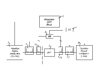
In Fig. 1 a general block diagram is shown of the open loop load pull system.
The
DUT 1 is indicated with two broken lines at each side, which represent the
reference
planes for the DUT 1 at the input and output side. The general blocks
indicated in Fig.
1 will be explained in further detail below.
CA 02722161 2010-10-20
WO 2009/131444 PCT/NL2009/050168
9
Measurement signals are obtained at both sides of the DUT 1 using couplers 4,
5,
with a down-converting linear mixer 55 or IQ demodulator (see Fig. 2a). For
this
frequency down conversion it receives a local oscillator signal from local
oscillator
block 2. The frequency down-converted measurement signals from both the input
side
(source) and output side (load) of the DUT 1 are input to a wideband analog-to-
digital
conversion block 3. As will be described later, this analog-to-digital
conversion block 3
provides eventually the information required to find the necessary signals to
be injected
into the source and load side of the DUT 1. For this injection the waveform
information
is downloaded in arbitrary waveform signal generators, which are part of
injection
signal generators 7, 8 as shown in Fig. 1. Also the intended RF test signal is
downloaded to an arbitrary waveform signal generator, which in the set-up as
shown in
Fig. 1 is considered to be part of injection signal generator 7 (source). The
waveform
generation can be of the IQ type (or a digitally generated IF), the resulting
signals of
these generators are frequency up-converted. The signals needed to control the
reflection coefficients at the different frequency are combined using
frequency
combining networks (e.g. a diplexer of triplexer), which again form part of
the injection
signal generators 7, 8. The resulting signals are presented to the source and
load side of
the DUT 1 using again the coupler blocks 4, 5. Additionally, also a base band
signal
can be generated using base band block 9 and respective couplers 11, 12 for
the source
and load side of the DUT 1. All elements in the present measurement setup use
the
same reference time base, and are fully synchronised.
In Fig. 2a-c, a number of blocks of the block diagram of Fig. 1 are shown in
more
detail. Fig. 2a shows one of the coupler blocks 4, 5, in this case the coupler
block 5 on
the load side of DUT 1. The coupler block 5 comprises a coupler 51, which can
extract
a forward and backward travelling wave from the DUT 1. Each is further split
using
power splitters 52, and input to a mixer 55 (together with suitable local
oscillator
signals from LO block 2). In this manner, signals representing a2,m; a2,2m;
b2,fO; and b2,2f0
are obtained, which are input to the wideband ADC block 3. The frequency
splitting of
the fundamental and higher harmonics in the detection path is done to maintain
the
highest possible dynamic range for the higher harmonics, since filtering out
the
fundamental components reduces the impact of mixer non-linearities when
detecting
the higher harmonics.
CA 02722161 2010-10-20
WO 2009/131444 PCT/NL2009/050168
Fig. 2b shows in more detail the wideband ADC block 3. This block comprises
the actual analog-to-digital converters 31, one for each of the forward and
backward
travelling waves at each of the source and load side of the DUT 1, as well as
one for the
actual source signal (aloop). Furthermore, this block comprises a number of
selectors 33,
5 the function of which will be explained below. The analog-to-digital
converters 31
operate with a first frequency resolution, dependent on the IF down-conversion
and the
sample rate of the analog-to-digital converters 31.
Fig. 2c shows in more detail one of the signal generator blocks 7, 8, more
specifically the signal generator block 8 on the load side of the DUT 1. An
arbitrary
10 waveform generator (AWG) 81 is provided, which uses clock, data and trigger
signals
to generate the I- and Q- parts of the desired waveform. Subsequently, these
are fed to
the frequency up-converting mixers 82. Since the generated signals need to be
frequency converted to the fundamental and harmonic frequencies, the LO signal
to
drive these IQ up-converting mixers must be close to the test frequency for
the
fundamental up conversion and be a multiple for the higher harmonics. To
generate
these signals in a phase coherent fashion multipliers 83, 84 are used to up-
convert the
LO signal. If necessary, possible leakage of local oscillator signal in the
mixer 82 may
be suppressed using DC-offsets. In a specific embodiment, which is useable for
single
tone testing of a DUT 1, the combination of AWG 81 and IQ mixer 82 is arranged
as a
single side band up-converting mixer.
Switchable attenuators 85 are provided to be able to make optimum use of the
dynamic range of the digital-to-analog conversion in the AWG's 81. Via buffers
/ RF
amplifiers 86, the generated signals are combined in a frequency (de-
)multiplexing
filter 87 for signal injection into the source and load side of the DUT 1. The
frequency
de-multiplexing filters 87 are used to bring the injection signals for
controlling the
reflection coefficients for the fundamental and harmonic frequencies together.
For each
frequency (fundamental and harmonics), a separate AWG 81 is used, allowing to
create
the amplitude controlled synchronized coherent injection signals for realizing
the
fundamental and higher harmonic reflection coefficients. A similar hardware
implementation may be used for the generation of the base band signal in base
band
block 9 of Fig. 1, but now directly using an arbitrary waveform generator, a
low pass
filter, a switchable attenuator and an amplifying buffer. The base band
signals are then
directly input to the bias T circuitry of couplers 11, 12. The AWG's 81
operate with a
CA 02722161 2010-10-20
WO 2009/131444 PCT/NL2009/050168
11
second frequency resolution, which is an integer multiple worse than the first
frequency
resolution associated with the analog-to-digital converters 31.
The connection scheme of the units needed to create the synchronized and
coherent injection signals at the desired frequencies at the source and load
side of the
DUT 1 is given in the block diagram Fig. 3. Here it is indicated that it is
possible to
generate not only baseband and fundamental frequencies, but also second, third
and
even higher harmonics (up to an Nth harmonic). A combination of one AWG 81,
mixer
82, switchable attenuator 85 and buffer 86 is shown in this block diagram as
an
amplitude controlled synchronized and coherent source (ACSCS) 15, which
receives
the clock, trigger and data signal, and an attenuator control signal, and
outputs an
amplitude controlled, synchronized and band modulated signal. Likewise, a
combination of an AWG 81, low-pass filter, switchable attenuator 85 and buffer
86
forms a baseband signal injection circuit (BIC) 16. The BIC receives as input
the clock,
trigger and data signals, and an attenuator control signal, and outputs an
amplitude
controlled synchronized baseband modulated signal.
As indicated in the block diagram of Fig. 3, a single ACSCS 15 is used to
provide
the source signal for DUT 1, and a number of ACSCS blocks 15 is used to
provide the
signals for the source side of the DUT 1. These blocks may be considered as
comprised
in the injection signal generator 7 on the source side of the DUT 1 as
depicted in Fig. 1.
Furthermore, the BIC 16 is comprised in baseband block 9, and fed to the DUT 1
using
coupler 11 (e.g. using a bias T circuitry). Likewise, also a number of ACSCS
blocks 15
are used to provide the test signal at the load side of DUT 1, and are
considered as
comprised in the injections signal generator 8 on the load side of the DUT 1
in Fig. 1.
Again, the single BIC 16 is comprised in baseband block 9 of Fig. 1, and fed
to the
DUT 1 using coupler 12 (e.g. again using a bias T circuitry).
The circuitry hardware described above offers load pull device
characterization
with absolute control of the reflection coefficients versus frequency in
baseband, and
the frequency bands centered at the fundamental and harmonic frequencies at
the input
and output of the device under test 1. The proposed measurement concept can
compensate for losses and phase delays present in the couplers, connecting
cables and
other components of the measurement setup, as well as it can easily correct
for non-
linearity imperfections of the amplifiers. Due to its architecture it can also
facilitate
CA 02722161 2010-10-20
WO 2009/131444 PCT/NL2009/050168
12
pulsed device characterization. However, to be operated correctly in a useful
way, the
signal content of the injection signals need to be determined
Ideally the following conditions which are desired to be established for a
given
device under test 1 are formulated through:
ax n (.fx,n) = bx n (.fx,n) F n (.fx n )
in which:
x = index source (s) or load (1)
n = frequency index: baseband (0), fundamental (1), harmonic (2 and up)
I'x,n (f,'.) = an arbitrary user defined function for reflection coefficient
of the
source (aa,n) or load (bx,n) versus frequency at the baseband or fundamental
or
harmonic frequency.
The exact waveforms to be loaded in the Arbitrary Waveform Generators 81 for
creating the injection signals are found by enforcing a user defined
reflection
coefficient versus frequency function (spanning at least a control bandwidth
around
each of the fundamental and harmonic frequencies). The frequency domain
observed is
divided in frequency bins. This may be illustrated by an exemplary test set-up
for a
DUT 1 operating in a W-CDMA environment, which in this case has a fundamental
frequency f0=2.14GHz. A total control bandwidth of 20.4 MHz was used in this
experiment. For the AWG's 81, a sampling frequency of 144MHz was used with a
record length of 24000 samples. For the AWG 81 this results in a frequency
resolution
of 6 kHz (i.e. the bin spacing for generation of signals). For the A/D
converters in the
wideband ADC block 3, a sampling frequency of 100MHz was applied, and a record
length of 2 * 106 samples. This results for the measurement part in a
frequency
resolution of 50 Hz, i.e. the total number of controlled frequency bins in
this
experiment was 3401 (3401 * 6 kHz providing the 20.4 MHz total control
bandwidth).
By monitoring the deviation of the desired reflection coefficient with the
actual
measured reflection coefficient for each frequency bin, the spectrum of the
injected
wave (source and load) is optimized and found by subsequent iterations. The
spectral
power densities of the incident and emanating waves from the active device
(DUT 1)
needed in this calculation are captured through using down-conversion to a low
IF
CA 02722161 2010-10-20
WO 2009/131444 PCT/NL2009/050168
13
frequency using a highly linear mixer 55 and are subsequently digitized using
wide-
band analog-to-digital converters 31. Alternatively, it is also possible to
capture the
waves through direct down conversion to baseband by using highly linear IQ
mixers 55
and wide-band analog-to-digital converters 31 to sample the down-converted I
and Q
waveforms. The use of wideband analog-to-digital converters 31 allows
capturing at
once of all the frequency bins for the bandwidth of interest, which should
provide
sufficient frequency resolution in the optimization / iteration of the
spectral content of
the injection signals. By changing the LO frequency for the down conversion
(in LO
block 2, see Fig. 1) the subsequent reflection coefficients for the frequency
bands
around the fundamental and higher harmonics can be determined (using the
selectors
33, see Fig. 2b). The base band information can be directly digitized (see
also Fig. 2b).
The iterative process as mentioned above will now be discussed in more detail
with reference to the flow diagram as shown schematically in Fig. 4. As
mentioned the
exact waveforms to be injected are determined based on satisfying the
reflection
coefficients at the reference planes of the device under test 1 (step 41). The
starting
point in this process can be an initial reflection coefficient measurement,
when no
injection signal is applied. As an alternative, a first guess is made of the I
and Q
waveforms for the injection signals a and b in the frequency domain (step 42).
An
inverse FFT of the I and Q waveforms is executed (e.g. in a processing system
which
may be part of the wideband ADC block 3 in Fig. 1), and the time domain I and
Q
coefficients are input to the AWG's 81 (step 43). Subsequently, the
measurement is
executed, and measurement data of the waveforms is obtained from the A/D
converters
31 in step 44. Again, the measured waveforms are submitted to an FFT operation
(e.g.
again using the processing system in wideband ADC block 3 in Fig. 1), and the
actual
reflection coefficient (F) as a function of frequency is determined in step 45
(i.e. using
the frequency bins as discussed above). The actual measured F function is
compared to
the desired F versus frequency function, and an error function is calculated
(step 46). If
the error function exceeds a threshold level (indicated by `desired error' in
decision
block 47) a new smart guess is made for the I and Q versus frequency (block
48) and a
new measurement cycle is started in block 43. If the determined error function
is below
the threshold level, the iteration algorithm is ended in block 49. Note that
the proposed
method can accurately control the reflection coefficients / gammas in phase
and
CA 02722161 2010-10-20
WO 2009/131444 PCT/NL2009/050168
14
magnitude over a large frequency band, without being hampered by the
electrical delay.
In fact the reflection coefficients can be chosen arbitrary as function of
frequency.
Consequently the desired waveforms are found through optimization or iteration
techniques for each injection signal (baseband, fundamental, harmonics, source
side
and load side of DUT 1). In an advanced implementation this iteration can be
based on
circuit simulator principles, which aim to satisfy the boundary conditions of
the device
under test 1 simultaneously for all harmonics and/or an envelope of the
modulated
signal. This later technique will most likely reduce the number of required
iterations
and consequently will improve measurement speed.
It is important to stress that the proposed invention embodiments are not a
time
continuous system and do not make use of (real time) feedback loops. For this
reason
the system does not require any synchronization between the analog-to-digital
converters 31 used for the reflection coefficients measurements and the
Arbitrary
Waveform Generators 81 used for creating the injection signals. In the
embodiments
described above, synchronization is implemented, and this is beneficial if pre-
distortion
of the input signal is desired (e.g. to compensate for the non-linear
behaviour of the
input drive amplifier or the non-linearities of the DUT 1 itself). Also, as
opposed to
closed loop load pull configurations, due to the fact that the desired
reflection
coefficients are found by subsequent iterations, the loop/buffer amplifiers 86
used for
injecting the fundamental and harmonic signals are no longer required to be
linear,
since the influence of their non-linearities will vanish in subsequent
optimization of the
reflection coefficients. Consequently, the present embodiments are not bounded
by the
restrictions related to causal systems which apply to closed loop systems. In
the present
embodiments, waveforms are used, which are composed out of a repeated data
record,
which is in general different for all digital-to-analog created injection
signals a, b.
However, as discussed earlier, all signals created for injection to the device
under test 1
need to share the same time base and must be fully synchronized.
Since in the proposed version of a load pull open loop system it is possible
to
make use of the full waveform record of the source signal and its related
reflection
coefficients over time, advanced knowledge on the signal events in time is
available
when iterating for the new injection signals to be fed to the device under
test 1. As a
result, it is possible to compensate for phase and amplitude errors as well as
for phase
delay caused by linear and non-linear distortion phenomena. This is a unique
feature of
CA 02722161 2010-10-20
WO 2009/131444 PCT/NL2009/050168
the proposed open loop system. Note that these principles will fail in a
feedback
approach to compensate for the electrical delay, simply because in a time
continuous
feedback system this is impossible.
Consequently, in contrast to other prior art proposed solutions, the present
5 solution facilitates the use of arbitrary reflection coefficients within a
given signal
bandwidth, independently for the fundamental and harmonics and even baseband
conditions of the device under test 1. This is only possible due to the open
loop
architecture which relieves the basic limits of implementing a causal
function. The use
of independent AWG's 81 for the generation of the injection signals is a
necessary
10 condition to test the large-signal operation of practical devices, without
making pre-
assumptions on their electrical behaviour. The proposed approach also
automatically
overcomes the non-linearity limitations that are normally related to the
amplifiers used
in an active harmonic load pull system, since these non-linearities will be
automatically
compensated for in the optimization / iteration of the waveforms of the
injection signals
15 in the aim to simply satisfy the predefined user settable relations of
reflection
coefficients over frequency for the baseband, fundamental and higher
harmonics.
In a further embodiment, the same frequency binned optimization approach can
be also applied to pre-distort the test signal for the device under test 1 to
compensate
for the non-linearities of the power amplifiers used in the input path of the
system, by
smart injection of a signal comprising frequency components that cancel the
distortion
products. In this case the exact waveforms to be loaded in the Arbitrary
Waveform
Generators 81 for creating the input signal to the device under test 1 are
found by
enforcing a user defined amplitude and phase of the test signal versus
frequency. By
monitoring the deviation of the desired amplitude and phase of the input
signal for each
frequency bin with the actual measured amplitude and phase, the spectrum of
the
injected wave is optimized and found by subsequent iterations. Note that this
approach
requires the synchronization of the Arbitrary Waveform Generators 81 with the
analog-
to-digital converters 31 in order to be able to measure also the phase of the
injected
wave.
The frequency resolution for the D/A generated signals (using AWG's 81; second
frequency resolution) is, in further embodiments, effectively the same to that
of the
digitized waveforms by the A/D converters 31 (first frequency resolution), as
is
expressed by the equation below.
CA 02722161 2010-10-20
WO 2009/131444 PCT/NL2009/050168
16
fSA_D - A.fAWC - 1 /sAWC = 1
NA D k k NAWC k - TMOD
where:
AfA/D = frequency resolution of the A/D converters (first frequency
resolution)
Af AWG = frequency resolution of the D/A converters (second frequency
resolution)
k = integer
TMOD = time period of the input signal that allows to meet the requirements of
the modulation standard according a given test model
fsAJD = sampling frequency of the A/D converters 31
NAID = number of samples used by the A/D converters 31
fsAwG = sampling frequency of the Arbitrary Waveform Generators 81
NAWG = number of samples used by the Arbitrary Waveform Generators 81
This frequency resolution depends on the sampling frequencies and the number
of samples for both the synchronized D/A converters in AWG's 81 as well as the
A/D
converters 31. In principle the frequency resolution of the A/D converters 31
can be an
equal to or better than the D/A converters in AWG's 81. This is expressed by
the
factor k, which in this embodiment is an integer number. In an alternative
embodiment,
the factor k can also be a real number larger or equal to 1. If k >1, signal
processing
techniques have to be used to make the effective frequency resolution of the
acquired
signals match that of the D/A converters in the AWG's 81.
The spectral information in the frequency bins for the acquired waveforms
provide information of the reflection coefficients versus bandwidth. It is
this
information that is used in the iterations / optimization of the injection
signals. For this
purpose frequency mapping is applied to overcome the frequency offsets
introduced by
the mixed IQ / low-IF approach. It must be mentioned that for the acquisition
path no
phase coherence is required with the signal generation. In fact, if it is
desired to capture
a frequency band, around the fundamental or harmonics of interest, larger than
the
bandwidth of the acquisition A/D converters 31 would allow for, the LO
frequency
(from LO block 2, see Fig. 1) used for down conversion can be shifted,
bringing
another part of the frequency spectrum in reach of the A/D converters 31.
Stepping of
CA 02722161 2010-10-20
WO 2009/131444 PCT/NL2009/050168
17
the LO frequency for the down conversion of the signals to be acquired is also
done for
measuring the reflection coefficients at the harmonic frequencies.
With the techniques of the embodiments as described above all relevant
information of the reflection coefficients offered to the DUT 1 can be
collected and
used as input in the iteration / optimization process in achieving the optimum
injection
signals, facilitating the user with free to specify matching conditions within
the
frequency bands of interest.
In the particular case of iterating / optimizing the input signal to
compensate for
the input path amplifier distortion products, additional information of the
phase of the
input signal is needed. For this, in a further embodiment, the Arbitrary
Waveform
Generators 81 need to be synchronized with the Analogue-to-digital converters
31
through the use of a marker / trigger (trigger signal as depicted in Fig. 1-3)
to allow
extraction of the wave phase information. Furthermore, when the bandwidth of
the
input signal to pre-distort is larger than the bandwidth of the acquisition
A/D converters
31 would allow for, the LO frequency used for down conversion can be shifted,
bringing another part of the frequency spectrum in reach of the A/D converters
31. In
this case, though, also the phase change in the LO frequency stepping must be
tracked,
through the extra measurement of a reference IF sine wave that can be obtained
by
direct down-conversion of an RF reference signal (phase coherent with the
input and
the injection) with the LO frequency.
Note that the controllable signal bandwidth of the digital-to-analog
converters in
the AWG's 81 (usually implemented using commercially available D/A cards)
should
exceed the requirements of the modulation standard to be tested for. This can
be
understood as follows. The original modulated signal provided by the source
will (in
the case of a transistor as DUT 1) not only be amplified by the DUT 1 but also
distorted, causing IM3 and IM5 related frequency products as well as higher
harmonics. These frequency mixing products expand the bandwidth of the
original
signal. Consequently, in order to be able to offer the proper / realistic
reflection signals
also for these frequency mixing products, the bandwidth that can be controlled
by the
injection signals should be significantly larger than the bandwidth of the
modulated
source signal itself This is illustrated in the power spectrum graphs as
plotted in Fig. 7,
which show frequency considerations related to the source signal generation,
and the
injection signals at the fundamental and 2nd harmonic assuming low IF
frequency
CA 02722161 2010-10-20
WO 2009/131444 PCT/NL2009/050168
18
down-conversion of the frequency bands of interest around the fundamental and
harmonics.
As shown in the block diagram of Fig. 1, 2b and 2c, data is transmitted from
wideband A/D converters 31 to the AWG's 81. As the measurement system is
usable
for high frequencies and complex modulation schemes, such as W-CDMA signal
testing, the data amount transmitted can be very large. In a practical
implementation
this can be met using fast datalinks between the various hardware cards, e.g.
using PXI
or PXI express interfaces.
Although the above embodiments of the present invention have been described
for a DUT 1 having a source side and a load side requiring single ports each,
the
invention may also be applied in measurement system implementations for
testing
multi-port devices, such as three port or four port devices.
In a further embodiment, the reflection coefficients can be defined not only
versus frequency for the frequency bands around the fundamental and harmonic
frequencies at input and output (static condition) but can be also defined to
follow a
pre-described trajectory versus time (dynamic condition). Note that such a
feature
would allow the operator of the load-pull system to mimic realistic circuit
conditions
that occur in high efficiency amplifiers that use load modulation. Examples of
these
amplifiers are: Doherty, LINC or dynamic loadline amplifiers. In these
amplifiers the
effective load (reflection coefficient changes with the envelope of the
modulated input
signal, in order to optimize the voltage swing over the output stage yielding
an increase
in amplifier efficiency. Note that the proposed hardware setup allows such a
feature,
only the optimization algorithm for the reflection coefficients need to be
modified in
order to handle the time varying reflection coefficients.
Examples
The functionality of such a load-pull characterization system is demonstrated
in
Fig. 5a and 5b which show the uncorrected (a) and corrected (b) reflection
coefficient
offered to the device under test 1 output for a 14 tone input signal with 15
MHz
bandwidth in the form of Smith-charts. Both the input signal, as well the
injection
signals are generated using the synchronized AWG's 81, which use the same
clock and
data record length to store the waveforms. All signals are coherently up-
converted as
CA 02722161 2010-10-20
WO 2009/131444 PCT/NL2009/050168
19
described with respect to Fig. 2c. In Fig. 8 a spectral diagram is shown of
this 14 tone
input signal, centered at 2.14 GHz. Fig. 5a shows measured reflection
coefficient of 14
frequency tones in the proposed active load pull system over a frequency
bandwidth of
15 MHz, when no compensation is present for the electrical delay and gain
variation in
the load pull system over this frequency range. So in this case the injection
signals are
not found by optimization for each tone, but set similar to the conditions
needed for
achieving FL=1 for the central frequency. Consequently, note that only at the
central
frequency of 2.14GHz the intended reflection condition (TL=1) is achieved. In
Fig. 5b
the results are shown when the electrical delay and gain variations are
compensated in
the digital domain by using iteration / optimization techniques as described
above for
the 14 frequency tones to achieve the desired reflection condition (FL=1) for
all
frequencies. Note that now for all frequencies the intended reflection
condition (TL=1)
is achieved.
The use of complex modulated signals is also feasible. In this case the
waveform
used as an input signal preferably meets all the requirements of the
modulation standard
as defined by the test models for the various communication standards. This
requires
that the record length used to store all the modulated waveforms (both for
driving input
source signal as well as all the injection signals), should be equal and long
enough in
order to contain a full period of the test model for the complex modulated
signal of
interest. An example of a W-CDMA test signal is shown in the bottom graph of
Fig. 6,
which has a fundamental frequency f0=2.14GHz. A total control bandwidth of
20.4
MHz was used. For the A/D converters in the wideband ADC block 3, a sampling
frequency of 100 MHz was applied, and a record length of 2 * 106 samples. This
results for the measurement part in a frequency resolution of 50 Hz, i.e. the
total
number of frequency bins in this experiment was 3401 (3401 * 6 kHz providing
the
20.4 MHz total control bandwidth. For all these frequency bins the magnitude
and
phase of the (in this case) output reflection coefficient is plotted as well
in the top two
graphs of Fig. 6. Note that the proposed method can accurately control the
reflection
coefficients / gammas in phase and magnitude over a large frequency band,
without
being hampered by the electrical delay. In fact the reflection coefficients
can be chosen
arbitrary as function of frequency. In the bottom graph of Fig. 6 the "control
noise
floor" is indicated as well. Above this level the signal levels are high
enough to
accurately control the gamma as function of frequency both in phase and
magnitude,
CA 02722161 2010-10-20
WO 2009/131444 PCT/NL2009/050168
below this level, the received signals are considered to be too noisy and no
power is
injected to control the reflection coefficients. This yields high fluctuations
of the
reflection coefficients, however due to the very low "noise like" signal
levels these
fluctuations are not important and do not influence the measurement. When
increasing
5 the power levels and further reducing the noise floor the reflection
coefficients can be
controlled over a even larger range since the signals are now higher than the
control
noise floor. Note the very high dynamic range achieved which underlines the
benefits
from the proposed setup.
10 Fig. 9 shows an exemplary set-up of the open loop load pull arrangement as
used
in a further exemplary embodiment. In this embodiment, only the fundamental
frequency and a second harmonic thereof is used for generating the source,
load and
input injections signals to the device under test 1. Similar as in the
schematic diagram
of Fig. 1, reflection coefficients are determined at calibration reference
planes at the
15 input and output side of the device under test 1, indicated by dashed
lines. The
generated signals are injected at the device under test 1 using probes 1 a (as
known to
the skilled person).
The generated signals arrive at the probes 1 a from an input section 4a and
output
section 5. Source signals are generated using a source injection signal
generator 7a, and
20 input to the input section 4a. An input signal for the device under test 1
is generated by
an input injection signal generator 7b, and coupled to the source injection
signal using a
signal input section 4b and the input section 4a. The signal input section 4b
is also
arranged to provide measurement data related to the input signal (indicated by
aYef and
obtained from the input signal using the synchronized local oscillator signal
LO). The
load injections signal is generated using load injection signal generator 8
coupled to the
output section 5. The signal generators 7a, 7b, 8 operate in a similar manner
to the
corresponding blocks 7 and 8 in Fig. 1 using AWG's as discussed in the
corresponding
embodiments above.
Furthermore, a wideband ADC block 3 is provided as in the embodiments
described above. As indicated in Fig. 9, now only the coefficients a1, b1, and
a2, b2 are
derived from the injections signals and fed to the wideband A/D converters 31.
In this embodiment, a new simple but very effective mixed-signal approach is
provided that enables fully-controlled, multi-dimensional parameter sweeps,
while
CA 02722161 2010-10-20
WO 2009/131444 PCT/NL2009/050168
21
being able to control all other non-swept parameters to their user predefined
values.
Using this embodiment it is possible to perform high speed device
characterization over
an arbitrary multi-dimensional parameter sweep using well defined discreet
measurement points. For example, device characterization with swept discreet
input
power points and arbitrarily swept discreet fundamental loading points is
possible,
while simultaneously controlling all other (harmonic) source and loading
conditions to
their user pre-defined values. The proposed functionality results in extremely
fast as
well as very accurate and well defined large-signal device characterization,
features
that are highly beneficial in the power amplification (PA) design process.
Traditional load-pull measurement techniques are recognized to be of
fundamental importance for the large-signal characterization of high-frequency
devices,
allowing to determine the optimal power amplifier (PA) loading conditions, for
any
given large-signal quantity (e.g. Gain, Output Power, PAE, intermodulation
distortion
etc.). Nevertheless, both passive and active techniques are highly demanding
in terms
of measurement time, especially when it is desired to monitor and control
multiple
parameters simultaneously, such as fundamental and harmonic terminations, at
multiple
input power levels. This is usually reflected in extremely long measurement
times and
slows down the PA design/optimization process.
It is noted that recently several works have been reported in literature,
which
propose "real-time" load-pull solutions by synthesizing load reflection
conditions
through analogue modulation techniques (see e.g. the already mentioned US
patent
application US2007/0194776). All these techniques provide "real-time" a set of
load
reflection coefficients to the device-under-test (DUT) by injecting into the
device a
signal composed of one or more frequency components which are offset with
respect to
the fundamental frequency of the DUT. Although very good results have been
achieved
with these techniques, their analogue nature still imposes limitations on how
many
parameters, and how well these parameters (including the non swept ones) can
be
controlled for their value and/or sweeping range.
The arrangement as provided in this embodiment of the present invention is
originally developed to handle wideband complex-modulated signals, makes use
of
wideband analogue-to-digital converters to capture in one single acquisition
the
incident and reflected waves at the DUT reference planes I a. Furthermore, the
fundamental and harmonics source and loading conditions offered to the DUT 1
are
CA 02722161 2010-10-20
WO 2009/131444 PCT/NL2009/050168
22
synthesized by injecting signals that are generated by base-band arbitrary-
waveform-
generators and up-converted using in-phase/quadrature (IQ) modulators.
In this embodiment the capability to coherently synthesize any arbitrary
signal at
the fundamentals as well as at the harmonics is used to generate an
(arbitrary)
sequenced range of input power levels and load conditions in one single-shot
measurement, as explained in detail in the following.
In an open-loop active load-pull measurement arrangement (e.g. the one shown
in
Fig. 9), a signal with controlled phase and amplitude is injected to present
to the
device-under-test 1 a synthetic user specified reflection coefficient. Since
in this fully
coherent system (as indicated by the use of fo, 2f0 and LO throughout the
arrangement)
it is possible to generate any combination of arbitrary injection signals. The
waveforms
to be injected into the DUT 1 can be defined at the fundamental and harmonics
frequencies, such that they contain multiple sinusoidal time-segments with
different
amplitude and phase information. This approach facilitates the generation of
any
arbitrary chosen succession of synthesized load and source terminations, both
at the
fundamental and harmonic frequencies. Also the test signal driving the DUT 1
is
generated in the same way with multiple wave segments that can represent
different
power levels. The measurement is taken by acquiring all the sequenced
waveforms in a
single shot with wideband analogue-to-digital converters (in block 31), and by
processing every time-segment independently.
It is important to stress that, in contrast to the disclosure of US patent
application
US2007/0194776, all the waveforms used in the time-segments to be injected at
the
input, source and load for the fundamental are pure sinusoidal signals with a
stele
constant frequency that is equal to the fundamental operating frequency f0 of
the device
under test 1. While the frequency of the signals to be injected for the
harmonics are
exactly equal to these harmonics (i.e. 2f0) of the device under test 1. The
actual
parameter sweep is performed by setting the discreet power and loading
conditions
through the phase and amplitude conditions of the various time segments.
In order to track accurately the sequenced time segments the data-acquisition
part
of the measurement arrangement must be fully synchronized with the data-
generation
part of the measurement arrangement (e.g. through a 10 MHz reference,
indicated as
LO). Furthermore, the measurement arrangement uses a trigger that indicates
the
beginning of the sequence time segments with the stepped power and load
states.
CA 02722161 2010-10-20
WO 2009/131444 PCT/NL2009/050168
23
Fig. 2 shows an example of a time-segmented modulated RF wave, where four
different loads are presented to the DUT 1 at two different power levels. The
big
advantage of this time-segmented method is that multi-dimensional parameter
sweeps
can be executed in a single shot of the signal generation and data acquisition
hardware,
while the coherency of the measurement arrangement and some book keeping
tracks
the information embedded in the individual wave segments. This approach
completely
eliminates settling times that dominate the overall time in conventional load-
pull
measurements, while providing a more sophisticated control than what is
possible with
analogue load modulation methods.
Although a single measurement execution of such a parameter sweep takes only a
fraction of a second, something that would already result in an effective load
and power
sweep, practical situations quite often require accurately controlled power
and load
conditions. In an open loop system this can only be achieved through
successive
iterations. In view of this, the coherent mixed-signal IQ generation in the
present
measurement arrangement embodiment allows to optimize the individual time-
segments of the IQ waveforms independently. This is done in a similar way as
discussed with reference to Fig. 4 above. In this embodiment, an entire IF
waveform is
acquired, but every time segment is processed separately to calculate the
gamma for
every segment (cf. block 44 and 45 in Fig. 4). Subsequently, the measured
gamma is
compared to a desired gamma for every segment, resulting in a gamma error for
every
segment (cf. block 46 in Fig. 4. In an iterative loop, the I and Q time
segments are
recalculated based on the gamma error to compose a new injected waveform (cf.
block
49 in Fig. 4).
This offers full control of the applied loading and power conditions to which
the
DUT 1 is subjected. Note that, for example, this feature can be used to target
any given
area on the Smith plane, while at the same time sweeping the input power.
These multi-
dimensional parameter sweeps, embedded in the recorded waves of the arbitrary
waveform generators that drive the IQ modulators, are at least two orders of
magnitude
faster than a conventional approach using only one signal condition at the
time to
construct a parameter sweep.
To demonstrate the functionality of the realized setup, an LDMOS device was
measured at 2.14 GHz with a gate width of 1.8 mm. A drain current and voltage
of 13
mA and 28 V respectively were used.
CA 02722161 2010-10-20
WO 2009/131444 PCT/NL2009/050168
24
It has been found that this measurement arrangement has the capability to
obtain
with excellent precision (this in contrast to previous solutions) any
arbitrary controlled
source and load impedance state at the fundamental and harmonic frequencies.
In this
example the fundamental-load termination provided to the DUT is swept, the
source
fundamental is kept constant at the value FS = 0.5Z900, while the 2nd harmonic
load
and 2nd harmonic source terminations are kept constant to an open circuit
condition.
Note that this control of the non-swept parameters is desired when evaluating
active
device performance for different types of amplifier classes (in this case
inverse class-
AB).
The ability to select any arbitrary range of reflection coefficients is
particularly
useful when one wants to only characterize selected areas of the device 1
source or load
terminations in the Smith chart, e.g. when avoiding regions where the device
behaves
potentially instable, or when one wants to avoid loading conditions that can
yield
failure of the DUT 1 (voltage or thermal breakdown). This is far from trivial
when
using analogue load modulation methods as used in prior art set-ups.
An example of such a complex measurement is shown in Fig. 1 la and b. Here
first the output stability circle was obtained from the small signal S-
parameters, after
which only the region outside the instable region was addressed in the actual
measurement by a fundamental load sweep at various (much higher) power levels.
The
resulting measured output power contours of the LDMOS device for 13 dBm source
available power have been plotted in Fig. I la. The measured gain as function
of input
power for the different loading conditions is plotted in Fig. 1lb (source and
harmonic
loading conditions were kept identical to those described before). In this
measurement
the output power of the device 1 has been obtained for 50 load states at 21
levels of
input power. Although a single measurement of the wave segments of these 1050
points only takes a fraction of a second (in this example wave segments were
used with
a length of 1.6 s, resulting in 1.68 ms for the total record length), here
the total
measurement time (including iterations) needed from scratch to reach the
final, user
pre-defined, controlled input power, fundamental and harmonic source and load
reflection coefficients conditions for all 1050 points takes less than 2
minutes. This
time span can be reduced even further by optimizing the software for speed.
In the approach as described, very fast stepping from one signal condition to
the
next one occurs. However at each moment in time the injection frequency is
equal to
CA 02722161 2010-10-20
WO 2009/131444 PCT/NL2009/050168
that of the source signal f0 or one of its harmonics. All these segments are
placed in
sequence and in one shot all the signal conditions are measured with a wide
band
receiver. Note that this would not be possible with a classical narrowband
network
analyzer, which would suffer from the sharp transitions from one time segment
to the
5 next one. This approach requires a very good synchronization of all
injection signals,
but also the signal acquisition needs to be fully synchronized with the
injection signals
and lined up such that within the acquired data segments no transitions in
phase or
amplitude of the purely sinusoidal signal are present .
In practice when monitoring the spectrum of the injection signals on a
spectrum
10 analyzer, the phase and amplitude changes from one segment to the next time
segment
will cause various frequency components on the spectrum analyser screen, but
these
components would have an almost random character and will play no role at all
in the
functioning of the present embodiments.
Note that within one time segment there is only the fundamental and (when
using
15 a harmonic system) harmonic frequencies present and no offset frequencies.
This situation is somewhat equivalent with the classical open loop situation.
However, in a classical open loop load pull setup, the change in amplitude and
phase
relations are mostly done by phase shifters and attenuators, which are much
slower. If a
"conventional setup" makes use of an IQ approach (or vector source) than the
data
20 acquisition was never fully synchronized or sufficiently wide band in prior
art
arrangements, which makes it impossible to implement the proposed approach
with
such a short sequenced time segments.