Note: Descriptions are shown in the official language in which they were submitted.
CA 02723742 2010-11-05
WO 2009/135298 PCT/CA2009/000610
Optical Image Reader
FIELD OF INVENTION
[0001 ] The present invention relates to optical devices, and more
specifically to a system for
image-reading an indicia on the object.
BACKGROUND OF THE INVENTION
[0002] Handheld imagers are well known in the art. The imagers typically
include a targeting
system having a light source for illuminating a target object, an image sensor
for sensing
reflection from the object, and a signal processor for processing the output
from the image
sensor.
[0003] Considerable effort has been made into the handheld imagers. However,
many issues
still remain with regard to, for example, response time, power consumption,
quality of
imagers.
SUMMARY OF THE INVENTION
[0004] It is an object of the invention to provide a method and system that
obviates or
mitigates at least one of the disadvantages of existing systems.
[0005] According to an aspect of the present invention there is provided a
targeting system for
an imager. The targeting system includes a light device having a plurality of
light emitting
diodes (LEDs), each for emitting light. The targeting system includes a device
for shaping a
single targeting light based on the outputs of the plurality of LEDs.
[0006] According to another aspect of the present invention there is provided
an image system
for capturing image of an indicia on an object. The image system includes a
targeting light
source for providing a targeting light to the indicia on the object, and an
optical system for
focusing reflection from the object. The optical system includes a liquid
focus lens element
having a variable focus, and a controller for controlling the focus of the
focus lens.
[0007] According to a further aspect of the present invention there is
provided a system for
capturing an image of a barcode on an object. The system includes an image
sensor for
CA 02723742 2010-11-05
WO 2009/135298 PCT/CA2009/000610
sensing reflection from the object, and an ambient light sensor for sensing
the reflection from
the object prior to the sensing by the image sensor to calculate a first
estimate for exposure of
the image sensor.
[0008] According to a further aspect of the present invention there is
provided a barcode
reader, which includes a light source for providing a light to an object
having a barcode, an
objective lens for receiving reflection from the object, and a holographic
diffuser for changing
the angle of the light source.
BRIEF DESCRIPTION OF THE DRAWINGS
[0009] These and other features of the invention will become more apparent
from the
following description in which reference is made to the appended drawings
wherein:
Fig. 1 is an exploded view of an example of an imager in accordance with an
embodiment of the present invention;
Fig. 2 is a perspective front view of a housing for the imager of Fig. 1;
Fig. 3 is a perspective rear view of the housing for the imager of Fig. 1;
Fig. 4 is a perspective rear view of the housing with a laser for the imager
of Fig. 1;
Fig. 5 is a perspective front view of the housing with the laser for the
imager of Fig. 1;
Fig. 6 is a perspective rear view of the housing with a LED aperture for the
imager of
Fig. 1;
Fig. 7 is a perspective view of a PCB assembly for the imager of Fig. 1;
Fig. 8 is a perspective view of a variable focus lens element system for the
imager of
Fig. 1;
Fig. 9 is a perspective view showing a flex cable and temperature sensor for
the imager
of Fig. 1;
-2-
CA 02723742 2010-11-05
WO 2009/135298 PCT/CA2009/000610
Fig. 10 is a perspective view of an illumination diffuser board for the imager
of Fig. 1;
Fig. 11 is a perspective front view of a front panel for the imager of Fig. 1;
Fig. 12 is a perspective front view of the imager of Fig. 1;
Fig. 13 is a perspective rear view of the imager of Fig. 1;
Fig. 14 is a flow chart showing a method of assembling the elements of the
imager of
Fig. 1;
Fig. 15 is a block diagram illustrating the imager of Fig. 1 and a signal
processor;
Fig. 16 is a block diagram illustrating an example of a PCB design applicable
to the
imager of Fig. 1.
DETAILED DESCRIPTION
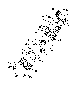
[0010] An example of an imager 2 in accordance with an embodiment of the
present
invention is shown in Figs. 1-15. Referring to Figs. 1-15, the imager 2 has a
plurality of
components for capturing and reading optical indicia (e.g, bar code, other
symbology) on an
object. The imager 2 may be a barcode scanner/reader.
[0011 ] The imager's components include a printed circuit board (PCB) assembly
30 having an
illumination device for illuminating an object and an image sensor 34 for
sensing reflection
from the object, a targeting/aiming light device 50, 80 for providing a
targeting light to an
indicia on the object, a sensor focus lens system 60, 70 for focusing the
reflection from the
object, an illumination diffuser board 90 for diffusing the illumination, a
cylindrical lens 130
for shaping the targeting light, and an ambient light sensor 110 for
calculating the first (initial)
estimate of exposure for the image sensor 34.
[0012] The imager's components further include a housing 10, a front (top)
cover panel 120
and a binding system 140 for assembling. The front side of the housing 10 is
formed to
assemble the focus lens system 70, the illumination diffuser board 90, the
cylindrical lens 130,
-3-
CA 02723742 2010-11-05
WO 2009/135298 PCT/CA2009/000610
and the front panel 120. The rear side of the housing 10 is formed to assemble
the focus lens
system 60 and the PCB assembly 30.
[0013] The imager 2 can alternatively accommodate either a LED array 50 or a
laser assembly
80 as the targeting/aiming light device, in order to improve targeting/aiming.
The LED array
50 includes a plurality of LEDs 52 that are mounted on the PCB 32 of the PCB
assembly 30
and form a linear LED array. In this example, three LEDs 52 form the LED array
50,
however, the number of LEDs and its shape may vary. The laser assembly 80
includes, for
example, a laser diode, collimating lens and driver.
[0014] The targeting/aiming system of the imager 2 includes one or more post
lens apertures
(e.g., 222 of Fig. 6, 122 of Fig. 11) to sharpen ends (define edge) and
prevent fade-off
phenomenon. The post lens aperture is formed so that a desired
targeting/aiming pattern
(light) is projected onto a target. In this example, the post lens aperture is
a single shaping slot
or has a rectangular shape to project a horizontal line onto the target. In
this example, a
horizontal line (e.g., red line) light is provided by either the LED array 50
or the laser
assembly 80.
[0015] The imager 2 can also alternatively accommodate either a focus lens
element system
60 or a focus lens element system 70, as the sensor focus lens system. In this
example, the
focus lens system 60 includes a multi-element achromatic lens element (62)
with a certain
fixed lens focus. In this example, the focus lens system 70 includes a fluid
(liquid) lens
element (74) with a variable lens focus. The imager 2 can use two different
image optics (62,
74) for best-focusing target indicia onto the image sensor 34.
[0016] The illumination diffuser 90 smoothes lighting from the illumination
device and
reduces internal reflections. The ambient light sensor 110 is used to speed
exposure
convergence for the image sensor 34 and get faster response time.
[0017] In the description below, "focus lens (element) system 60" may be
referred to as "fixed
focus lens element system 60". In the description below, the lens of the focus
lens system 60
(i.e., the multi-element achromatic lens) may be referred to as "fixed focus
lens". In the
description below, the terms "variable focus lens", "fluid (focus) lens" and
"liquid (focus)
-4-
CA 02723742 2010-11-05
WO 2009/135298 PCT/CA2009/000610
lens" are used interchangeably. In the description below, the terms
"illumination diffuser",
"illumination diffuser board" and "illumination diffuser panel" are used
interchangeably. In
the description below, the terms "front panel", "top panel" and "cover panel"
may be used
interchangeably.
[0018] Each of the housing 10, the PCB assembly 30, the illumination diffuser
board 90 and
the front panel 120 has one or more receiving sections (e.g., hollows,
recesses, cut sections) in
each side. These components are securely assembled by snapping or clipping the
receiving
sections with the binding system 140. In the embodiment, two hollows (e.g.,
28, 38, 98, 138)
are shown for each side as the receiving sections, however, the number of the
hollows for each
side may vary.
[0019] The method of assembling the components are described below. The
construction of
the imager 2 allows many variants without retooling. There are a plurality of
options, for
examples, for changing the cylindrical lens 130 for the LED array 50 or the
laser 80, changing
the illumination diffuser 90 for light control, assembling with either the
multi-element
achromatic lens (60) only or the liquid lens (70).
[0020] A control circuitry is provided to control the imager 2. The
functionality of the control
circuitry includes, for example, controlling the current and hence intensity
for the LED array
50, ambient light conditions and power restrictions The control circuitry may
be integrated
into the PCB assembly 30 (e.g., Fig. 16). A signal processor 500 (Fig. 15) for
processing data
obtained by the imager 2 may be part of a separate external device, such as a
Personal Digital
Assistant (PDA). In this case, there are control algorithms that may run in
either location.
Any circuits for transferring data from the PCB assembly 30 to an external
device and
receiving data from the external device maybe located on the PCB assembly 30.
[0021 ] The imager 2 provides greater operation range and functionally forms a
single imager
product (small barcode feature nearby to picture at distance). The imager 2
ensures faster
response for the user and more efficient power consumption. The imager 2
ensures greater
usability as it can respond and adapt faster.
-5-
CA 02723742 2010-11-05
WO 2009/135298 PCT/CA2009/000610
[0022] The housing 10 is a box shaped housing. The housing 10 has a plurality
of receiving
sections (e.g., hollows, recesses, cut sections, holes) for
mounting/installing the PCB
assembly 30, the focus lens systems 60 and 70, the illumination diffuser board
90, the
cylindrical lens 130, and the front panel 120. Brass inserts 160 are used to
fasten screws and
are assembled to the housing 10.
[0023] The rear side of the housing 10 is concaved to receive the PCB assembly
30. The rear
side of the housing 10 has one or more pegs 210 (Figs. 3, 4 and 6) that match
one or more
receiving sections (e.g., holes, hollows, recesses, cut sections) formed in
the PCB 32 of the
PCB assembly 30. In this example, the pegs 210 fit over the receiving sections
40 and 42 of
the PCB 32 (Fig. 7).
[0024] The front side of the housing 10 has holes 26 (Figs. 2 and 5). The
holes 26 are aligned
to holes 100 formed in the illumination diffuser board 90 to align the
illumination diffuser
board 90 to the housing 10. The front side of the housing 10 has a recess 214
over which the
cylindrical lens 130 fits.
[0025] The housing 10 has receiving sections 16 and 18 for the focus lens
systems 60 and 70.
The receiving section 16 has an aperture that is capable of receiving the
focus lens element
system 60. The receiving section 18 has a cavity for receiving the focus lens
element system
70. The receiving sections 16 and 18 are aligned with the image sensor 34 when
the PCB
assembly 30 is assembled with the housing 10.
[0026] The housing 10 has an aperture 12 for the LED array 50 and the laser
assembly 80.
When using the laser assembly 80, an aperture 200 (Fig. 3) is placed at the
rear side of the
aperture 12. The aperture 200 has an opening for receiving the laser assembly
80. The laser
assembly 80 is placed into the housing 10 via the opening 200. When using the
LED array 50,
a metal aperture plate 220 (Fig. 6) is placed at the rear side of the aperture
12. The metal
aperture plate 220 has a slit 222. The slit 222 is aligned with the slit 202
and LED array 50
and sharpens the targeting light from the LED array 50. In this example, the
slit 222 has a line
shape. The laser assembly 80 connects to the PCB using, for example, two
wires. It
interfaces directly to the driver that ordinarily controls the targeting LEDs
50.
-6-
CA 02723742 2010-11-05
WO 2009/135298 PCT/CA2009/000610
[0027] The housing 10 includes apertures 14 for illumination LEDs 56. When the
PCB
assembly 30 is assembled with the housing 10, illumination lights from the
illumination LEDs
56 pass through the apertures 14.
[0028] The housing 10 includes an aperture 22 for the ambient light sensor
110. When the
PCB assembly 30 is assembled with the housing 10, the ambient light sensor 110
senses lights
from the aperture 22.
[0029] Each side of the housing 10 has one or more receiving sections (e.g.,
hollows,
recesses, cut sections) 28 with which the binding system 140 is combined.
Fingers 212 (Figs.
3, 4 and 6) are extended from the receiving sections 28, which match the
receiving sections
(e.g., hollows, recesses, cut sections) 38 formed in the PCB 32.
[0030] The PCB assembly 30 is a signal device on which an imager PCB and an
illumination
PCB are integrated. The image sensor 34 may be, for example, but not limited
to, a 1 -D or a
2-D image sensor. The image sensor 34 may be a Video Graphics Array (VGA)
image sensor.
There are no inter-board connectors in the PCB assembly 30. The entire reader
is built on a
single PCB, eliminating the need (space and cost) of inter-PCB connector (s).
[0031] The receiving sections (e.g., hollows, recesses, cut sections) 38 (Fig.
7) in each side of
the PCB 32 are used to assemble the PCB 32 with the housing 10. The binding
system 140 is
attached to the receiving sections 38. The receiving sections (e.g., hollows,
recesses, cut
sections) 40 and receiving sections (e.g., holes) 42 of the PCB 32 (Fig. 7)
are used to align the
PCB 32 to the housing 10 so that the image sensor 34 on the PCB assembly 30 is
aligned with
the multi-element achromatic lens 62 in the housing 10. Receiving sections
(e.g., holes) 44
(Fig. 7) are provided to fix the fixed focus lens element system 60 on a right
position on the
PCB assembly 30.
[0032] In another example, the imager PCB and the illumination PCB may be
integrated
directly using the PDT's housing. In this case, there is no multi-board stack.
[0033] The board electronics includes an identification EEPROM, by which
software can
"auto-discover" imager configuration. In the EEPROM, identifiers for model
No., serial No.,
-7-
CA 02723742 2010-11-05
WO 2009/135298 PCT/CA2009/000610
factory data, mfg date, lens calibration data, temp calibration data and any
configuration data
are loaded from the factory.
[0034] The PCB assembly 30 is connectable to external devices. All discrete UO
controls are
integrated onto a bus, for example, 12C bus. Only one single power supply
(e.g., 3.3 VDC) is
required to operate the imager 2.
[0035] The illumination system of the imager 2 includes the illumination LEDs
56, the
aperture 14, the illumination diffuser 90 and the aperture 124 of the front
panel 120. The
illumination LEDs 56 are mounted on the PCB 32 (Fig. 7). In this example, four
illumination
LEDs 56 are shown, however, the number of the illumination LEDs 56 may vary.
The
illumination diffuser 90 is aligned to the top cover by the pins on the cover,
then assembly of
the top cover and the diffuser 90 is assembled to the housing 10. The pins on
the top cover
are aligned to the holes on the top of the housing 10.
[0036] The illumination diffuser 90 is used to increase the illumination angle
because the
illumination LEDs 56 are recessed from the single board construction and would
not provide
sufficient coverage.
[0037] The illumination diffuser 90 is a light shaping diffuser, and has the
thin-film
holographic element in this example. The illumination diffuser 90 smoothes and
homozenizes
light from the illumination LEDs 56 and provides uniform light. The
illumination diffuser 90
changes the illumination angles (FOV) such that the LED FOV is changed to
match the lens
FOV. The angle of the diffuser is chosen in dependence upon lens and the field
of view
required. This overcomes the problem of having to position or select LEDs to
match the lens
FOV usually by mechanical placement. The resulting illumination is uniform
across the
optical FOV.
[0038] The illumination diffuser 90 provides even uniform lighting, high
efficiency, diffuses
hot spots and thus improves reading glossy surfaces The illumination diffuser
90 minimizes
the reflective surface to reduce internal secondary reflections from exit
window after
installation.
-8-
CA 02723742 2010-11-05
WO 2009/135298 PCT/CA2009/000610
[0039] In this example, the illumination diffuser 90 is produced by using thin
film
holographic technology. However, in another example, the illumination diffuser
90 maybe
formed by using other thin film technologies, for example, but not limited to,
polarizers,
filters, etc.
[0040] Each side of the illumination diffuser board 90 has receiving sections
(e.g., hollows,
recesses, cut sections) 98 (Fig. 10) with which the binding system 140 is
combined. The
illumination diffuser board 90 has the alignment holes 100 which are aligned
with the holes
26 of the housing 10.
[0041 ] The illumination diffuser board 90 includes apertures 92, 94 and 96
(Fig. 10) for the
targeting light device 50, 80, the sensor lens 60, 70, and the ambient light
sensor 110, as those
components do not require diffusion. The aperture 92 is aligned with the
aperture 12 of the
housing 10 when the illumination diffuser board 90 is assembled with the
housing 10. The
aperture 94 is aligned to the focus lens elements 62 or 74 when the focus lens
and the
illumination diffuser board 90 are assembled with the housing 10. The aperture
96 is aligned
to the ambient light sensor 110.
[0042] The targeting/aiming system of the imager 2 includes the targeting
light device 50, 80,
the cylindrical lens 130, and the receiving/shaping parts in or on the housing
10 (e.g., 12, 200,
220) for the targeting light device 50, 80 and the cylindrical lens 130. The
aperture 92 of the
illumination diffuser board 90 and the aperture 122 of the front panel 120 are
formed for the
targeting light device 50, 80 and the cylindrical lens 130.
[0043] The LED array 50 improves brightness for targeting/aiming. The LED
array 50 with
the metal aperture plate 220 generates a single bright bar and overcomes a LED
center dead
spot. The single bright bar generated by the LED array 50 is aligned to the
optical horizontal
center with less than optical Field Of View (FOV). The cylindrical lens 130
mounted on the
housing 10 focuses the light from the LED array 50 to provide a sharp line.
The cylindrical
lens 130 can be replaced for changing the line characteristics.
[0044] The LED array 50 with the metal aperture plate 220 is useful for close
barcode ranges,
for example, but not limited to, for dispersion of the light< 0.5m. The
intensity of the LED
-9-
CA 02723742 2010-11-05
WO 2009/135298 PCT/CA2009/000610
array 50 is varied by the control circuitry described above, thus extra bright
can be provided in
high light conditions and power saving can be done under normal office light
conditions.
[0045] The laser assembly 80 generates a continuous line (not dots), which
mimics laser
scanner line. The continuous line is aligned to the optical horizontal center
with less than the
optical FOV. The cylindrical lens 130 mounted on the housing 10 focuses the
light from the
laser assembly 80 to provide a sharp line. The cylindrical lens 130 can be
replaced for
changing the line characteristics.
[0046] The continuous line generated by the laser assembly 80 is viewable
under daylight
environment. For example, the laser targeting system of the imager 2 is useful
for farther
distances than LED (e.g., <2m).
[0047] The focus lens element 62 includes a lens barrel in which the multi-
element
achromatic lens is packaged, and a lens holder 64 for holding the lens barrel.
The lens barrel
for the multi-element achromatic lens may be a metal barrel or a plastic
barrel and the lens
elements may be glass or plastic. The focus lens element 62 is placed into the
aperture 66 of
the lens holder 64. The lens barrel of the focus lens element 62 is, for
example, threaded into
the aperture 16 of the housing 10. The lens holder 64 is fixed to the board
with adhesive, or
heat stake, or fasteners. Alignment is provided by a plurality of pins (e.g.,
4 pins), which
match a plurality of holes (e.g., 4 holes) 44 in the PCB 32 (Fig. 7).
[0048] The variable focus lens element system 70 is based on the fluid
(liquid) lens 74, flex
circuit 72, temperature sensor 254, and focus bias generator on the PCB
assembly 30 (Figs. 7-
9). The element 72 of the focus lens system 70 is placed on the cavity 18
created on the front
surface of the housing 10. The element 72 of the focus lens system 70 has
electrodes 76 and
78. The element 74 includes fluid(s) that respond (change focal length) to
electrical stimulus
and is placed in the element 72.
[0049] The element 72 has a flex circuit extended to form an arm 250. One end
252 of the
arm 250 is bended. The temperature sensor 254 is attached to the arm 250,
which is
connected to at least one of the electrodes 76 and 78. In this example, the
imager 2
implements active temperature compensation for the fluid lens to maintain
fixed focus over
-10-
CA 02723742 2010-11-05
WO 2009/135298 PCT/CA2009/000610
temperature, based on the control from the temperature sensor 254. The
temperature sensor
254 changes, for example, the bias voltage to compensate for temperature
effects in order to
maintain focus distance.
[0050] The variable focus lens element system 70 is an electrostatic device
with extremely
low power and relatively fast response. No mechanical moving parts are
contained in the
variable focus lens element system 70, which ensures high durability. The
variable focus lens
element system 70 is initially used for static distance, "presets". The focus
of the fluid lens,
i.e. the shape of the fluid lens, is continuously adjusted without using any
motor. By changing
the applied electric field, the surface of the lens can be changed, so as to
smoothly transform
the shape of the lens between convex and concave. The fluid lens may also be
used
dynamically as part of an active closed loop system.
[0051 ] The variable focus lens element system 70 replaces multiple imager
variants based on
focus distance (e.g., HD, ST, ULR, customs). The variable focus lens element
system 70
accommodates a wider range of barcode feature sizes and reading ranges,
including images
focused @ infinity. The variable focus lens element system 70 is faster and
more durable than
discrete focus system (2pt solenoid focus) or mechanical motor system.
[0052] The ambient light sensor 110 is mounted on the PCB 32. The ambient
light sensor
110 senses light passing through the aperture 22 of the housing 10. The
ambient light sensor
110 is a dedicated light sensor that is used in conjunction with the image
sensor 34 for the first
order (initial) exposure estimate. The ambient light sensor 110 implements
fast ambient light
measurement (e.g., uS) in a relatively short time period. The ambient light
sensor 110 has a
wide range of light sensitivity to complement the sensor's dynamic range.
[0053] The ambient light sensor senses reflection from the object and converts
a light
intensity to a digital signal that is proportional to the light intensity. The
ambient light sensor
110 has, for example, a 16 bit range. The digital signal associated with the
light intensity may
be processed in the signal processor 500 (Fig. 15), and the first exposure
estimate for the
image sensor 34 is calculated.
-11-
CA 02723742 2010-11-05
WO 2009/135298 PCT/CA2009/000610
[0054] The exposure of the image sensor 34 is initialized with the first
exposure estimate.
The first estimate by the ambient light sensor 110 minimizes the iterations
for exposure
calculation for the image sensor 34. Once the image sensor 34 is initialized
with the first
exposure estimate, the image sensor 34 senses reflection from the object.
Based on the
sensing result by the image sensor 34, a first image of an indicia on the
object is obtained.
The first image of the indicia may be sufficient to decode. No exposure
iterations may be
required before decoding. The ambient light sensor 110 is used for initial
exposure setting
only. Iterations, if required, will be based on actual image sensor reading(s)
as well known in
the art.
[0055] The ambient light sensor has a very wide dynamic range, and can measure
light, for
example, ranging from 0 to 100 Klux (dark-daylight), which allows a fast
initial estimate of
the ambient light. This estimate is used to determine the first exposure of
the image sensor
which has higher resolution but lower dynamic range. This permits an initial
correct exposure
with the image sensor.
[0056] Conventional systems iterate exposure calculation to determine
appropriate exposure
value, where each iteration may take 5-15 ms. By contrast, the ambient light
sensor 110 is
used for initial estimate for the exposure calculation to prevent multiple-
interactions for
exposure calculation. The imager 2 obtains the first image of an object using
the image sensor
34 with the first estimate exposure. The first image is sufficient to decode,
and the image
sensor 34 may not require exposure iterations to obtain an appropriate image.
Users of the
imager 2 perceive it as adapting/responding faster. The ambient light sensor
110 reduces
overall system operation time and thus power in portable equipment.
[0057] The front panel 120 is a non-reflective front surface that reduces
secondary, internal
housing reflections and from installation exit windows The front panel 120 is
formed by
material same as the housing 10. No special optical plastics are used so the
front panel 120 is
optically non reflective (matt). The front panel 120 has hollows (recesses,
cut sections) 138
with which the binding system 140 is combined. The hollows extend from the
sides of the
front panel 120 to its top surface.
-12-
CA 02723742 2010-11-05
WO 2009/135298 PCT/CA2009/000610
[0058] The front panel 120 includes secondary apertures (e.g., 122, 124, 126,
132) for
targeting/aiming and illumination and light sensing. For example, the aperture
122 is aligned
with the aperture 92 of the illumination diffuser 90; the apertures 124 are
aligned with the
apertures 14 of the housing 10; the aperture 126 is provided for the focus
lens systems 60 and
70 and light sensor 32; and the aperture 132 is aligned with the aperture of
22 of the housing
10. The front panel acts as a cover to capture the targeting cylindrical lens
130, illumination
diffuser 90, fluid lens 72, and flex circuit 74.
[0059] The combination of the front panel 120 and the housing 10 holds the
cylindrical lens
130, the variable focus lens element system 70, the illumination diffuser 90
and the target
shaping optics. The front panel 120 and the housing 10 shape optical paths
(illumination,
targeting, light sensing) by use of apertures placed after the lenses.
[0060] The binding system 140 includes side clips 142. Each clip 142 includes
a resilient
finger 144 and a snap end 146. The clips 142 are snap-fitted into each side of
the housing 10,
the PCB assembly 30, the ambient light sensor board 110, and the front panel
120. In the
embodiment, the finger 144 is pulled outwardly and then released to hook the
end 146 on the
top part of the hollow 138 of the front panel 120.
[0061 ] Referring to Fig. 14, assembling process for the imager 2 is described
in detail. An
image board and lens holder assembly is prepared (300). In this step, the lens
holder 64, the
PCB assembly 30 and the fixed focus lens 62 are assembled (302, 304, 306).
When using the
variable focus lens 72, the fixed focus lens 62 is not assembled. A housing
assembly is
prepared (310) In this step, the inserts 160, the housing 10, the slit 200
(220), and the laser
collimator 80 are assembled (312, 314, 316, 318). When using the LED array 50,
rather than
the laser 80, the aperture plate 220 is mounted. A housing cover assembly is
formed (320). In
this step, the cylindrical lens 130, the diffusing film board 90, and the
housing cover (front
panel) 120 are assembled (322, 324, 326). A camera assembly(i.e., the imager
2) is then
formed (330). In this step, the image board and lens holder assembly (300),
the housing
assembly (310), the housing cover assembly (320), a flex cable (332), the
fluid focus lens
(liquid lens) system 70 are assembled and combined by the clips (336). When
using the fixed
focus lens 62, the fluid focus lens system 70 is not assembled. The flex cable
332 is a small
-13-
CA 02723742 2010-11-05
WO 2009/135298 PCT/CA2009/000610
flexible printed circuit that carries a temperature sensor. It provides
electrical connections
between the main PCB, the temperature sensor 254) and the liquid lens (72).
[0062] Fig. 16 illustrates an example of a camera PCB design applicable to the
imager 2 of
Fig. 1. The camera PCB design of Fig. 16 provides the electronics to interface
the imager 602
having an objective lens system 630 to a decoder. The PCB 600 includes
circuitry for the
targeting and illumination systems as well as the variable focus (e.g., 70 of
Fig. 1) and
ambient light sensor (e.g., 110 of Fig. 1). All these systems are interfaced
to a single two-wire
I2C bus 640. This single bus 640 reduces interconnection pin count.
[0063] The camera PCB 600 includes a targeting LEDs/laser 608, illumination
LEDs 604 and
a light sensor 606. The targeting LEDs/laser 608 may be the LED array 50 of
Fig. 7 or the
laser assembly 80 of Fig. 4-5. The illumination LEDs 604 may be the
illumination LEDs 56
of Fig. 7. The light sensor 606 may be the ambient light sensor 110 of Fig. 1.
[0064] The PCB 600 includes a focusing system power supply and control block
610 for
controlling focus lens system 630 and supplying the power to the focus lens
system 630, a
targeting system power supply and control block 612 for controlling targeting
LEDs/laser 608
and supplying power to the targeting LEDs/laser 608, and an illumination
system power
supply and control block 614 for controlling the illumination LEDs 604 and
supplying power
to the illumination LEDs 604.
[0065] The PCB 600 includes a block 662 for parallel 1/0 and EEPROM. For
example,
personality data may be stored in EEPROM, e.g., PCB rev., manufacturing date,
serial number
and focus calibration table. The block 662 provides control
data/information/signals to the
imager 602.
[0066] The imager 602 provides video synchronization and data to a flex
connector 624. The
flex connector 624 is an interface connector to a decoder PCB.
[0067] The imager 602, the parallel 1/0 and EEPROM block 622, the temperature
sensor 620
and the light sensor 606 are connected via the bus 640.
-14-
CA 02723742 2010-11-05
WO 2009/135298 PCT/CA2009/000610
[0068] One or more currently preferred embodiments have been described by way
of example.
It will be apparent to persons skilled in the art that a number of variations
and modifications
can be made without departing from the scope of the invention as defined in
the claims.
-15-