Note: Descriptions are shown in the official language in which they were submitted.
CA 02723990 2010-12-06
METHODS AND MATRICES FOR PRODUCTION OF ELECTRICAL
CONDUCTORS
TECHNICAL FIELD
The disclosure relates the manufacture of electrical conductors by casting.
BACKGROUND OF THE ART
Electrical power buses are used in a wide range of applications for the
distribution of electrical power. Electrical conductors used as power buses
have
typically been manufactured individually, using conventional manufacturing
processes including casting. When multiple electrical conductors are required,
manufacturing the electrical conductors individually using conventional
methods can
be relatively time-consuming and therefore expensive.
There is a need for improved methods of manufacturing electrical
conductors. In particular, there is a need for methods which improve the
efficiency of
casting pluralities of electrical conductors.
SUMMARY OF THE DISCLOSURE
In various aspects, the disclosure provides methods for producing pluralities
of electrical conductors. Methods according to the disclosure can comprise:
casting a
conductor matrix including a plurality of conductors joined by at least one
link;
applying a surface treatment to at least a portion of the matrix; finishing a
contact
face on at least one of the conductors; and separating the conductors from
each other
at the at least one link.
In another aspect, methods according to the disclosure can comprise: casting a
conductor matrix including a plurality of conjoined conductors; applying a
surface
treatment to at least a portion of the matrix; producing a plurality of
electrical contact
faces on the matrix; and separating the conductors from each other.
In further aspects, the disclosure provides matrices of commonly-cast
conductors joined by links, the plurality of commonly-cast conductors
comprising a
-1-
CA 02723990 2010-12-06
plurality of electrical contact faces; and a surface treatment applied to at
least a
portion of the commonly-cast conductors other than the electrical contact
faces.
Further details of these and other aspects of the present invention will be
apparent from the detailed description and figures included below.
DESCRIPTION OF THE DRAWINGS
Reference is now made to the accompanying figures depicting aspects of the
present invention, in which:
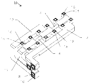
Figures 1 and 2 are isometric views of conductor matrices comprising
pluralities of conjoined conductors according to the disclosure.
Figure 3 is an isometric view of an electrical component comprising
installed conductors manufactured in accordance with the disclosure.
DETAILED DESCRIPTION OF THE PREFERRED EMBODIMENTS
Figures 1 and 2 illustrate cast conductor matrices, generally shown at 10,
according to the disclosure. Conductor matrices 10 each comprise a plurality
of
commonly-cast electrical conductors 12 conjoined by at least one temporary
link, or
frangible portion, 14. Conductors 12 comprise a plurality of contact faces 16.
Mounting holes 18 may be disposed in or through one or more of contact faces
16.
Contact faces 16 may be intended to provide sure and efficient electrical
contact between conductors 12 and other conductors 12 and/or other electrical
contacts, including contacts for, for example, electrical devices such as
MOSFET
transitors. At least some or all of contact faces 16 may be commonly-oriented.
To
say that contact faces 16 are commonly oriented means that, to the extent such
faces
are planar, they lie in substantially parallel planes (that is, they are
substantially co-
planar); or, to the extent that they are not planar, axes drawn normal from
their most
prominent points are substantially parallel. As will be understood by those
skilled in
the relevant arts, terms such as `substantially parallel' or `substantially co-
planar'
mean parallel or co-planar within normal manufacturing tolerances or
expectations.
Figure 3 illustrates an electrical component such as a bus structure or other
assembly, generally shown at 20, that may be produced using, for example,
-2-
CA 02723990 2010-12-06
conductors 12 of the conductor matrix 10 of Figure 2. Electrical bus structure
20
comprises the conductors 12 that are connected between respective electrical
components 22. In addition to providing electrical connections between their
respective electrical components 22, conductors 12 may also serve as part of
or the
entirety of the structural framework for the electrical bus structure 20, so
that
conductors 12 may provide desired spatial orientation and structural support
for
components 22 subject to gravity, magnetic forces, buffets, accelerations, or
other
potentially displacing loads. Electrical components 22 may include any
suitable or
otherwise desired electrical components, including for example MOSFET
transistors;
capacitors; controllers; pressure, temperature, or other transducers; data
processing or
communications components; transformers, thermostats, rheostats, etc.
Among the advantages offered by methods and devices disclosed herein are
improved efficiencies and cost savings provided by common casting, machining,
and
finishing processes, which can be applied to multiple conductors
simultaneously,
particularly where relevant portions of conductors 12, including for example
contact
faces 16, are co-planar and/or otherwise commonly oriented.
Methods for producing pluralities of conductors 12 according to the
disclosure may include, for example: casting a conductor matrix 10 of
conjoined
conductors 12; finishing at least a portion of the conductor matrix 10
corresponding
to the contact face 16 of at least one of the conductors 12; and separating
the
conductors 12 from each other by, for example, severing, flexing, or otherwise
breaking one or more frangible portions 14. A suitable surface treatment may
be
applied to at least a portion of the conductor matrix 10.
Conductor matrices 10 may be cast in accordance with the disclosure by any
known or otherwise suitable processes, including for example hereafter-
developed
processes and the process of investment casting (such as lost-wax) where a
ceramic
or other suitable mold (not shown) is produced from a disposable pattern (not
shown)
and the conductor matrix 10 is subsequently cast in the mold. Such a pattern
may
represent a 3-dimensional model of the conductor matrix 10. The pattern may be
designed using any suitable process, including for example suitably-
implemented
conventional computer aided design (CAD) systems. The pattern may be then
-3-
CA 02723990 2010-12-06
produced from wax using conventional methods or from a resin using a rapid
prototyping system. For example, the pattern may be produced using
stereolithography (SLA) and removed from the mold by burning. The conductor
matrix 10 may be cast using materials suitable for use as electrical
conductors such
as, for example, copper, aluminum, copper alloys and aluminum alloys. Casting
of
the conductors 12 provides the designer with the freedom to design the shape
and
configuration of the conductors 12, including the orientation of contact
surfaces 16,
based on factors such as desired current flow, heat dissipation and
assembly/packaging requirements of the electrical assembly 20. For example, as
will
be understood by those skilled in the relevant arts, it may be desirable to
produce
conductors have a varying cross-section and/or sharp or gradual corners.
Molds for conductor matrices 10 may be designed so as to facilitate casting
processes and subsequent operations required to manufacture conductors 12. In
order
to facilitate assembly and reduce assembly times, a conductor matrix 10 may
optionally be cast in the same (exact or modified) configuration and relative
positioning of the conductors as they are intended to be assembled into the
bus or
other electrical assembly 20 (see Figures 2 and 3).
Links or frangible portions 14 may be provided in order to allow for several
conductors to be cast together in a single step by permitting the molten
material to
flow in the mold and form both all of the conductors 12 in the conductor
matrix 10
and optionally the frangible portions 14 as well. The number of links 14 and
the
configuration (size, shape, positioning) of the links 14 may be determined
using
conventional, new, modified, or otherwise desired mold design techniques. In
some
circumstances, as will be understood by those skilled in the relevant arts,
conductor
matrix 10 may advantageously be cast to as close to the final dimensions as
possible.
In the same or other circumstances it may also be advantageous (e.g.,
practical and
economical) to add features to the conductor matrix 10 using one or more
subsequent
finishing operations.
For example, finishing of one or more contact faces 16 may be required or
desired to produce suitable surface properties for electrically and/or
structurally
connecting the conductors 12 to respective components. Finishing operations
used to
-4-
CA 02723990 2010-12-06
produce contact faces 16 may include suitable material removal processes such
as
machining and/or grinding. Subsequent drilling or finishing of the mounting
holes 18
may also be required or desired.
Conductors 12 may be positioned in the conductor matrix 10 so as to
facilitate any subsequent finishing operations. For example, the conductors 12
may be
positioned to orient the contact faces 16 in a common orientation if possible,
or at
least in a reduced number of orientations. As previously noted, commonly-
oriented
faces may, for example, have normals that are substantially parallel or may
include
cylindrical surfaces having central axes that are substantially parallel. The
term
"commonly oriented" may be used to describe surfaces that are oriented so that
they
can be finished in a single setup on a finishing machine. For example, the
commonly-
oriented contact faces 16 in Figure 1 may be machined in a single setup while
the
conductor matrix 10 is positioned and clamped on a bed of a machine tool,
without
requiring re-positioning and re-clamping of the conductor matrix 10 on the
machine
tool bed. Accordingly, the conductor matrix 10, including contact faces 16,
may be
configured so as to reduce the number of setups in a finishing machine.
Contrary to
conventional methods where conductors are manufactured individually, the above
method allows for multiple conductors 12 to be cast together and also finished
together in a reduced number of operations and at a reduced cost.
Conjoined conductors 12 may be separated from each other at any
convenient time. For example, conjoined conductors 12 may be separated from
each
other during finishing processes or during assembly of the electrical bus
structure or
other electrical assembly 20. If the electrical components 22 can be assembled
directly to the cast conductor matrix 10, the conjoined conductors 12 may
alternatively be separated after assembly by cutting the links 14 using a
suitable tool.
Advantageously, the conductors 12 may be separated once any finishing
operation
has been fully or partially completed. The conductors 12 may then be connected
to
their corresponding electrical components 22 in order to form, for example,
the
electrical bus structure 20 shown in Figure 3. The conductors 12 may be
separated
from each other by breaking the links 14. Depending on the configuration and
-5-
CA 02723990 2010-12-06
properties of the links 14, the links 14 may be broken or cut using a suitable
tool such
as a saw or grinder.
One or more surface treatments to enhance the properties such as the
corrosion resistance, surface hardness, or conductivity of conductors 12 may
optionally be applied to at least a portion of the conductor matrix 10.
Suitable surface
treatments may include, for example, anodization, powder or other coating or
plating
processes. The surface treatment may optionally be applied to the entire
conductor
matrix 10 prior to the finishing of the contact faces 16. Alternatively, the
surface
treatment may be applied to regions of the conductor matrix 10 other than the
contact
faces 16.
Conductors 12 may be made of any suitable material that may be cast and
also be used as an electrical conductor. Conductors 12 may have any desired or
required configuration(s), including for example complex geometric
configurations
of varying cross-section, so as to optimize their electrical and/or their
structural
properties. Accordingly, for example, inductive components or coils (not
shown) may
be formed as part of the electrical and/or structural framework of an
electrical bus
structure.
While the invention has been described and illustrated in connection with
specific, presently-preferred embodiments, many variations and modifications
may be
made without departing from the spirit and scope of the invention. The
invention is
therefore not to be limited to the exact components or details of methodology
or
construction set forth above. Except to the extent necessary or inherent in
the
processes themselves, no particular order to steps or stages of methods or
processes
described in this disclosure, including the Figures, is intended or implied.
In many
cases the order of process steps may be varied without changing the purpose,
effect,
or import of the methods described. The scope of the claims is to be defined
solely
by the appended claims, giving due consideration to the doctrine of
equivalents and
related doctrines.
-6-