Note: Descriptions are shown in the official language in which they were submitted.
CA 02724614 2010-11-16
WO 2009/138569 PCT/F12009/050396
A SENSOR FOR DETECTION OF CONDUCTIVE BODIES
The present invention relates to capacitive detection of conductive bodies or
targets, e.g. human beings.
BACKGROUND
Presence of bodies or objects may be detected by determining a change of
capacitance between two plates. The presence of an object causes a
change in the dielectric constant between the plates, which causes a
change in the capacitance formed by said two plates.
A capacitive sensor may be used e.g. to detect movements of people e.g. in
an anti-theft alarm system.
SUMMARY
An object of the present invention is to provide a sensor, a system, and a
method for detection of conductive bodies.
The sensor comprises at least a first signal electrode, a second signal
electrode, and a base electrode, which have been disposed in or on an
electrically insulating substantially planar substrate. The base electrode is
between the signal electrodes, wherein the distance between the first signal
electrode and the second signal electrode is smaller than or equal to 20% of
the width of the signal electrodes.
The sensor according to the invention may provide improved sensitivity
when compared to a conventional sensor where the width of the signal
electrode is substantially equal to the width of a ground electrode or when
difference in the widths of the electrodes is smaller than according to the
present invention.
The sensor according to the invention may detect the presence of
conductive bodies which are farther away from the sensor than in case of
conventional sensor where the width of the signal electrode is substantially
CA 02724614 2010-11-16
WO 2009/138569 PCT/F12009/050396
2
equal to the width of a ground electrode. The sensor according to the
invention has an extended reading distance for conductive objects.
The sensor according to the invention may be substantially insensitive to the
alignment of the detectable body. The inactive area between the signal
electrodes is small, and consequently it is virtually impossible to e.g. step
on
said inactive area. Blind spots may be avoided. The orientation of e.g. a foot
of a person does not have a significant effect on the detectability.
The embodiments of the invention and their benefits will become more
apparent to a person skilled in the art through the description and examples
given herein below, and also through the appended claims.
BRIEF DESCRIPTION OF THE DRAWINGS
In the following examples, the embodiments of the invention will be
described in more detail with reference to the appended drawings, in which
Fig. 1 shows a sensor in a three dimensional view,
Fig. 2 shows, in a three dimensional view, a person stepping on a
sensor,
Fig. 3 shows, in a side view, a person's foot positioned over a signal
electrode,
Fig. 4 shows, in a side view, a person's foot positioned over a signal
and a base electrode,
Fig. 5 shows, in a side view, a person's foot positioned over a sensor
according to prior art,
Fig. 6 shows an equivalent circuit of a system comprising a sensor and
a body,
Fig. 7a shows an equivalent circuit of a sensor without the presence of a
body,
CA 02724614 2010-11-16
WO 2009/138569 PCT/F12009/050396
3
Fig. 7b shows an equivalent circuit of a system comprising a sensor, a
body, and ground,
Fig. 8a shows an equivalent circuit of a system comprising a sensor and
a cover layer disposed over the sensor,
Fig. 8b shows an equivalent circuit of a system comprising a sensor, a
body, and a cover layer between the sensor and the body.
Fig. 9a shows signal and base electrodes disposed over a substrate,
Fig. 9b shows signal and base electrodes disposed under a substrate,
Fig. 9c shows signal and base electrodes between two substrates,
Fig. 9d shows signal and base electrodes disposed on different sides of
a substrate,
Fig. 10 shows a sensor comprising an array of substantially rectangular
signal electrodes having a base electrode structure between
them,
Fig. 11 shows a sensor comprising an array of signal electrode groups,
wherein each group comprises several signal electrodes
connected in series,
Fig. 12 shows a base electrode structure which surrounds signal
electrodes only partially.
Fig. 13a shows a sensor comprising an array of triangular signal
electrodes,
Fig. 13b shows a sensor comprising an array of hexagonal signal
electrodes,
CA 02724614 2010-11-16
WO 2009/138569 PCT/F12009/050396
4
Fig. 13c shows a sensor an array of square signal electrodes having
rounded corners, and star-shaped base electrode areas in the
vicinity of the corners of the signal electrodes,
Fig. 14a shows a web comprising signal and base electrode structures,
Fig. 14b shows a sensor provided by cutting the web of Fig. 14a,
Fig. 15 shows a measuring system comprising an array of signal
electrodes and multiplexing unit,
Fig. 16 shows a measuring system comprising an array of signal
electrodes and an array of monitoring units, and
Fig. 17 shows a sensor comprising an array of substantially circular
signal electrodes,
All drawings are schematic.
DETAILED DESCRIPTION
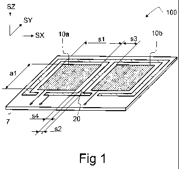
Referring to Fig. 1, a capacitive sensor 100 comprises a first signal
electrode 10a, a second signal electrode 10b, and a base electrode
structure 20 between said signal electrodes 10a, 10b. The base electrode
structure 20 is herein called as a base electrode 20.
The electrodes 1 Oa, 1 Ob, 20 have been implemented in or on an electrically
insulating substantially planar substrate 7. The sensor 100 may comprise
e.g. metal foils 10a, 10b, 20 attached to a plastic foil 7. The sensor 100 may
be flexible to facilitate transportation and storage in rolls. The thickness
of
the sensor (in direction SZ) may be smaller than or equal to 1 mm.
SX, SY and SZ denote three orthogonal directions. The directions SZ and
SY define the plane of the substrate 7.
CA 02724614 2010-11-16
WO 2009/138569 PCT/F12009/050396
al denotes the height of the signal electrode 10a (in direction SY). s1
denotes the width of the signal electrode 10a (in direction SX). s3 denotes
the distance between the first signal electrode 10a and the second signal
electrode 10b. s2 denotes the width of that part of the base electrode 20
5 which is between the signal electrodes 10a, 10b. s4 denotes the width of a
gap between the signal electrode 10a and the base electrode 20.
The distance s3 between the first signal electrode 10a and the second
signal electrode 10b may be e.g. in the range of 5 to 30 mm.
The width s2 may be e.g. in the range of 0.3 to 15 mm, advantageously in
the range of 1 to 7 mm, preferably in the range of 2 to 7 mm. The width s4
may be e.g. in the range of 0.3 to 15 mm, advantageously in the range of 1
to 7 mm.
The widths s2 and s4 may be substantially equal.
The surface area of the second signal electrode 10b may be in the range of
70% to 150% of the surface area of the first signal electrode 10b.
The surface area of the first signal electrode may be in the range of 0.02 to
0.2 m2 to match e.g. with size of a foot of a person.
The presence of a body in the vicinity of the sensor is detected by
monitoring a change in the capacitance of the first signal electrode 10a and
the base electrode 20 by a monitoring unit 50 (see Figs. 3 and 7b).
The presence of a body is detected by varying the voltage of a signal
electrode with respect to the base electrode, and by determining a value
which depends on the current of said signal electrode caused by said
voltage variations. For example, a signal electrode may be charged to a
predetermined voltage value, and discharged via a resistor to the base
electrode. The presence of an object may be detected based on the time
constant of the voltage decay. The voltage all signal electrodes may be
varied with a substantially similar waveform.
CA 02724614 2010-11-16
WO 2009/138569 PCT/F12009/050396
6
The base electrode 20 acts as a counter-electrode for capacitive
measurement. In addition, the base electrode 20 acts as a noise shield, i.e.
as a Faraday cage.
In addition, also a change in the capacitance of the second signal electrode
1 Oa and the base electrode 20 may be detected by a monitoring unit 50.
Base electrodes 20, which at least partially surround each of the signal
electrodes 10a, 10b individually, may be in contact with each other. Thus, a
single base electrode structure 20 may surround the first 10a and the
second 1 Ob signal electrode.
Fig. 2 shows a person walking over a sensor 100, which comprises several
independent signal electrodes 1Oal, 10a2, 1Ob1, 10b2, 10c1, 10c2, and one
or more base electrodes 20.
The voltage of the signal electrode 10b1 is varied with respect to the base
electrode 20 and the ground GND. The varying voltage of the signal
electrode is capacitively coupled via the foot of the person to the body
BOD1 of the person. The voltage is varied at such a frequency that the body
BOD1 acts as an electrical conductor. Consequently, the whole body BOD1
of the person has a varying (e.g. alternating) voltage VHG with respect to the
base electrode 20 and the ground GND. This causes a varying electric field
E between the body BOD1 and the base electrode 20, as well as between
the body BOD1 and the ground GND. Thus, the person's body is effectively
coupled as a part of a capacitive system formed by the electrodes 10b1, 20,
and the ground GND.
The capacitance of each signal electrodes 10al, 10a2, 10b1, 10b2, 10c1,
10c2 with respect to the base electrode may be monitored substantially
independently. Thus, the location of the person may be effectively tracked.
For optimum spatial resolution, the area of an individual signal electrode
may be in the range of 0.02 m2 to 0.2 m2, i.e. comparable to the bottom are
of the foot H1.
There may be cover layer 120 between the sensor 100 and the body BOD1.
The cover layer may be e.g. a carpet or a layer of epoxy coating. dl
CA 02724614 2010-11-16
WO 2009/138569 PCT/F12009/050396
7
denotes the thickness of the cover layer 120. The thickness d1 of the cover
layer may be e.g. in the range of 2 to 10 mm.
Fig. 3 shows a side view of a person's foot stepping over a signal electrode
10a. A monitoring unit 50 varies the voltage V12 of the signal electrode 10a
with respect to the base electrode 20 and the ground GND.
The measuring system 200 comprises the sensor 100 and a monitoring unit
50.
The ground GND may also act as an electrode 800 having a very large
area.
The width s1 of the signal electrodes 10a, 10b may be selected to be e.g. in
the range of 0.5 to 2 times the length SH (Fig. 4) of the foot H1. In order to
provide optimum spatial resolution. The narrow distance s3 between the
signal electrodes 10a, 10b makes it nearly impossible to step onto an
inactive grounded area, where the presence of the person would not be
detected.
The monitoring unit 50 provides a varying voltage V12 at least to the
electrodes 10a, 20, and it determines a value which depends on the current
of said signal electrode caused by said voltage variations. The monitoring
unit 50 may comprise a decision sub-unit (not shown) for generating a digital
signal based on said value or based on the rate of change of said value.
The digital signal may indicate the presence or absence of the body BOD1
in the vicinity of the electrode 10a.
The voltage V12 coupled to the signal electrode 10a may vary at a frequency
f1 which is e.g. in the range of 20kHz to 1 MHz, advantageously in the
range of 50 kHz to 300 kHz. The voltage V12 may have a complex
waveform, and in that case at least 90% of the power of the spectral
components of said varying voltage (V12) may be within the frequency range
of 20kHz to 1 MHz, preferably within 50 kHz to 300 kHz
The use of a higher frequency f1 may lead to increased power consumption.
The conductivity of e.g. human body may decreases at high frequencies.
The signal-to-noise ratio may be low at a lower operating frequency f1. The
CA 02724614 2010-11-16
WO 2009/138569 PCT/F12009/050396
8
frequency f1 may be selected so that the sensor 100 does not generate
interference to other electric devices, e.g. to medical appliances.
Fig. 4 shows the foot H1 of the person stepping over the base electrode 20.
The capacitance of a capacitor formed between the foot H1 and the base
electrode is substantially smaller than the capacitance of a capacitor formed
between the foot H1 and the signal electrode, because the width s2 of the
base electrode 20 is substantially smaller than the width s1 of the signal
electrode 10a (see Fig. 1). Consequently, the voltage VHG coupled to body
BOD1 may have nearly the same magnitude as the voltage V12 provided by
the monitoring unit 50.
The second signal electrode 10b may be switched to a high-impedance
floating state when the varying voltage V12 is coupled to the first signal
electrode 10a. Thus, the second signal electrode 10b does not capacitively
short-circuit the voltage VHG coupled to the body BOD1, and a coupled
voltage VHG may be high although the foot H1 is partially over the second
signal electrode 10b, in addition to being over the first signal electrode 10a
and over the base electrode 20.
A single monitoring unit 50 may be connected to the first and to the second
signal electrode by time-based multiplexing, by using a multiplexing unit 55
(Fig. 15). The multiplexing unit 55 may be arranged to disconnect the
second signal electrode 10b from the monitoring unit 50 and to leave it in a
high impedance state when the varying voltage V12 is coupled to the first
signal electrode 10a.
In particular, substantially all signal electrodes adjacent to the first
signal
electrode 10a, may be switched into the high impedance state when the
detection is performed by using the first signal electrode 10a.
Alternatively, varying voltages V12 may be simultaneously connected to the
first signal electrode 10a and to the second signal electrode 10b. The
varying voltages V12 coupled to the first signal electrode 10a and to the
second signal electrode 10b may be substantially in the same phase In
order to provide a high coupled voltage VHG also in a situation when the foot
H1 is partially over the second signal electrode 10b, in addition to the first
signal electrode 10a and the base electrode 20. However, the spatial
CA 02724614 2010-11-16
WO 2009/138569 PCT/F12009/050396
9
resolution may be worse than when switching the second signal electrode
into the high-impedance state.
Fig. 5 shows a comparative example (Prior Art), where the width s2 of a
base electrode 20 is substantially equal to the width of the signal electrode
10a. In that case the voltage VHG coupled to the body BOD1 is nearly 50%
lower than in case of Figs 3 and 4, because, and the capacitance between
the foot H1 and the base electrode 20 is substantially equal to the
capacitance between the foot H1 and the signal electrode 10a. The foot H1
is partially short circuited to the base electrode 20 due to the large area of
the base electrode 20.
The voltage VHG coupled to the body BOD1 in case of Figs. 3 and 4 is
approximately 50-100% higher than in case of Fig. 5. Thanks to the large
signal electrode 10a, the body BODI is effectively coupled to it. Simulations
and experimental measurements indicate a signal to noise ratio (S/N) which
is increased by 50% to 100% when compared to the situation of Fig. 5. The
improved signal to noise ratio enables a more sensitive measurement
and/or a longer reading distance.
The sensor according to Fig. 5 does not utilize effectively the electrical
conductivity of the body BOD1. It merely detects a change of permittivity
caused by the presence of the foot H1. This leads to a limited detection
performance when compared with the present invention.
The sensor 100 of Figs. 3 and 4 according to the present invention is
optimized for detecting the presence of conductive bodies BOD1 which
substantially extend from the level of the substrate, e.g. upwards.
The sensor 100 according to Figs 3 and 4 take advantage of the electrical
conductivity of the body BOD1, thus providing improved sensitivity when
compared with the prior art solutions (Fig. 5). Almost the whole surface area
of the body BOD1 is coupled act as a capacitive electrode (not the bottom
area of the foot 1-11) which creates an electric field E together with the
base
electrode 20 and possibly also with the earth GND, 800.
The sensor 100 is optimized to detect the presence of large conductive
objects. A conductive object may be considered to be a "large" if its vertical
CA 02724614 2010-11-16
WO 2009/138569 PCT/F12009/050396
dimension z1 (in the direction SZ) is greater than the dimension al and the
dimension s1 of the signal electrode 10a (Fig. 1).
The sensor 100 has a reduced sensitivity for smaller objects which are
5 positioned at a low level. This is an advantage when the aim is e.g. to
distinguish the presence of a human being from the presence of a smaller
non-conductive object such as a wooden chair, for example.
For example, it was experimentally noticed that a glass of water positioned
10 on the signal electrode 10a provided a rather low signal, wherein the
signal
level increased drastically when a person toughed the water in the glass
with his finger.
For conventional sensors having signal and ground electrodes of equal size
(Fig. 5), and having the gap width between said electrodes substantially
equal to size of said electrodes, it has been noticed that the effective
reading distance of such sensors is approximately only 1.33 times the gap
between the electrodes. Thus, for the sensor 100 according to the present
invention, the sensitivity for low objects may be reduced by selecting the
gap width s4 between the signal electrode 10 and the base electrode 20 to
be smaller than the thickness d1 of the cover layer 120. The gap width s4
advantageously smaller than 0.75 times the thickness d1 of the cover layer.
Fig. 6 shows a simplified equivalent circuit of system comprising a sensor
100 and a body BOD1. A varying voltage V12 is coupled between terminals
T1 and T2. The terminal T2 is coupled to a signal electrode 10 and the
terminal T1 is coupled to a base electrode 20. The signal electrode 10 and
the base electrode 20 form a capacitor CVG1 even when a body BOD1 is not
present.
When a body BODI is positioned in the vicinity of the electrodes 10a, 20, an
impedance ZH formed by the body is capasitively coupled between the
electrodes 10, 20. The body BODI and the signal electrode 10 form
together a capacitor CVH. The body BOD1 and the base electrode 20 form
together a capacitor CHG1.
Fig. 7a shows a more detailed equivalent circuit of a measuring system
where the base electrode 20 is also connected via a terminal TO to the
CA 02724614 2010-11-16
WO 2009/138569 PCT/F12009/050396
11
ground GND. The ground GND forms an additional, very large capacitor
plate 800. The signal electrode 10 and the ground GND form together a
further capacitor CVG2, even when a body BND is not present.
The base electrode may be connected to the ground, e.g. to the ground of
the mains network in a building, to the metallic water pipelines of a building
or to a special ground electrode buried into the soil. This helps to provide a
very large electrode surface. Alternatively, or in addition to, the ground GND
may also be established by those parts of the base electrode structure
which are relatively far away from the body BOD1 or which are far away
from the foot H1 of a person. The base electrode may be mesh structure
which covers substantially the entire area of a room. Thus, it may represent
a relatively large surface area.
The surface area of the base electrode structure 20 may be greater than or
equal to the surface area of the first signal electrode 1 Oa.
Referring to Fig. 7b, the surface of an electrically conductive body BOD1
has surfaces H1, H2 and H3, by which the impedance ZH of the body BOD1
is capacitively coupled to the signal electrode 10, to the base electrode 20,
and to the ground GND. The body BODI forms a capacitor CVH together
with the signal electrode 10. The body BOD1 forms a capacitor CHG1
together with those parts of the base electrode 20 which are in the vicinity
of
the body BOD1. The body BOD1 forms a capacitor CHG2 together with the
ground GND, 800.
Referring to Figs 8a and 8b, a cover layer 120 may be positioned over the
electrodes 10, 20. Fig. 8a shows the equivalent circuit without the presence
of a body BOD1, and Fig. 8b shows the equivalent circuit with the
impedance ZH of the body. The dielectric permittivity of the cover layer 120
deviates from the permittivity of air. Thus, the capacitance of the capacitors
CVG1, CVH9 CHG1, CHG2 is different from the values of Figs. 8a and 8b.
Fig. 9a shows a sensor wherein the signal electrodes 1 Oa, 1 Ob and the base
electrode have been implemented on an electrically insulating substrate 7
substantially in the same plane.
CA 02724614 2010-11-16
WO 2009/138569 PCT/F12009/050396
12
Fig. 9b shows the sensor 100 of Fig. 9a upside down. Now the substrate 7
protects the electrodes from wear and prevents a galvanic contact between
the electrodes and conductive bodies BOD1. However, the surface below
the sensor 100 should be electrically insulating. The sensor 100 may be e.g.
glued into a floor. In that case the glue and the floor should be electrically
insulating.
Fig. 9c shows a sensor 100 where the signal electrodes 10a, 10b and the
base electrode 20 have been implemented between two substrates 7a, 7b.
In that case the electrodes 1 Oa, 1 Ob, 20 are well protected from both sides.
Fig. 9d shows a sensor where the signal electrodes 10a, 10b are at a
different level than the base electrode 20. This may be more complex to
manufacture than the examples shown in Figs. 9a to 9c.
The upper and/or lower side of sensor 100 may be coated with an adhesive
(not shown) in order to facilitate easier installation e.g. on a floor. E.g. a
pressure sensitive adhesive (pressure-activated adhesive) may be used.
The adhesive layer may be protected by a removable release layer (not
shown). Installation is also possible by using normal gluing methods known
in the art.
Referring to Fig. 10, the sensor 100 may comprise an array of substantially
rectangular signal electrodes 10, which have at least one base electrode
structure 20 between them.
Referring to Fig. 11, two or more signal electrodes may be coupled
electrically in series and/or in parallel in order to increase an individually
monitored area.
Referring to Fig. 12, at least 70% of the perimeter of a signal electrode 10a
may be surrounded by the base electrode 20. Advantageously, at least 95%
of the perimeter of the signal electrode 1 Ob may be surrounded by the base
electrode 20 as shown also in Figs. 11 and 14b. The base electrode 20 may
also completely surround the signal electrode, as shown e.g. in Fig. 10.
Referring to Fig. 13a, the sensor 100 may comprise a substantially
triangular array of signal electrodes 10.
CA 02724614 2010-11-16
WO 2009/138569 PCT/F12009/050396
13
Referring to Fig. 13b, the sensor 100 may comprise a substantially
hexagonal array of signal electrodes 10.
Referring to Fig. 13c, the sensor 100 may comprise e.g. rectangular signal
electrodes 10 having rounded corners. The base electrode 20 may have
star-shaped areas.
The sensors 100 of Figs 10, 13a or 13b may comprise electrical
feedthroughs (vias) in order to couple connectors to the signal electrodes
which are in the middle of the array. The sensors 100 of Figs 10, 13a or 13b
may also be modified in a similar way as in Fig. 11 so as to implement the
conductive parts in a single plane.
The signal electrodes 10 may also have other forms, e.g. octagonal or
circular shape. Adjacent signal electrodes may have a different shape.
However, it is advantageous to select the shape(s) of the signal electrodes
10 such that the distance between adjacent signal electrodes is kept
substantially at the predetermined value s3 (Fig. 1). Thus, the signal
electrodes may have mutually matching contours.
Referring to Fig. 14a, a plurality of signal electrodes 10 and at least one
base electrode structure 20 may be implemented on a sensor web 77, e.g.
on a continuous band comprising electrode structures. A substantially
similar electrode pattern may be periodically copied along the web in the
direction SX, i.e. in the longitudinal direction of the web 77. The electrode
pattern has a period, which has a length LI.Thus, the consecutive periods
PRDk+o, PRDk+l, PRDk+2, PRDk+3, PRDk+4 have substantially the same
electrode pattern and substantially the same length L1. In other words, the
web 77 may exhibit periodicity.
The signal electrodes 10 of successive periods may be electrically isolated
from each other. Each of the electrodes 10, 20 is connected to a conductor
W. The conductors W of at least three periods may be arranged to cross a
transverse line LIN2, wherein conductors from farther periods may be
arranged to terminate without crossing the line LIN2.
CA 02724614 2010-11-16
WO 2009/138569 PCT/F12009/050396
14
The electrodes and the conductors are advantageously implemented in the
same plane in order to simplify the manufacturing of the web 77.
The web 77 may manufactured e.g. by using a roll-to-roll process.
The sensor 100 shown in Fig. 14b may be obtained by cutting along the
lines LIN1, LIN2 of the continuous web 77 of Fig. 14a. The conductors Wal,
Wa2, Wa3, Wb1, Wb2, Wb3, Wcl, Wc2, Wc3, and Wd3 terminate in the
vicinity of the cut edge of the sensor 100. This facilitates coupling of a
connector CONI to said conductors, in order to individually monitor the
presence of objects in the vicinity of the signal electrodes 10al, 10a2, 10b1,
10b2, 10c1, 10c2. The base electrodes 20a3, 20b3 and 20c3 are shown to
be connected together. However, they may also be galvanically separate.
The sensor comprises conductors Wdl, Wd2, We3, which terminate before
reaching said cut edge. These conductors were connected to electrodes,
which were cut away from the sensor 100, or which will be inactive.
Referring to Fig. 15, the measuring system 200 may comprise the sensor
100, a multiplexing unit 55, a monitoring unit 50, and a data processor 60.
The multiplexing unit 55 may be arranged to couple each independent
signal electrode 1Oa, 1Ob, 1Oc, 1 Od, 1 Of, 1Oe to the monitoring unit 50,
each
at a time. The multiplexing unit 55 may be arranged may be arranged to
switch all other signal electrodes to the high impedance state.
The data processor 60 be arranged to provide information on the location of
a body BOD1 based on signal or signals provided by said monitoring unit.
The system 200 may provide information on the movement of the body
BOD1 based on said signal or signals.
The data processor 60 may also communicate with the multiplexing unit 55
so as to control the order and/or the rate in which the varying voltage V12 is
coupled to the different signal electrodes. The multiplexing unit 55 may be
arranged to send a synchronization signal and/or information regarding the
identity of the electrode(s) which are activated at a given time.
Referring to Fig. 16, the measuring system 200 may comprise the sensor
100, one or more measuring units 50a, 50b, 50c, 50d, 50e, 50f, and a data
CA 02724614 2010-11-16
WO 2009/138569 PCT/F12009/050396
processor 60. Each independent signal electrode 10a, 10b, 10c, 10d, 10f,
10e may be connected to a respective monitoring unit.
The, the system 200 may comprise an array of monitoring units 50a, 50b,
5 50c, 50d, 50e, 50f coupled to an array of signal electrodes 10a, 10b, 10c,
10d, 10e, 10f, and a data processor 60 arranged to provide information on
the location of a body BOD1 based on a plurality of signals provided by said
monitoring units. The system 200 may provide information on the movement
of the body BOD1 based on said signals.
Yet, referring to Fig. 17, the sensor 100 may comprise e.g. an array of
substantially circular signal electrodes 10 having e.g. star-shaped base
electrode areas between them. In this example the distance s3 between the
diagonally adjacent signal electrodes is greater than 20% of the width s1 of
the signal electrodes. Thus, the blind spot between signal electrodes is
rather large. However, because the width s2 of the base electrode structure
between the signal electrodes is still smaller than or equal to 20%
(preferably smaller than or equal to 10%) of the width s1 of the signal
electrode 10, the varying voltage is still effectively coupled to the body
BOD1.
The surface area of that part of the base electrode structure 20 which is
between the adjacent first and second signal electrodes may be smaller
than 20% of the surface area of the first signal electrode, and preferably
smaller than or equal to 10% of the surface area of the first signal
electrode.
The terminals of the conductors W are formed by cutting the sensor web
across its longitudinal direction to a desired length, and thus the ends of
the
conductors are exposed and are ready for forming an electrical contact. The
attachment method of the sensor web in contact can be, but is not limited to,
crimp connector, spring connector, welded contact, soldered contact,
isotropic or anisotropic adhesive contact. However, a standard connector
used in common electronic applications (e.g. Crimpflex , Nicomatic SA,
France) can be attached to the ends of the conductors W.
The surface area of a conductor W connected to a signal electrode 10a,
10b, 20 may be smaller than 10% of the surface area of said electrode, in
CA 02724614 2010-11-16
WO 2009/138569 PCT/F12009/050396
16
order to guarantee spatial resolution and in order to minimize power
consumption.
The sensor 100 may comprise at least six electrically separate signal
electrodes, which together cover at least 70% of the surface area of the,
substrate 7.
The sensor 100 according to the invention may be used e.g. to monitor the
presence and/or movements of people in private houses, banks or factories
in order to implement an anti-theft alarm system. A network of sensors 100
may be used to monitor the presence and/or movements of people in
department stores e.g. in order to optimize layout of the shelves. The sensor
may be used e.g. in hospitals or old people's homes to detect patient activity
and their 'vital functions. The sensor may be used in prisons to monitor
forbidden areas. The sensor may be used for detecting movement of other
large conductive bodies, such as wheelchairs or aluminum ladders. The
sensor may be used for detecting movement of animals.
The sensor 100 may be installed e.g. on or in a floor structure.
The substrate 7 may comprise plastic material, or fibrous material in the
form of a nonwoven fabric, fabric, paper, or board. Suitable plastics are, for
example, plastics comprising polyethylene terephtalate (PET),
polypropylene (PP), or polyethylene (PE). The substrate is preferably
substantially flexible in order to conform to other surfaces on which it is
placed. Besides one layer structure, the substrate can comprise more layers
attached to each other. The substrate may comprise layers that are
laminated to each other, extruded layers, coated or printed layers, or
mixtures of these. Usually, there is a protective layer on the surface of the
substrate so that the protective layer covers the electrically conductive
areas
and the conductors. The protective layer may consist of any flexible
material, for example paper, board, or plastic, such as PET, PP, or PE. The
protective layer may be in the form of a nonwoven, a fabric, or a foil. A
protective dielectric coating, for example an acrylic based coating, is
possible.
The electrically conductive areas comprise electrically conductive material,
and the electrically conductive areas can be, for example, but are not limited
CA 02724614 2010-11-16
WO 2009/138569 PCT/F12009/050396
17
to, printed layers, coated layers, evaporated layers, electrodeposited layers,
sputtered layers, laminated foils, etched layers, foils or fibrous layers. The
electrically conductive area may comprise conductive carbon, metallic
layers, metallic particles, or fibers, or electrically conductive polymers,
such
as polyacetylene, polyaniline, or polypyrrole. Metals that are used for
forming the electrically conductive areas include for example aluminum,
copper and silver. Electrically conductive carbon may be mixed in a medium
in order to manufacture an ink or a coating. When a transparent sensor
product is desired, electrically conductive materials, such as ITO (indium tin
oxide), PEDOT (poly-(3,4-ethylenedioxythiophene)), or carbon nanotubes,
can be used. For example, carbon nanotubes can be used in coatings which
comprise the nanotubes and polymers. The same electrically conductive
materials also apply to the conductors. Suitable techniques for forming the
electrically conductive areas include, for example, etching or screen printing
(flat bed or rotation), gravure, offset, flexography, inkjet printing,
electrostatography, electroplating, and chemical plating.
E.g. the following manufacturing method may be used. A metal foil, such as
an aluminum foil, is laminated on a release web. The electrically conductive
areas and the conductors are die-cut off the metal foil, and the remaining
waste matrix is wound onto a roll. After that, a first protective film is
laminated on the electrically conductive areas and the conductors. Next, the
release web is removed and a backing film is laminated to replace the
release web.
Benefits of the above-mentioned manufacturing method include:
- the raw material is cheaper,
- the manufacturing method is cheaper compared to e.g. etching,
- the manufacturing method requires only one production line, and
- the resulting sensor web is thinner; the thickness of the sensor web may
be less than 50 pm.
Electrically conductive areas and conductors may be die-cut from a metal
foil, and they may be laminated between two substrates, i.e. between two
superimposed webs.
Electrically conductive areas and their conductors may be located in one
layer, and optional RF loops and their conductors may be located in another
CA 02724614 2010-11-16
WO 2009/138569 PCT/F12009/050396
18
layer. In principle, it is possible to use different techniques, e.g. etching,
printing, or die-cutting, in the same product. For example, the electrically
conductive areas may be die-cut from a metal foil, but their conductors may
be etched. The electrically conductive areas and their conductors may be
connected to each other through vias.
The monitoring unit 50 may be arranged to provide a signal which depends
on the capacitance formed by the electrodes 10a, 20. Said signal may be
provided e.g. by a time constant measurement, by measuring an impedance
by using the varying voltage V12, by connecting the electrodes as a part of a
tuned oscillation circuit, or by comparing said unknown capacitance of the
electrodes with a known capacitance.
The time constant may be determined e.g. by charging the capacitor formed
by the electrodes to a predetermined voltage, discharging said capacitor
through a known resistor or inductor, and by measuring the rate of decrease
of voltage of said capacitor.
The impedance may be measured by varying the voltage of said capacitor,
by measuring the respective the current, and by determining- the ratio of the
change of current to the change of voltage.
The unknown capacitance of said capacitor may be determined by coupling
them as a part of a resonating circuit comprising and inductance and said
capacitor.
The unknown capacitance of said capacitor may be determined by charging
or discharging the unknown capacitance by transferring a charge to it
several times by means of a known capacitor unit a predetermined voltage
is reached. The unknown capacitance may be determined based on the
number of charge transfer cycles needed to reach the predetermined
voltage.
EXAMPLES
1. A sensor (100) for detecting presence of conductive objects (BOD1) , said
sensor (100) comprising a first signal electrode (10a), a second signal
CA 02724614 2010-11-16
WO 2009/138569 PCT/F12009/050396
19
electrode (10b), and a base electrode structure (20) implemented in or on
an electrically insulating substrate (7), wherein the distance (s3) between
said first signal electrode (10a) and said second signal electrode (10b) is
smaller than or equal to 0.2 times the width (s1) of said first signal
electrode
(10a), and wherein at least a part of said base electrode structure (20) is
between said first signal electrode (10a) and said second signal electrode
(10b), and wherein said base electrode structure surrounds at least 70% of
the perimeter of said first signal electrode (10a).
2. A sensor (100) for detecting presence of conductive objects (BOD1) , said
sensor (100) comprising a first signal electrode (10a), a second signal
electrode (10b), and a base electrode structure (20) implemented in or on
an electrically insulating substrate (7), wherein the surface area of that
part
of said base electrode structure (20) which is between said first signal
electrode (10a) and said second signal electrode (10b) is smaller than or
equal to 20% of the area of said first signal electrode (10a), and wherein
said base electrode structure surrounds at least 70% of the perimeter of
said first signal electrode (10a).
3. The sensor (100) of example 1 or 2 wherein the surface area of said
second signal electrode (10b) is in the range of 70% to 150% of the surface
area of said first signal electrode (10b).
4. The sensor (100) according to any of the examples 1 to 3 wherein the
surface area of said first signal electrode is in the range of 0.02 to 0.2 m2.
5. The sensor (100) according to any of the examples I to 4 wherein the
distance (s3) between said first signal electrode (10a) and said second
signal electrode (I Ob) is in the range of 5 to 30 mm.
6. The sensor (100) according to any of the examples 1 to 5 wherein the
width (s2) of a part of said base electrode structure (20) between said signal
electrodes is in the range of 0.3 to 15 mm.
7. The sensor (100) according to any of the examples 1 to 6 wherein the
surface area of said base electrode structure (20) is greater than or equal to
the surface area of said first signal electrode (1 Oa).
CA 02724614 2010-11-16
WO 2009/138569 PCT/F12009/050396
8. The sensor (100) according to any of the examples 1 to 7 wherein said
signal electrodes (10a, 10b) and said base electrode structure (20) are
substantially in the same plane, and conductive parts of said sensor (100)
have been implemented on a flexible substrate (7).
5
9. A monitoring system for detecting a conductive body (BOD1), said system
comprising a sensor (100) according to any of the examples 1 to 7, said
system further comprising a monitoring unit (50), which is arranged to
couple a varying voltage (V12) between said first signal electrode (10a) and
10 said base electrode structure (20), and which is arranged to provide a
value
which depends on the current of said signal electrode (10a) caused by said
voltage variations.
10. The system of example 9 wherein said signal electrodes (10a, 10b) are
15 covered with an electrically insulating layer (120), the thickness (d1) of
said
layer being greater than a gap (s4) between said first measuring electrode
(1 Oa) and said base electrode structure (20).
11. The system of example 9 or 10 wherein said sensor (100) has been
20 installed on a floor and covered with a cover layer (120), wherein the
thickness (dl) of the cover layer over the electrodes is greater than or equal
to a gap (s(4) between the first signal electrode and the base electrode
structure (20).
12. The system according to any of the examples 9 to 11 wherein said base
electrode structure (20) connected to the earth (GND, 800).
13. The system according to any of the examples 9 to 12 wherein at least
90% of the power of the spectral components of said varying voltage (V12) is
within the frequency range of 20kHz to 1 MHz.
14. The system according to any of the examples 9 to 13 wherein the
second signal electrode 10b is switched to a high impedance state when the
varying voltage (V12) is coupled to said first signal electrode (10a).
15. The system according to any of the examples 9 to 14 comprising an
array of monitoring units (50) coupled to an array of signal electrodes, and a
data processor arranged to provide information on the location of said body
CA 02724614 2010-11-16
WO 2009/138569 PCT/F12009/050396
21
(BOD1) based on a plurality of signals provided by said monitoring units
(50).
16. The system according to any of the examples 9 to 15 system comprising
an array of monitoring units (50) coupled to an array of signal electrodes,
and a data processor arranged to provide information on the movement of a
body (BOD1) based on a plurality of signals provided by said monitoring
units (50).
17. A method of detecting a conductive body (BOD1) by using a sensor
(100) according to any of the examples 1 to 8 or a system according to any
of the examples 9 to 16, said method comprising coupling a varying voltage
(V12) between said first signal electrode (10a) and said base electrode
structure (20), and determining a value which depends on the current of
said signal electrode (1 Oa) caused by said voltage variations.
18. The method of example 17 wherein the vertical dimension (z1) of said
body (BOD1) is greater than or equal to the height (al) and the width (s1) of
said first signal electrode (10a).
19. A sensor web (77) comprising a plurality of sensors (100) according to
any of the examples 1 to 8, wherein a substantially similar electrode pattern
has been copied along the longitudinal dimension (direction SX) of said web
(77) so that the electrode pattern has a longitudinal period.
20. The sensor web (77) of example 19 wherein conductors W of at least N
successive periods cross a transverse line LIN2, wherein at least one
conductor connected to a signal electrode which does not belong to said N
periods terminates without crossing said transverse LIN2, N being an
integer greater than or equal to three.
21. A sensor (100) obtainable by cutting the sensor web (77) of example 20
along two transverse lines (LIN1, LIN2).
22. The sensor (100) of example 21 wherein conductors (We3, Wdl, Wd2),
which terminate without crossing said line LIN1 are not connected to any
signal electrodes.
CA 02724614 2010-11-16
WO 2009/138569 PCT/F12009/050396
22
The word "comprising" is to be interpreted in the open-ended meaning, i.e. a
sensor which comprises a first electrode and a second electrode may also
comprise further electrodes and/or further parts.
For a person skilled in the art, it will be clear that modifications and
variations of the devices and the method according to the present invention
are perceivable. The particular embodiments and examples described
above with reference to the accompanying drawings are illustrative only and
not meant to limit the scope of the invention, which is defined by the
appended claims.