Note: Descriptions are shown in the official language in which they were submitted.
CA 02725084 2010-11-19
WO 2010/010352 PCT/GB2009/001826
Diamond material
The present invention relates to methods of synthesising diamond material and
synthetic
diamond material which may be produced by such methods. The synthetic diamond
material has a high chemical purity and a high isotopic purity and it
therefore ideal for
use as a host material for a quantum spin defect suitable for spintronic
applications.
Over the last 20 years there has been substantial interest in the use and
manipulation of
single photon sources for the two principal application areas of cryptography
and
quantum computing.
These application areas use a fundamental property which exists in nature on a
quantum
scale; until a measurement is made, a particle which has two or more available
spin
states has to be considered as a particle having a superposition of all these
spin states.
The spin state of a particle e.g. a photon, electron, atomic nucleus, atomic
defect, etc,
with discrete spin states can be manipulated using a number of methods and the
spin
state can be detected and/or controllably altered, using an energy source or
detector. An
electron, photon, atomic nucleus or atomic defect with discrete spin states is
analogous
to a "bit" in a traditional computer and is termed a "quantum bit" (or "qubit"
or "qbit").
However, due to the quantum nature of the spin states, a qubit can exist in
not just one of
two spin states, but also in a superposition of these spin states. It is this
superposition of
spin states which makes it possible for qubit based computers to compute
certain
problems at a much greater speed than is possible for classical computers, and
in
cryptography applications enable a sender to know for certain if a message has
been
delivered to a receiver without an eavesdropper also learning of the message's
contents.
The key elements required for quantum information processing are: low error
coding of
qubits onto individual quantum systems; storage of quantum information for
long times
compared to the gate times; and controllable two-qubit interactions forming
fast
quantum gates.
CA 02725084 2010-11-19
WO 2010/010352 PCT/GB2009/001826
2
A large number of materials and structures have been proposed for use as qubit
hosts
ranging from quantum dot semiconductors to super-cooled ion traps. The
alternatives to
date suffer the disadvantage of operation only being possible at cryogenic
temperatures
or having very short transverse relaxation lifetimes (referred to as "T2"). In
contrast, the
nitrogen-vacancy ("NV") defect in diamond can have a T2 that is sufficiently
long for its
use in a range of applications at room temperature (about 300 K). The NV
centre in
diamond can be used for qubit applications since it has discrete quantised
magnetic spin
states. The NV centre has been thoroughly characterized using techniques such
as
electron paramagnetic resonance (EPR), photoluminescence (PL), optical
absorption
spectroscopy and spectroscopy under uniaxial stress. In diamond the NV centre
has
been identified in both the neutral and negative charge states ("NV " and "NV"
respectively). The NV centre in its negative charge state (NV-) has a zero
phonon line
("ZPL") at 637 nm compared with 575 rim for an NV centre in the neutral state
(NV ).
One major problem in producing materials suitable for qubit applications is
preventing
the qubits from decohering, or at least lengthening the time a system takes to
decohere
(i.e. lengthening the "decoherence time"). Decoherence is commonly understood
to be
the process by which quantum becomes classical; the process by which the
determinism
of the macroscopic world arises out of the superpositions and entanglements
that
describe the quantum one. Decoherence times may be quantified and compared
using
the transverse relaxation time T2. T2 is terminology used in NMR (nuclear
magnetic
resonance) and MRI (magnetic resonance imaging) technology and is also known
as the
"dephasing time" or the "spin-spin relaxation time". Transverse relaxation
describes the
relaxation of an excited magnetic moment that is perpendicular to a main
magnetic field
applied to a material back to equilibrium, that is, parallel to the magnetic
field. A long
T2 time is desirable in applications such as quantum computing as it allows
more time
for the operation of an array of quantum gates and thus allows more complex
quantum
computations to be performed.
In a particular material, the decoherence time can be related to the specific
magnetic
moment being considered, for example in diamond, the magnetic moment
associated
with the nucleus of a 13C atom may have a different T2 compared with the
magnetic
moment of the electronic spin state of an NV- centre. Each of these magnetic
moments
CA 02725084 2010-11-19
WO 2010/010352 PCT/GB2009/001826
3
can be advantageously used in quantum applications, although in many respects
they
show different benefits and limitations in this type of application, and so it
is important
to be clear about which magnetic moment the T2 is being reported. In this
specification,
unless indicated otherwise, "T2" will refer to the decoherence time of the
electronic spin
state of the quantum spin defect, for example the NV- centre in diamond, and
other T2
values will be suitably qualified, e.g. "T2[13C]" will refer to the T2 time
for the 13C
nuclear magnetic moment.
In US 7,122,837, NV centres in diamond are created in a controlled manner. In
one
embodiment, a single crystal diamond is formed using a CVD process, and then
annealed to remove NV centres. A thin layer of single crystal diamond is then
formed
with a controlled number of NV centres. The NV centres form qubits for use in
electronic circuits. Masked and controlled ion implants, coupled with
annealing are used
in CVD-formed diamond to create structures for both optical applications and
nanoelectromechanical device formation. Waveguides may be formed optically
coupled
to the NV centres and further coupled to sources and detectors of light
to.interact with
the NV centres.
Kennedy and Linares (Phys. Stat. Sol. (b), 233 (2002), 416-426) disclose
diamond
containing NV centres with a T2 of 32 gs at temperatures from 1.5 to 100 K.
Gaebel et al., Nature Physics, 2, June 2006, 408-413, describes natural
abundance single
crystal diamond containing NV centres formed by ion implantation which shows a
Hahn
echo decay time (decoherence time T2) of 350 .ts from an individual defect.
The internal optical transitions within the NV- defect take typically about 10
ns. For a
viable quantum computing device the T2 time must be much greater than this to
enable
enough gate operations for error correction etc. Hence a T2 time of more than
about
500 lts (0.5 ms) offers a respectable number of gated operations, typically
about 5 x 10⁴,
before decoherence is lost.
A further important parameter for some applications is related to the temporal
spectral
stability of the optical transition which can be used to read/write
information from the
CA 02725084 2010-11-19
WO 2010/010352 PCT/GB2009/001826
4
NV qubit. This is especially important where entanglement is to be achieved
between
the photons emitted from the individual qubits. The frequency of these photons
must be
identical to ensure one of the conditions of indistinguishability needed for
quantum
entanglement.
On the basis of the above, it is clear that there is a need for host materials
for quantum
spin defects, wherein when incorporated into the material, the quantum spin
defects have
higher T2 times, at room temperature, than have been demonstrated currently.
In
addition, it would be desirable to provide these quantum spin defects in a
form and/or
location which is readily accessible for characterisation and "read out", as
required by
the end application. It is further desirable that the frequency of the optical
transition
used to read/write to such quantum spin defects is stable.
In this regard, the present inventors have found that by carefully controlling
the
conditions under which diamond material is prepared using chemical vapour
deposition
(CVD) methods, it is possible to provide diamond material which combines a
very high
chemical purity with a very high isotopic purity. In particular, it has been
found that by
controlling both the chemical purity and the isotopic purity of.the materials
used in the
CVD process, it is possible to obtain synthetic diamond material which is
particularly
suitable for use as a host for a quantum spin defect. Surprisingly, it has
been found that
where such materials are used as a host for quantum spin defects, long T2
times are
obtained at room temperature and the frequency of the optical transitions used
to
read/write to the devices are stable.
More specifically, the present invention provides a method of preparing a
diamond
material of high chemical purity and high isotopic purity comprising:
providing a diamond substrate having a surface which is substantially free of
crystal
defects;
providing a source gas mixture comprising high purity gases, wherein the
concentration of nitrogen in the source gas mixture is about 300 ppb or less;
providing a solid carbon source comprising 12C in an amount of at least about
99%
of the total C content of the source, wherein the solid carbon source has a
low
nitrogen impurity content;
CA 02725084 2010-11-19
WO 2010/010352 PCT/GB2009/001826
activating and/or dissociating at least a portion of the source gas mixture
and the
solid carbon source to form gaseous carbon species; and
allowing homoepitaxial diamond growth on the surface of the substrate.
5 In this regard, the present inventors have surprisingly found that by using
a solid carbon
source having a high isotopic purity, it is possible to significantly increase
both the
chemical purity and the isotopic purity of the diamond material produced.
The present invention further provides a method of preparing a diamond
material of high
chemical purity and high isotopic purity comprising:
providing a diamond substrate having a surface which is substantially free of
crystal
defects;
providing a source gas mixture comprising high purity gases and a carbon
source
gas, wherein the high purity gases contribute about 300 ppb or less to the
total
nitrogen levels in the source gas mixture and the carbon source gas comprises
12C in
an amount of at least 99% of the total C content of the carbon source gas and
contains nitrogen impurities in amount of about 20 ppm or less;
dissociating the source gas; and
allowing homoepitaxial diamond growth on the surface of said substrate,
wherein at
least one of the following conditions is satisfied:
(a) the temperature of the substrate is in the range from about 800 C to about
1000 C; and
(b) oxygen is added to the source gas mixture in an amount of between about
0.5% and about 5% by volume, measured as 02 equivalent, of the total
source gas mixture.
The methods of the present invention provide synthetic diamond material which
has a high
chemical purity and a high isotopic purity. In this regard, the present
invention further
provides synthetic diamond material obtainable by the methods as defined
herein.
In a further aspect, the present invention provides a layer of synthetic
diamond material,
wherein the diamond layer has a total nitrogen concentration of about 5 ppb or
less and a
total concentration of 13C of about 0.9% or less.
CA 02725084 2010-11-19
WO 2010/010352 PCT/GB2009/001826
6
The layer of synthetic diamond material of the present invention has very low
impurity
levels and very low associated point defect levels. In addition the layer of
synthetic
diamond material may have a low dislocation density, low strain, and vacancy
and self-
interstitial concentrations which are sufficiently close to thermodynamic
values
associated with the growth temperature that its optical absorption is
essentially that of a
perfect natural diamond lattice. As such, it cannot be further improved in
material which
is diamond.
As a consequence of its high chemical purity and high isotopic purity, the
synthetic
diamond material of the present invention is particularly suitable for use as
a host for a
quantum spin defect.
Thus, the present invention further provides a solid state system comprising a
host
material and a quantum spin defect, wherein the quantum spin defect has a T2
at room
temperature of about 500 ps or more.
In the solid state systems according to the present invention, the quantum
spin defect, for
example an NV defect, has a surprisingly long T2 value at room temperature
Where a quantum spin defect is present in a host material, in the end
application of the
material, the quantum spin defect will need to be characterised and read out.
In order for
the system which comprises the host material and the defect to be useful for
e.g. quantum
computing applications, it is necessary that the frequency of the optical
transition which is
used to characterise and read out a quantum spin defect has a high spectral
stability. This
ensures that one quantum spin defect cannot be distinguished from any other
quantum spin
defect. Surprisingly, where a quantum spin defect is introduced into the layer
of synthetic
diamond material of the present invention or the diamond material produced by
the
methods of the present invention, the quantum defect exhibits a particularly
stable optical
transition.
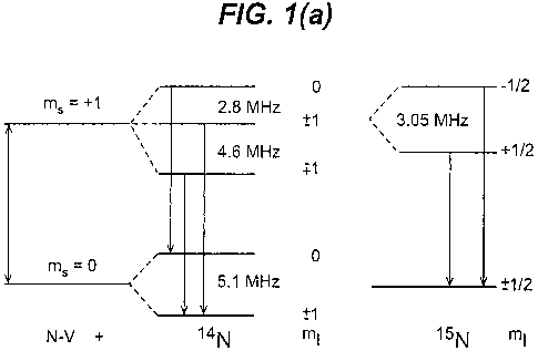
The spectral stability of a quantum spin defect, for example an NV centre in
the negative
charge state is quantified by the spread of frequencies of the photons emitted
by the centre
CA 02725084 2010-11-19
WO 2010/010352 PCT/GB2009/001826
7
over a time period, measured at room temperature (about 300 K). In the case of
an NV
centre in the negative charge state, the photon that is measured is the photon
that is emitted
when an electron in the ms = 1 excited state relaxes (i.e. de-excites) into
the ms = 0 ground
state. The photons associated with the zero phonon line (ZPL) have a nominal
wavelength
of 637 nm, corresponding to a frequency of approximately 4.7 x 10¹⁴ Hz (470
THz). By
determining the frequency of a large number of photons, a graph of number of
photons
having a particular frequency versus the frequency of the photon can be
plotted. Thus, the
synthetic diamond material layers of the present invention are suitable hosts
for quantum
spin defects.
By virtue of the techniques used to perform read out of a quantum spin defect,
and also the
method of its preparation, for example ion implantation techniques where it is
only possible
to introduce defects within a few microns of the surface, this
characterisation is normally
carried out on the region of the material within about 100 m of a surface of
the host
material. It is therefore desirable that this region of the host material is
of particularly high
quality (i.e. substantially damage free) and that the quantum spin defects are
positioned in
this region of the material such that they are readily accessible. In this
regard, the present
inventors have found that, by processing a surface of the diamond host
material so as to
achieve a low surface roughness Rq, high T2 values and high spectral stability
can be
obtained where the synthetic diamond material of the present invention is used
as a host
material where the quantum spin defect is to be positioned at a distance of
less than 100 pm
from the processed surface. This positioning of the quantum spin defect means
that it is
readily accessible for end applications such that it can be characterised and
"read out", for
example, by optical coupling to a waveguide:
Thus, in a further aspect, the present invention provides a method for
preparing a solid
state system comprising a host material and a quantum spin defect comprising:
forming a quantum spin defect in the host material, wherein a surface of the
host material has been processed such that the surface roughness, R. of the
single crystal diamond within an area defined by a circle of radius of about
5 m centred on the point on the surface nearest to where the quantum spin
defect is formed is about 10 nm or less.
CA 02725084 2010-11-19
WO 2010/010352 PCT/GB2009/001826
8
Alternatively, the quantum spin defect may be formed in the host material
prior to
processing of the surface to facilitate read-out and characterisation. In this
regard, the
present invention further provides a method for preparing a solid state system
comprising a
host material and a quantum spin defect comprising:
processing a surface of a host material in which a quantum spin defect has
been
formed such that the surface roughness, Rq of the single crystal diamond
within
an area defined by a circle of radius of about 5 m centred on the point on
the
surface nearest to where the quantum spin defect is formed is about 10 nm or
less.
The term "ppm" is used herein to refer to parts per million.
The term "ppb" is used herein to refer to parts per billion.
The term "high chemical purity" as used herein refers to diamond material
wherein the
concentration of neutral substitutional nitrogen is about 10 ppb or less,
preferably about
5 ppb or less, preferably about 2 ppb or less, preferably about I ppb or less,
preferably
about 0.5 ppb or less, preferably about 0.2 ppb or less, preferably about 0.1
ppb or less,
about 0.05 ppb or less.
Preferably diamond which is of a high chemical purity additionally satisfies
one or more
of the following criteria:
(i) the concentration of boron is about 100 ppb or less, preferably about 50
ppb
or less, preferably about 20 ppb or less, preferably about 10 ppb or less,
preferably about 5 ppb or less, preferably about 2 ppb or less, preferably
about
I ppb or less, preferably about 0.5 ppb or less, preferably about 0.2 ppb or
less,
preferably about 0.1 ppb or less;
(ii) the concentration of uncompensated substitutional boron is about 100 ppb
or
less, preferably about 50 ppb or less, preferably about 20 ppb or less,
preferably
about 10 ppb or less, preferably about 5 ppb or less, preferably about 2 ppb
or
less, preferably about I ppb or less, preferably about 0.5 ppb or less,
preferably
about 0.2 ppb or less, preferably about 0.1 ppb or less;
CA 02725084 2010-11-19
WO 2010/010352 PCT/GB2009/001826
9
(iii) preferably the concentration of silicon is about 100 ppb or less,
preferably
about 50 ppb or less, preferably about 20 ppb or less, preferably about 10 ppb
or
less, preferably about 5 ppb or less, preferably about 2 ppb or less,
preferably
about l ppb or less, preferably about 0.5 ppb or less, preferably about 0.2
ppb or
less, preferably about 0.1 ppb or less, preferably about 0.05 ppb or less;
(iv) the concentration of the silicon-vacancy (referred to as "SiV"),
characterised
by the intensity of the 737 nm photoluminescence (PL) line normalised against
the intensity of the diamond Raman line at a shift of about 1332.5 cm-1, both
measured at a temperature of about 77 K, is about 0.5 or less, preferably
about
0.2 or less, preferably about 0.1 or less, preferably about 0.05 ppm or less,
preferably about 0.02 or less, preferably about 0.01 or less, preferably about
0.005 or less;
(v) the concentration of intrinsic paramagnetic defects i.e. defects which
have a
non-zero spin magnetic spin, X-'+ is about I ppm or less, preferably about 0.5
ppm or less, preferably about 0.2 ppm or less, preferably about 0.1 ppm or
less,
preferably about 0.05 ppm or less, preferably about 0.02 ppm or less,
preferably
about 0.01 ppm or less, preferably about 0.005 ppm or less, preferably about
0.001 ppm or less;
(vi) the concentration of any single non-hydrogen impurity is about 5 ppm or
less. Preferably the level of any single impurity excluding hydrogen and its
isotopes is about I ppm or less, preferably about 0.5 ppm or less.
(vii) The total impurity content excluding hydrogen and its isotopes is about
10 ppm or less. Preferably, the total impurity content excluding hydrogen and
its
isotopes is about 5 ppm or less, preferably about 2 ppm or less; and
(viii) the concentration of hydrogen impurities (specifically hydrogen and its
isotopes) is about 1018 cm-3 or less, preferably about 1017 cm-3 or less,
preferably
about 1016 cm-3 or less, preferably about 1015 cm-3 or less.
CA 02725084 2010-11-19
WO 2010/010352 PCT/GB2009/001826
The diamond may satisfy any of features (i) to (viii) in any number and in any
combination. In one embodiment, the diamond may satisfy two of features (i) to
(viii) in
any combination. In an alternative embodiment, the diamond may satisfy three
of
5 features (i) to (viii) in any combination. In an alternative embodiment, the
diamond may
satisfy four of features (i) to (viii) in any combination. In an alternative
embodiment, the
diamond may satisfy five of features (i) to (viii) in any combination. In an
alternative
embodiment, the diamond may satisfy six of features (i) to (viii) in any
combination. In
an alternative embodiment, the diamond may satisfy seven of features (i) to
(viii) in any
10 combination. In an alternative embodiment, the diamond may satisfy all
eight of
features (i) to (viii).
An intrinsic paramagnetic defect is a lattice defect having a non-zero spin
which is
intrinsic to the material such as dislocations and vacancy clusters. The
concentration of
such defects can be determined using electron paramagnetic resonance (EPR) at
g =
2.0028. This line is believed to be related to the presence of lattice
defects.
Impurity concentrations can be measured by secondary ion mass spectroscopy
(SIMS),
glow discharge mass spectroscopy (GDMS), combustion mass spectroscopy (CMS),
electron paramagnetic resonance (EPR) and infrared (IR) absorption, and in
addition for
single substitutional nitrogen by optical absorption measurements at 270 nm
(calibrated
against standard values obtained from. samples destructively analysed by
combustion
analysis). In the above, unless otherwise indicated, "impurity" excludes
hydrogen and
its isotopic forms.
In particular, the concentration of boron and the concentration of silicon may
be
determined using SIMS.
The concentration of uncompensated substitutional boron may be measured using
a
capacitance-voltage (CV) technique.
The concentration of the silicon-vacancy, Si-V, may be characterised by the
intensity of
the 737 nm photoluminescence (PL) line normalised against the intensity of the
diamond
CA 02725084 2010-11-19
WO 2010/010352 PCT/GB2009/001826
11
Raman line at a shift of about 1332.5 cm-1, both measured at a temperature of
about
77 K.
The concentration of paramagnetic defects may be determined using EPR
techniques.
Total nitrogen in diamond material can be measured by SIMS with a lower limit
of
sensitivity of approximately 100 ppb (about 1 x 10¹⁶ em-3)
Nitrogen present as single substitutional nitrogen can be measured by EPR. The
lower
limit of sensitivity is less than l ppb (less than about 2 x 1014 cm-3)
Nitrogen present as NV centres has been correlated with the W15 EPR centre and
can be
measured by EPR down to concentrations of about l ppb (about 2 x 1014 cm-3).
Confocal photoluminescence (confocal PL) can identify individual NV centres
and so
extremely low concentrations can be measured by counting procedures.
SIMS is a very sensitive technique which can be used to perform elemental
analysis of
thin layers, typically in the range of a few nm to a few m. In this
technique, the surface
is sputtered by a primary ion beam and the portion of sputtered material that
leaves the
surface as ions is analysed by mass spectrometry. By comparing the count rate
of a
particular species to a standard concentration and by determining the depth of
the sputter
hole, a profile of depth vs concentration can be generated. A set of values
can be taken
in a given area and then averaged.
The term "high isotopic purity" as used herein refers to diamond wherein the
fraction,
expressed as a percentage, of the total C atoms that are 12C atoms, as
measured by SIMS,
is less than or equal to 100% and is about 99% or more, preferably about 99.2%
or more,
preferably about 99.4% or more, preferably about 99.6% or more, preferably
about
99:7% or more, preferably about 99.8% or more, preferably about 99.9% or more,
preferably about 99.95% or more, preferably about 99.98% or more, preferably
about
99.99% or more, preferably about 99.998% or more.
CA 02725084 2010-11-19
WO 2010/010352 PCT/GB2009/001826
12
The term "quantum spin defect" is used herein to refer to a paramagnetic
defect centre
which has two or more magnetic spin states and forms a qubit when incorporated
into a
host material. Preferably the quantum spin defect is an NV centre.
The term "spintronic applications" is used herein to refer to applications
which exploit the
quantum spin states of electrons as well as making use of their charge state.
Examples
include quantum computing, quantum cryptography and magnetometry, specifically
in
an Optically Detected Magnetic Resonance (ODMR) technique as described in, for
example, Chernobrod and Berman, Journal of Applied Physics, 97 (2005), 014903.
The term "room temperature" as used herein refers to a temperature of
approximately
300 K.
The term "surface roughness, Ra" (sometimes referred to as "centre line
average" or
"c.l.a.") refers to the arithmetic mean of the absolute deviation of surface
profile from the
mean line measured by stylus profilometer, measured over a length of 0.08 mm,
measured according to British Standard BS 1134 Part I and Part 2. The
mathematical
description of Ra (from "Tribology", I. M. Hutchings, Pub. Edward Arnold
(London),
1992, pages 8-9) is:
Ra = L jly(x)Idx
The "surface roughness, Rq" refers to the root mean square roughness
(sometimes also
called the "RMS roughness"). Where Rq is referred to, it is typically measured
either
using a stylus profilometer, measured- over a length of 0.08 mm, measured
according to
British Standard BS 1134 Part I and Part 2, or using a scanning probe
instrument, such
as an atomic force microscope, over an area of a few gm by a few m (e.g. I m
x I m
or 2 pm x 2 m); in the case of an Rq being referred to, the Rq is measured
using a stylus
profilometer unless it is specifically stated that the Rq is measured using a
scanning
probe instrument. The mathematical description of Rq (from "Tribology", I. M.
Hutchings, Pub. Edward Arnold (London), 1992, pages 8-9) is:
R9 = E f y2 (x)dx
CA 02725084 2010-11-19
WO 2010/010352 PCT/GB2009/001826
13
For a surface with a Gaussian distribution of surface heights, Rq = 1.25Ra
(from
"Tribology", I. M. Hutchings, Pub. Edward Arnold (London), 1992, pages 8-9).
The methods of the present invention are chemical vapour deposition (CVD)
methods for
producing synthetic diamond. Methods of synthesising diamond material,
including
homoepitaxial single crystal CVD diamond, are now well established and have
been.
described extensively in patent and other literature. Where diamond material
is being
deposited on a growth surface of a substrate, the method generally involves
providing a
source gas which is inputted into a synthesis apparatus. Inside the synthesis
apparatus
the source gas in the synthesis environment is dissociated into hydrogen or a
halogen
(e.g. F, Cl) in atomic form and C or carbon-containing radicals and other
reactive
species, e.g. CH,,, CF,, wherein x can be I to 4. In addition, oxygen-
containing sources
may be present, as may sources for nitrogen and for boron. In many processes,
inert
gases such as helium, neon, or argon are also present. Thus, a typical source
gas will
contain hydrocarbons C,,Hy, wherein x and y can each be 1 to 10, or
halocarbons
C,,HyHal,, wherein x and z can each be I to 10 and y can be 0 to 10, and
optionally one
or more of the following: CO,,, wherein x can be 0.5 to 2, 02, H2, N2, NH3,
B2H6 and an
inert gas. Each gas may be present in its natural isotopic ratio, or the
relative isotopic
ratios may be artificially controlled. For example, hydrogen may be present as
deuterium or tritium and carbon may be present as 12C or 13C.
The substrate used in the method of the present invention is preferably a
diamond
substrate, preferably a diamond substrate that is suitable for use in
homoepitaxial
diamond synthesis. The substrate of the present invention may be a low
birefringence
type la or Jib natural diamond or a low birefringence type lb or IIa high
pressure/high
temperature (HPHT) synthetic diamond. The substrate may comprise a HPHT
synthetic
diamond layer on which a CVD diamond substrate layer has been synthesised,
such that
preferably the growth surface of the substrate is a surface of the CVD diamond
substrate
layer. Alternatively, the substrate of the present invention may be a single
crystal CVD
diamond. The substrate may be a homoepitaxial single crystal CVD diamond
produced
by homoepitaxial single crystal CVD diamond synthesis (also known herein as a
homoepitaxial substrate).
CA 02725084 2010-11-19
WO 2010/010352 PCT/GB2009/001826
14
The term "low birefringence" is used to describe a substrate which has at
least one of the
following properties which are explained in more detail in connection with the
diamond
material of the present invention:
a) a density of extended defects as characterised by X-ray topography of about
1000 per cm2 or less over an area of about 0.014 cm2 or more;
b) an optical isotropy of about I x 104 or less over a volume of about 0.1 mm3
or
greater; and
c) a FWHM ("Full Width at Half Maximum") X-ray rocking curve width for the
(004) reflection of about 120 arc seconds or less.
Preferably, the diamond substrate has an extremely low level of birefringence.
In
diamond, birefringence is typically associated with the presence of large
numbers of
extended defects (e.g. dislocations, dislocation bundles and stacking faults)
that cause
high levels of localised strain and consequently birefringence. Preferably the
maximum
birefringence evaluated by measurements through the thickness of the substrate
over
about 70% or more of the area of the major surface, preferably about 80% or
more of the
area of the major surface, preferably about 90% or more of the area of the
major surface,
preferably about 95% or more of the area of the major surface, preferably
about 98% or
more of the area of the major surface, is 1 x 10⁴ or less, preferably 5 x 10⁻⁵
or less,.
preferably I x 10-5 or less, preferably 5 x 10⁻⁶ or less, preferably I x 10-6
or less. The
birefringence can be evaluated using an instrument such "Metripol" (Oxford
Cyrosystems Ltd., Oxford, UK). It is advantageous to use diamond material of
such low
birefringence as this reduces the number per unit area of extended defects
propagating
from the substrate into the homoepitaxial diamond layer during the growth of
the
homoepitaxial diamond layer; such defects may be "decorated" with impurity
atoms that
can have non-zero nuclear spin and therefore can reduce the T2 time of nearby
quantum
spin defects.
Preferably, the nitrogen concentration within the diamond substrate is about
200 ppm or
less, " preferably about 150 ppm or less, preferably about 100 ppm or less,
preferably
about 50 ppm or less, preferably about 20 ppm or less, preferably about 10 ppm
or less,
CA 02725084 2010-11-19
WO 2010/010352 PCT/GB2009/001826
preferably about 5 ppm or less, preferably about 2 ppm or less, preferably
about I ppm
or less, preferably about 0.5 ppm or less, preferably about 0.1 ppm or less,
preferably
about 0.01 ppm or less, preferably about 0.001 ppm or less, as determined by
SIMS
measurements or EPR measurements. A low nitrogen concentration in the diamond
5 substrate is advantageous because it reduces the strain associated with the
lattice
expansion of diamond with a higher concentration of nitrogen impurities and
with any
interface dislocations which may be generated to take up the lattice mismatch
at the
interface between the substrate and the diamond material. It has the further
advantage of
increasing T2 for quantum spin defects that are less than about 100 pm from
the
10 interface between the substrate and the CVD diamond layer.
After synthesis, the substrate may be retained to act as a supporting layer to
the diamond
material. Alternatively, the substrate may be removed from the diamond
material after
synthesis and discarded leaving the diamond material as a freestanding object.
The
15 diamond material may contain one or more further layers, termed hereinafter
"intermediate support layers". Therefore, in one embodiment, the diamond
material of
the present invention may comprise a high chemical purity layer (but normal
carbon
isotope ratio) to remove the effect of impurity related spin centres in the
attached
substrate, followed by a layer with both high chemical purity and high
isotopic purity
that contains the quantum spin defect (e.g. the NV centre). Alternatively, the
diamond
material may be separated from the substrate, which is discarded, leaving a
diamond
material comprising a diamond layer and one or more intermediate support
layers.
Where the substrate is a diamond substrate, the surface of the substrate upon
which
diamond growth takes place may be substantially a {100}, {110} or {l 11}
surface.
These surfaces are advantageous for the growth surface of the substrate
because each of
these surfaces has a low index which means that there are a limited number of
step edges
in the surface.
Where the substrate is a diamond substrate, it preferably has a (001) major
face which
may be bounded by edges lying substantially along the <100> directions. It is
further
preferred that the substrate has a major surface with a normal that is
divergent from the
[001] direction by about 10 or less, preferably about 5 or less, preferably
about 4 or
CA 02725084 2010-11-19
WO 2010/010352 PCT/GB2009/001826
16
less, preferably about 3 or less, preferably about 2 or less, preferably
about 1 or less.
It is further preferred that the substrate has a major surface with a normal
that is
divergent from the [001] direction by about 0.01' or more, preferably about
0.05 or
more, preferably about 0.2 or more, preferably about 0.5 or more.
Alternatively, it is
preferred that the substrate has a major surface with a normal that is
divergent from the
[001] direction by between about 0.01' and about 2 , preferably between about
0.05
and about 1.5 , preferably between about 0.5 and about 1 . Where the edges
of the
substrate are substantially aligned along <100> directions, it is preferred
that the edges
of the substrate are within about 10 of <100> directions, preferably within
about 5 of
<100> directions, within about 3 of <1 00> directions.
As used herein, the term "substantially" when referring to a direction, e.g. a
crystallographic .direction or a direction with respect to the growth surface
of the
substrate, means within about 10 of said direction, alternatively within
about 5 of said
direction, alternatively within about 4 of said direction, alternatively
within about 3 of
said direction.
The surface of the substrate upon which growth takes place is substantially
free of
crystal defects. The term "crystal defects" is used hereinafter to refer to
extended and/or
structural crystal defects, such as dislocations, stacking faults, twin
boundaries, etc. that
are intrinsic to the material.
As used herein, "substantially free of crystal defects" when referring to the
growth
surface of the substrate refers to a density of crystal defects on the growth
surface of
about 5 x 103 mm-2 or less, preferably about 1 x 10² MM -2 or less as
determined by a
revealing plasma etch as described below.
It is advantageous to use a substrate with a growth surface that is
substantially free of
crystal defects since the concentration of crystal defects in a synthetic
diamond material
is increased if the growth surface of the substrate upon which the diamond
material is
synthesised contains a high number of crystal defects. A reduced concentration
of
crystal defects in the synthetic diamond material is advantageous for
spintronic
applications since this reduction reduces the concentration of paramagnetic
defects and
CA 02725084 2010-11-19
WO 2010/010352 PCT/GB2009/001826
17
increases the T2 of the qubit defect centres in the diamond layer. Crystal
defects can
result in the presence of strain in the material which in turn can affect the
optical
characteristics of the quantum spin defect; therefore reducing the density of
crystal
defects is advantageous.
The crystal defect density is most easily characterised by optical evaluation
after using a
plasma etch or chemical etch optimised to reveal the defects (referred to as a
"revealing
etch"). Two types of crystal defects can be revealed:
1) those intrinsic to the substrate material such as dislocations, stacking
faults, twin boundaries, etc. In selected synthetic or natural diamond the
density of these crystal defects can be about 50 per mm2 or lower with
more typical values being about 102 per mm2, whilst in others it can be
about 106 per mm2 or greater;
2) those resulting from polishing, including dislocation structures and
microcracks in the form of `chatter tracks' along polishing lines and
thereby forming a mechanically damaged layer beneath the surface of the
substrate.
One type of revealing etch which may be used is a plasma etch using
predominantly
hydrogen with optionally a small amount of Ar and a required small amount of
02.
Typical oxygen etch conditions are pressures of between about 50 x 102 Pa and
about
450 x 102 Pa, an etching gas containing an oxygen content of between about 1%
and
about 5%, an argon content of between 0% and about 30 % and the balance
hydrogen, all
percentages being by volume, with a substrate temperature of between about 600
C and
about 1100 C (more typically about 800 C) and a typical duration of about 3 to
about 60
minutes. The etched surface is then examined using an optical microscope and
the
number of surface features is counted.
The method of performing the revealing plasma etch is very similar to the
first stage of
the in situ plasma etch that is part of the conventional method of synthesis
of single
crystal CVD diamond layers and therefore one way in which the etch may
performed is
CA 02725084 2010-11-19
WO 2010/010352 PCT/GB2009/001826
18
substantially the same as for the synthesis of single crystal CVD diamond
layers. The
person skilled in the art will be familiar with such techniques.
Advantageously, the surface Ra of the substrate should be minimised.
Preferably, the Ra
of the growth surface of the substrate prior to any plasma etch is about 10 nm
or less,
preferably about 5 nm or less, preferably about 2 nm or less, preferably about
1 nm or
less, preferably about 0.5 nm or less, preferably about 0.2 nm or less.
The required Ra and/or crystallographic orientation of the substrate may be
achieved by
mechanically sawing or laser sawing the substrate from a larger piece of
diamond
material of high perfection, preferably from a single growth sector of such a
piece of
diamond material. The major surfaces of the substrate may they be processed
using
conventional lapidary techniques such as lapping and scaif polishing. Such
techniques
are well-known in the art, and are referred to herein as "mechanical
processing".
Preferably, the growth surface of the substrate is scaif polished.
A mechanically processed substrate may have a mechanically damaged layer (also
referred to as a "subsurface damage layer") that extends beneath the surface
from a depth
of a few micrometers up to several tens of micrometers, depending upon the
precise
details of the mechanical processing.
One specific method which can be used to reduce the effect of the mechanically
damaged layer of the substrate on the subsequent growth of a single crystal
CVD
diamond layer is the use of an in situ plasma etch. In principle, this etch
need not be in
situ, although an in situ etch is generally most convenient where the growth
process is
also plasma based. The plasma etch can use similar conditions to the
deposition of
diamond growing process, but with the absence of any carbon-containing source
gas and
generally at slightly lower temperatures to give better control of the etch
rate. For
example it may consist of one or more of.
(i) an oxygen etch using predominantly hydrogen with optionally a small
amount of Ar and a required small amount of 02. Typical oxygen etch
conditions are pressures between about 50 x 102 Pa to about 450 x 102 Pa,
CA 02725084 2010-11-19
WO 2010/010352 PCT/GB2009/001826
19
an etching gas containing an oxygen content of between about 1 % and
about 5%, an argon content of between about 0% and about 30% and the
balance hydrogen, all percentages being by volume, with a substrate
temperature of between about 600 C and about 1100 C (more typically
about 800 C) and a typical duration of between about 3 minutes and
about 60 minutes.
(ii) a hydrogen etch which is similar to (i) but where oxygen is absent.
(iii) alternative methods for the etch not solely based on argon, hydrogen and
oxygen may be used, for example, those utilising halogens, other inert
gases or nitrogen.
Typically the etch consists of an oxygen etch followed by a hydrogen etch and
then the
process moves directly into synthesis by the introduction of the carbon source
gas. The
etch time/temperature is selected to enable any remaining surface damage from
mechanical processing to be removed, and for any surface contaminants to be
removed,
but without forming a highly roughened surface and without etching extensively
along
extended defects (such as dislocations) which intersect the surface and thus
cause deep
pits. As the etch is aggressive, it is desirable that the chamber design and
material
selection for its components be such that no material from the chamber is
transferred by
the plasma into the gas phase or to the substrate surface. The hydrogen etch
following
the oxygen etch is less specific to crystal defects rounding off the
angularities caused by
the oxygen etch (which aggressively attacks such defects) and provides a
smoother,
better surface for subsequent growth.
Alternatively, the pre-growth in situ plasma etch of a surface of the
substrate may be
replaced or preceded by an ex situ isotropic etch such as an Ar-C12
inductively coupled
plasma etch, such as that described in the co-pending application
PCT/IB2008/050215.
An Ar-C12 inductively coupled plasma etch may also be used to prepare the
surface of
the substrate upon which the CVD diamond layer that will ultimately contain
the
quantum defect centres. It is advantageous to precede the in situ plasma etch
with an ex
situ isotropic etch such as the Ar-C12 etch as this provides'a substantially
damage-free
CA 02725084 2010-11-19
WO 2010/010352 PCT/GB2009/001826
surface without excessively increasing the surface roughness. Preferably,
where the ex
situ Ar-C12 inductively coupled etch is used, it is followed by the in situ
and the duration
of the in situ etch is typically in the range about 3 minutes to about 15
minutes.
5 An Ar-C12 inductively coupled plasma etch may carried out at an operating
pressure in
the range of about 0.5 mTorr (about 0.0667 Pa) to about 100 mTorr (about 13.3
Pa),
more preferably in the range of about I mTorr (about Ø133 Pa) to about 30
mTorr
(about 4.00 Pa), more preferably in the range about 2 mTorr (about 0.267 Pa)
to about 10
mTorr (1.33 Pa). The etchant is preferably a gas mixture consisting of at
least an inert
10 gas, preferably argon, and a halogen-containing gas, preferably chlorine
(C12).
Preferably the halogen containing gas is present in the gas mixture added to
the process
in a concentration (by volume) in the range about 1% to about 99%, more
preferably
about 20% - about 85%, more preferably about 40% to about 70%. Preferably the
majority of the balance of the gas mixture is made up with Ar, more preferably
the
15 whole of the balance of the gas is made up with Ar.
Alternatively the inert gas may be helium, neon, krypton or xenon, or may
comprise a
mixture of more than one of these, or may comprise a mixture of one or more of
these
with argon.
As described above, the present inventors have found that by carefully
controlling the
content of chemical impurities which are present in each of the gases which
form the
source gas and by controlling the proportions of 12C and the 13C isotopes
present in the
carbon source in the methods of the present invention, it is possible to
produce diamond
material of a surprisingly high quality.
Reducing the content of 13C in the diamond material produced is particularly
desirable
where the material is to be used as a host for a quantum spin defect. This is
because 13C
has a non-zero nuclear magnetic spin and will therefore interact with quantum
spin
defects and have a detrimental effect on the decoherence (T2) time of the
quantum spin
defects. In addition, the presence of 13C introduces strain into the diamond
lattice.
CA 02725084 2010-11-19
WO 2010/010352 PCT/GB2009/001826
21
The source gas used in the methods of the present invention will generally
contain
hydrogen, one or more noble gases, such as helium, neon or argon, and oxygen.
In each
of the methods of the present invention, the gases which make up the source
gas are high
purity gases. This means that the gases have a high chemical purity. As
nitrogen is the
most abundant gas in the atmosphere, it is the impurity which is most commonly
incorporated into a gas source. It is also readily incorporated into diamond
as a
substitutional impurity atom. In this regard, the chemical purity of a
particular gas can
be quantified by reference to the content of nitrogen impurities present
therein. In
particular, the hydrogen gas which forms part of the source gas preferably
contains about
1 ppm or less of nitrogen impurities, the noble gas preferably contains about
I ppm or
less of nitrogen impurities and/or the oxygen gas preferably contains about I
ppm or less
of nitrogen impurities.
In one embodiment of the present invention, the carbon source is a solid
carbon source.
In the method according to this embodiment, the solid carbon source is
activated to
produce gaseous carbon species which are then used for homoepitaxial diamond
growth
on the substrate. Examples of suitable solid carbon sources include graphite
and
diamond.- Typically such solid sources are made from gaseous precursors (such
as
isotopically enriched CH4). In one embodiment, the solid carbon source is
diamond. In
another embodiment, the solid carbon source is graphite which has been
prepared so as
to ensure that the uptake of nitrogen into the graphite structure is
minimised.
As has been described above, nitrogen is the most abundant gas in the
atmosphere and as
a consequence, it is difficult to avoid contamination of gaseous carbon
sources with
nitrogen. However, the present inventors have found that this effect can be
minimised
by using a solid carbon source. In this regard, the present inventors have
realised that by
activating the solid carbon source to form gaseous carbon species and then re-
depositing the
gaseous species, the solid formed has an enhanced chemical purity (i.e.
reduced nitrogen
content) but retains substantially the same ratio of 12C:13C as present in the
starting solid
material. This means that the chemical purity of the carbon source gas used to
produce the
solid carbon source may be reduced while it is still possible to obtain a high
chemical purity
product.
CA 02725084 2010-11-19
WO 2010/010352 PCT/GB2009/001826
22
It is well known in the art that the active species at the growth surface, and
thus the growth
process itself, is essentially independent of the carbon source gas, and is
dependent only on
the atom ratios present in the plasma (in the case of microwave plasma CVD
processes).
The inventors have demonstrated that this is also surprisingly true when using
a solid
carbon source.
The solid carbon source used in a method according to the present invention
comprises
12C in an amount of about 99% or more, preferably about 99.2% or more,
preferably
about 99.4% or more, preferably about 99.6 % or more, preferably about 99.8 %
or
more, preferably about 99.9% or more, preferably about 99.95% or more,
preferably
about 99.98% or more, preferably about 99.99% or more, preferably about
99.998% or
more of the total C content of the source. This means that the gaseous carbon
species
produced by activation of the solid carbon source have a high isotopic purity.
The carbon source is selected so as to have a low nitrogen impurity content.
The term "low
nitrogen impurity content" is used herein to refer to a concentration of
nitrogen of about 10
ppm or less. Preferably the concentration of nitrogen in the solid carbon
source as-
measured by SIMS or combustion analysis is preferably about 5 ppm or less,
preferably
about 2 ppm or less, preferably about 1 ppm or less.
Where the solid carbon source is diamond, it may be produced by conventional
HPHT
using an isotopically enriched solid carbon source or by CVD techniques using
an
isotopically enriched carbon source gas that is of typical chemical purity for
such
commercially available gases (i.e. the carbon-containing gas that comprises"
the source
gas is not necessarily of high chemical purity). In a CVD process, although
such carbon
source gases are likely to include undesirably high contents of nitrogen, it
has been
found that only about one thousandth of the nitrogen present in the synthesis
environment is incorporated into the solid diamond. Where this diamond is then
used as
a solid carbon source in a method according to the present invention, the
gaseous carbon
species produced by activating the solid carbon source necessarily have a
lower nitrogen
content than the initial carbon source, but retain the same level of 12C
isotopic
enrichment. Thus, the present invention provides a means for refining the
chemical
purity of the isotopically enriched carbon source gas so as to significantly
reduce the
CA 02725084 2010-11-19
WO 2010/010352 PCT/GB2009/001826
23
content of nitrogen in the final CVD diamond layer, whilst substantially
maintaining the
12C content at the level of the gas used for the synthesis of the solid carbon
source.
An example of an isotopically enriched carbon source gas is CH4, enriched to a
12C
content of greater than 99.5% with a nitrogen (as N2) content.of less than 3
ppm (Spectra
Stable Isotopes, Columbia, Maryland, USA). Typically, higher levels of
enrichment of
12C have higher levels of chemical impurity, in particular nitrogen N2, and
the cost of the
gas per mole rises dramatically.
In an embodiment of the present invention where a solid carbon source is used,
the
concentration of nitrogen in the source gas mixture used for the synthesis of
the solid
carbon source by a CVD method is about 10 ppm or less preferably about 5 ppm
or less,
preferably about 3 ppm or less, preferably about I ppm or less, alternatively
about
500 ppb or less, alternatively about 300 ppb or less. The concentration of
nitrogen in the
source gas can be determined by gas chromatography. It is desirable to
minimise the
content of nitrogen in the source gas mixture as this will ultimately minimise
the amount
of nitrogen which is incorporated into the diamond material. This, in turn, is
desirable as
it increases the quality of the material provided and hence makes it
particularly useful as
a host material for a quantum spin defect.
Source gas mixtures which contain nitrogen in this amount are commercially
available.
Examples of source gases are H2 with an impurity content by volume of less 0.5
ppm
(e.g. "H2 6.5" available from, for example, CK Gases Ltd., Hook, Hampshire,
UK),
which may be further purified by passage through a Pd diffuser (e.g. Johnson
Matthey
Inc., West Chester, PA, USA) to impurity levels by volume of less than 5 ppb;
Ar with
an impurity content by volume of less than I ppm (e.g. "Ar 6.0" available from
for
example CK Gases Ltd., Hook, Hampshire UK), which may be further purified by
passage through a purifier (e.g. Johnson Matthey Inc., West Chester, PA, USA)
to
impurity levels by volume of less than 5 ppb.
Where a solid carbon source is used in the method of the present invention,
the source
gas mixture preferably contains minimal deliberately added carbon-containing
gases. In
this regard, the solid carbon source preferably provides about 80% or more,
preferably
CA 02725084 2010-11-19
WO 2010/010352 PCT/GB2009/001826
24
about 85% or more of the carbon, preferably about 90% or more, preferably
about 95%
or more, preferably about 98% or more, preferably about 99% or more,
preferably
substantially 100% of the gaseous carbon species. It is therefore preferred
that the only
carbon-containing species present in the source gas mixture will be those
which are
present as impurities.
At least a portion of the solid carbon source is activated in the method of
the present
invention to provide gaseous carbon species.
"Activation" of the solid carbon source means converting the solid carbon to
gaseous
carbon and carbon-containing species, including, for example, species such as
atomic
carbon, CH,, radicals, where x is 1, 2 or 3; radicals containing multiple
carbon atoms,
such as C2H,, where x is an integer between I and 5. The gas may also contain
stable
molecules such as CH4.
The inventors have identified two general methods whereby the solid carbon
source is
activated:
(i) activation within the same chamber as the diamond deposition occurs, and,
(ii) activation remote from the chamber in which the diamond deposition
occurs.
The latter of these two techniques (method (ii)) is preferred as this method
allows much
greater control over the rate of activation of the solid carbon source, and
hence greater
control of the concentration of carbon provided to the re-deposition process
to form the
diamond material of the present invention.
In an embodiment where the activation occurs remotely, the activation of the
solid
carbon source preferably takes place in a reactor (referred to herein as the
"activation
reactor"), such as a chemical vapour deposition reactor, comprising a chamber,
a gas
inlet, a gas outlet, and, where the energy source used for the activation is a
microwave
plasma, a means of supplying microwave energy to the reactor. Where microwaves
are
the energy source, the chamber of the activation reactor is preferably a
resonant cavity
for the frequency of microwaves being used. Preferably, the solid carbon
source is
CA 02725084 2010-11-19
WO 2010/010352 PCT/GB2009/001826
heated by means of a microwave plasma. The source gas, typically a mixture of
hydrogen and argon, is passed over the solid carbon source and energy is
supplied by
means of a plasma, such as a microwave plasma, a hot filament, or by direct
heating of
the solid carbon source. The solid carbon source is heated to a temperature of
between
5 about 700 C and about 1200 C, the exact temperature being selected so as to
supply
gaseous carbon species to the diamond deposition reactor at the desired rate.
As the gas
mixture produced in the activation reactor should be fed into the diamond
deposition
reactor, the pressure in the activation reactor must be higher than that in
the diamond
deposition reactor. Alternatively, the gas mixture from the activation reactor
may be
10 compressed (i.e. its pressure increased) before being fed into the diamond
deposition
reactor or, alternatively fed into a storage facility for subsequent delivery
to the diamond
deposition reactor. Direct feeding of the gas into the diamond deposition
reactor is
preferred as this reduces the possibility of contamination of the gas by
impurities, such
as N2, during compression and/or storage.
Alternative methods of activation with which the person skilled in the art
will be
familiar, such as the use of lasers to locally ablate the carbon source are
also possible.
In an embodiment wherein activation of the solid carbon source occurs within
the same
chamber as the diamond deposition, the reactor is a CVD diamond deposition
reactor in
which the solid carbon source is disposed such that it can be etched by
hydrogen radicals
to produce gaseous carbon species that subsequently re-deposit on an adjacent
single
crystal diamond substrate to form a single crystal CVD diamond layer of both
high
isotopic purity and high chemical purity.
In an alternative embodiment of the present invention, the carbon source is a
gas.
Examples of suitable carbon source gases include, but are not limited to,
CXHy, wherein
each of x and y may independently be an integer from I to 10 (e.g. CH4, C2H6,
C2H4, C2H2,
etc.), C,,HyHal,, wherein x and z may independently be an integer from I to 10
and y may
be 0 to 10 or CO, wherein x is in the range from 0.5 to 2Ø Preferably the
carbon source
gas is CH4. Where the carbon source is gaseous, the inventors have found that
a product
having a high chemical purity and a high isotopic purity can be obtained by
optimising the
process conditions.
CA 02725084 2010-11-19
WO 2010/010352 PCT/GB2009/001826
26
More specifically, it has been found that material having a high chemical
purity and a high
isotopic purity may be obtained by either:
(i) ensuring that the substrate temperature is above about 800 C and below
about
1000 C; or,
(ii) adding oxygen to the source gas mixture in the range from about 0.5% by
volume of the total gas flow to about 5% by volume measured as 02 equivalent
of
the total gas flow.
The oxygen concentration is measured as the volume fraction (expressed as a
percentage)
that comprises the total gas flow; for example, where the total gas flow is
500 sccm
(standard cubic centimetres) of which 10 sccm is 02, the volume fraction of 02
equivalent
is 2%; for example, where the total gas flow is 500 sccm of which 10 sccm is
CO, the
volume fraction of 02 equivalent is I%.
Without wishing to be bound by theory, the optimum temperature range in
feature (i) above
is believed by the inventors to be determined by two opposing factors.
Firstly, the
inventors have found experimentally that for identical substrate and growth
conditions, the
level of nitrogen incorporation, as measured by techniques such as SIMS and
EPR, is
reduced as the substrate temperature is increased from about 700 C to about
1000 C.
Without being bound by any particular theory, it is thought that this is a
consequence of the
sticking coefficient of N atoms to the diamond growth surface decreasing as
the substrate
temperature increases. Secondly, the inventors have found experimentally that
for a given
thickness of CVD diamond growth, the growth surface of the CVD diamond layer
shows
increased roughening, as characterized by the observation of macro steps,
hillocks and
twins, as the substrate temperature is increased from about 700 C to about
1000 C.
Without being bound by any particular theory, this increased roughening is
believed to
provide more radical sites for incorporation of N and other defects into the
growing
diamond film. Thus the inventors have identified two competing effects, one of
which
causes the nitrogen incorporation to decrease as the substrate temperature
increases and the
other causes the nitrogen incorporation to increase as the substrate
temperature increases.
Since the rate of change of these two effects with temperature is not the same
for any
CA 02725084 2010-11-19
WO 2010/010352 PCT/GB2009/001826
27
chosen thickness of CVD diamond growth, a growth temperature can be identified
at which
the incorporation of nitrogen is minimised for a given layer thickness.
In this regard, the substrate temperature is preferably above about 840 C,
preferably above
about 860 C, preferably above about 880 C, preferably above about 900 C,
preferably
above about 920 C, preferably above about 950 C. Most preferably, the
substrate
temperature is in the range from about 950 C to about 1000 C.
Regarding feature (ii) above and without being bound by any particular theory,
it has been
found experimentally that the addition of a small amount of oxygen to the
source gas
mixture in the amount described in (ii) above, reduces the surface roughening
effects
associated with increasing substrate temperature (which in turn causes
increased nitrogen
uptake) and consequently there is a reduced the incorporation of. N at any
specific
thickness of CVD diamond growth and growth temperature compared with the same
conditions except for the absence of the oxygen addition.
The oxygen which is added is either in the form of 02 or in the form of oxygen-
containing
species, such as CO, wherein x is in the range from 0.5 to 2, for example CO
or CO2.
Oxygen is preferably added to the source gas mixture in an amount in the range
from about
I% by volume of the total gas flow to about 3% by volume of the total gas
flow, preferably
from about 1 % by volume of the total gas flow to about 2% by volume of the
total gas flow
Where a gaseous carbon source isotopically enriched with respect to 12C is
used in the
method of the present invention, it contains nitrogen in a concentration of
about 10 ppm or
less, alternatively about 5 ppm or less, alternatively about 3 ppm or less,
alternatively about
1 ppm or less, alternatively about 0.5 ppm or less. Such carbon sources are
commercially
available.
Thus, a method is provided whereby using either (i) or (ii) or both (i) and
(ii), the nitrogen
impurity content of a CVD diamond layer synthesised using a carbon source gas
isotopically enriched with respect to 13C can be minimised.
CA 02725084 2010-11-19
WO 2010/010352 PCT/GB2009/001826
28
The present inventors have found that commercially available gaseous carbon
sources that
contain a greater concentration of nitrogen may be refined by forming a solid
carbon source
as described above.
More specifically, a solid carbon source, such as polycrystalline diamond may
be formed
by conventional CVD techniques using a lower chemical purity, but isotopically
enriched
with respect to 12C, carbon source gas. In this method, approximately one
thousandth of the
nitrogen present in the synthesis environment will be incorporated into the
diamond
material produced. The polycrystalline diamond can then be activated to
provide a gaseous
carbon source having an improved chemical purity.
In this regard, the present invention contemplates combining the two methods
described,
specifically by using a solid carbon source in combination with ensuring that
one or both of
conditions (i) and (ii) are satisfied.
The methods of the present invention may comprise a further step of processing
a surface of
the diamond material to form a surface which is substantially free of crystal
defects.
The surface of the diamond material is preferably processed to a surface
roughness, Ra of
about 50 nm or less, about 20 nm or less, about 10 nm or less, about 5 nm or
less, about
2 nm or less, about I nm or less, about 0.5 nm or less.
The surface of the diamond material may be processed such that the surface
roughness, Rq
of the surface within an area defined by a circle of radius of about 5 gm,
preferably
about 10 gm, preferably about 20 gm, preferably about 50 gm, preferably about
100 gm
centred on the point on the surface nearest to the quantum spin defect to be
used or,
where the quantum spin defect is to be provided subsequent to the processing
of the
surface by a process such as ion implantation, nearest to the intended
location of the
quantum spin defect, is about 10 nm or less, about 5 nm or less, about 2 nm or
less, about
1 nm or less, about 0.5 nm or less, about 0.2 rim or less, about 0.1 nm or
less. The Rq is
preferably measured using a scanning probe instrument.
CA 02725084 2010-11-19
WO 2010/010352 PCT/GB2009/001826
29
If the surface has macroscopic curvature, e.g. a lens with a radius of
curvature of between
about 10 pm and about 100 pm to collect and focus the light output from the
quantum
defect centre, then the roughness is referenced to the macroscopic curvature.
The
roughness of such objects may be measured using scanning probe instruments
(e.g. using
an atomic force microscope) whereby the underlying curvature may be subtracted
from the
roughness of the surface.
The flatness and roughness of the surface may be improved by subjecting the
surface of the
diamond material to conventional mechanical processing including, for example,
scaife
polishing. Such techniques are well known in the art. While mechanical
processing
operations improve the flatness (as might be measured by a macroscopic method
known in
the art, such as interferometry) and reduce the roughness (as described by the
R3 or Rq) of
the surface of the diamond material, at the same time such preparation may
introduce
subsurface damage which may be undesirable. The presence of subsurface damage
is
particularly undesirable where the diamond material is to be used for
spintronic applications
where, for accurate read out and characterisation of quantum spin defects
located within the
material, it is important that the quality of the material to a depth of
approximately 100 pm
below the surface is high.
Therefore, after mechanical processing, the diamond surface may be treated
with an etch,
preferably an isotropic etch, and/or a regrowth step.
An etched surface means the removal of a minimum thickness of material from
the as
mechanically processed surface based on grit size of last mechanical process,
to provide
a surface which is free or substantially free of mechanical processing damage
(subsurface damage), and is also free or substantially free of damage etch
features.
Preferably the etching is achieved by Inductively Coupled Plasma (ICP) etching
as
described above in connection with preparation of a surface of the substrate,
preferably
using a gas mixture containing a halogen and an inert gas, preferably where
the inert gas
is argon, and preferably where the halogen is chlorine. The Ar/C12 plasma etch
cleans
the surface(s) of the diamond layer that may have other chemical species
present on
CA 02725084 2010-11-19
WO 2010/010352 PCT/GB2009/001826
them as surface contaminants either with paramagnetic properties, or carrying
electrical
charge.
An isotropically etched surface does not substantially increase the Rq of the
surface. Rq
5 measurements Rq a and Rqb are taken on the same area of the surface of the
diamond
layer. By "same area" is meant an equivalent area as close as reasonably
practical, using
multiple measurements and statistical analysis where necessary to verify the
general
validity of the measurements, as is known in the art. In particular the
isotropically
etched surface may have a roughness Rqa (after the etch) and the original
surface a
10 roughness Rqb (before the etch), such that Rga/Rgb is preferably less than
1.5, more
preferably less than 1.4, more preferably less than 1.2, more preferably less
than 1. 1, and
in addition, the isotropic etch preferably provides at least one, preferably
at least two of
the following features:
15 an etched surface which is smooth and preferably smoother than the
original surface prior to the. etch, and in particular where the Rq of the
etched
surface (Rqa) is preferably less than 10 nm, preferably less than 5 rim,
preferably
less than 2 nm, preferably less than I nm, preferably less than 0.5 nm,
preferably
less than 0.3 nm;
= removal of a thickness of material exceeding at least 0.2 m, more
preferably at least 0.5 m, more preferably at least 1.0 m, more preferably
at
least 2 m, more preferably at least 5 m, more preferably at least 10 m.
Removal, by etching, of a minimum thickness of diamond from the as
mechanically
processed surface based on grit size of last mechanical process, to provide a
surface
which is free or substantially free of mechanical processing damage, requires
the
removal of sufficient depth to significantly reduce the surface damage and
thus needs
removal by etching of the same order of thickness as the surface damage layer.
Typically surface damage layers have thicknesses in the range of 0.2 m to 20
pm (or
thicker if very aggressive lapidary techniques have been used). Thus,
preferably the etch
removes a thickness of diamond from the surface, where the thickness of
diamond
removed is at least 0.2 m, more preferably at least 0.5 gm, more preferably
at least
CA 02725084 2010-11-19
WO 2010/010352 PCT/GB2009/001826
31
1.0 gm, more preferably at least 2 m, more preferably at least 5 m, more
preferably at
least 10 pm. The surface damage layer typically has a thickness that is about
the same
as the size of the largest diamond grit particle used for the last stage of
any lapidary
processing; for example a surface scaife polished with 1-2 m sized diamond
grit will
typically have a surface damage layer about 2 m thick. Therefore, to minimise
the
amount of damage from lapidary processing that remains after etching by the
method of
the invention, the amount of material removed by the method of the invention
should
preferably be at least 0.2 times the size of the largest grit particles, more
preferably at
least 0.5 times the size of the largest grit particles, more preferably at
least 0.8 times the
size of the largest grit particles, more preferably at least 1.0 times the
size of the largest
grit particles, more preferably at least 1.5 times the size of the largest
grit particles, more
preferably at least 2 times the size of the largest grit particles. After the
etch, the surface
of the diamond layer preferably has a surface roughness after the etch, Rqa,
of less than
10 nm, more preferably less than 5 nm, more preferably less than 2 nm, more
preferably
less than 1 nm, more preferably less than 0.5 nm, more preferably less than
0.3 nm.
The etched surface may extend across the whole of a surface of the diamond
layer, or
across a proportion of the surface such as structural features (such as
optical
waveguides) etched into the surface, using known techniques such as
photolithography,
this portion of the surface then forms the surface of the diamond layer, per
se.
Furthermore, the etched diamond surface with low Rqa preferably is
substantially free of
processing damage such that the number of defects revealed by the revealing
etch test is
about 5 x 10³ per mm2or less, preferably about 100 per mm2 or less.
Where the surface is formed by growth it can be restricted to a portion of a
surface of the
diamond layer by using masking techniques, this portion then corresponds to
the surface
of the diamond layer, or, more preferably, it can extend across the whole of a
surface of
the diamond layer, this whole surface forming the surface of the diamond layer
according to the invention.
CA 02725084 2010-11-19
WO 2010/010352 PCT/GB2009/001826
32
A surface formed by regrowth means growing a second thin diamond layer, where
the
surface of this thin layer is then used as the surface of the diamond layer in
its as grown
state.
The second thin diamond layer is preferably grown by CVD synthesis and is thin
to limit
the formation of macroscopic growth steps. The thickness of this layer, grown
onto a
previously mechanically prepared surface, is about 100 m or less, preferably
about
50 pm or less, preferably about 30 pm or less, preferably about 20 m or less,
preferably
about 10 gm or less, preferably about 3 m or less, preferably about I pm or
less,
preferably about 100 nm or less, preferably about 50 nm or less, preferably
about 20 nm
or less, preferably 10 nm or less. The thickness of the second thin diamond
layer may be
about I nm or more, preferably about 10 nm or more, preferably about 30 nm or
more,
preferably about 100 nm or more, preferably about 300 nm or more, preferably
about
I m or more. In some embodiments, the thickness of this layer, grown onto a
previously mechanically prepared surface is between about 100 nm and about 50
m,
alternatively between about 500 nm and about 20 m, alternatively between
about I m
and about 10 m.
The second thin diamond layer may be prepared using a number of techniques
including
monolayer growth techniques and use of off-axis surfaces to control the
propagation of
surface steps and thus retain a very flat and smooth surface.
In some embodiments, the second thin layer either contains or will contain the
quantum
spin defect. In such embodiments, preferably the second thin layer is prepared
using the
techniques described herein such that the carbon is the nitrogen content of
the layer is
minimised by using one or more of the techniques described herein.
The surface of the second thin diamond layer forms the surface of the diamond
layer and
preferably has an Rq of about 10 nm or less, preferably about 5 nm or less,
preferably
about 3 rim or less, preferably about 2 nm or less, preferably about 1 nm or
less,
preferably about 0.5 am or less, preferably about 0.3 nm or less, preferably
about 0.2 nm
or less, preferably about 0.1 nrn or less. Thus, this surface has very low
surface
roughness and in addition is free of processing damage.
CA 02725084 2010-11-19
WO 2010/010352 PCT/GB2009/001826
33
The techniques of etching, preferably isotropic etching, and regrowth,
discussed above,
may be combined, such that a surface is first etched and then a thin layer
regrown to
form the surface of the diamond layer. This approach is generally advantageous
only if
the etch has not been completed to sufficient depth to remove all mechanical
processing
damage.
It is advantageous to prepare a surface of the diamond material of the present
invention,
preferably by isotropic etching, and regrowth techniques discussed above. This
preparation ensures that the portion of the diamond material adjacent to the
prepared
surface, in particular, is substantially free of defects and impurities such
that where the
material is to be used for spintronic applications, optical reading and
writing of the
quantum spin defects is possible.
The methods of the present invention may further include steps in order to
control
surface termination of the diamond material produced. Diamond surfaces rarely
consist
of bare carbon atoms, except under conditions of extremely low pressure (e.g.
a few
Torr of pressure) and only then if the terminating species are desorbed by
heating to a
few hundred C. The most common terminating species are H, 0 and OH in all
their
isotopic forms. In particular, it is desirable to minimise termination of the
surface with
species having non-zero electronic and/or non-zero nuclear magnetic spin
quantum
numbers as these may affect the decoherence time and/or spectral stability of
any
quantum spin defects present in the material. In particular, it may be
desirable to
terminate the surface of the diamond with atoms that have either a nuclear
spin quantum
number equal to zero or an. electronic spin quantum numbers equal to zero or
both a
nuclear and an electronic spin quantum number equal to zero. Hydrogen ('H) has
a
nuclear spin quantum number of V2 and therefore can cause splitting of
transitions of the
NV- defect via hyperfine interaction; deuterium (2H) has a nuclear spin
quantum number,
of I and therefore can cause splitting of transitions of the NV- defect via
hyperfine
interaction. Therefore these two isotopes are likely to have a detrimental
impact on the
decoherence time and/or spectral stability of a quantum spin defect. The
isotope 160 has
a nuclear spin quantum number of zero; therefore there is no hyperfine
interaction with
the NV- quantum spin defect and 160 has no effect on the decoherence time or
spectral
CA 02725084 2010-11-19
WO 2010/010352 PCT/GB2009/001826
34
stability through hyperfine interactions. Therefore termination with 160 over
other
possible terminating species is believed to be beneficial. Natural abundance
oxygen
contains 99.76% 160.
It is believed by the inventors that a fully 160 oxygen-terminated surface
does not have
any unpaired electrons and therefore there should be no interaction between
the electrons
of the 160 terminating atoms and the unpaired electron of the NV- centre
comprising the
quantum spin defect.
A 160 terminated surface may be prepared, for example, by exposure of the
surface to a
low-pressure 160 plasma under conditions that are not sufficient to
substantially etch the
surface (e.g. between about 1 minute and 15 minutes in a 160, plasma at a
pressure of
about 20 Pa in a BioRad PT7150 RF Plasma Barrel Etcher).
Preferably the fraction of area of the surface closest to the quantum spin
defect that is
terminated with 160 is about 95% or more, about 98% or more, about 99% or
more,
about 99.5% or more, about 99.8% or more, about 99.9% or more.
The surface termination may be characterised by techniques known in the art
such as X-
ray photoelectron spectroscopy.
The methods of the present invention make it possible to produce a layer of
synthetic
diamond material having a total nitrogen concentration of about 100 ppb or
less and a total
concentration of 13C of about 0.9% or less.
The preferred thickness of the layer of synthetic diamond material of the
present invention
will depend upon the end application for which the layer is to be used. For
example, the
thickness of the synthetic diamond layer of the present invention may be 100
m or less,
alternatively about 50 m or less, alternatively about 20 m or less,
alternatively about
10 m or less. This is advantageous where the diamond layer is intended to be
used in
combination with a conventional diamond support layer. For ease of handling,
the layer of
diamond material may-have a thickness of at least 0.1 gm or more, preferably
about 0.2 m
or more, preferably about 0.5 m or more.
CA 02725084 2010-11-19
WO 2010/010352 PCT/GB2009/001826
In an embodiment where the diamond layer is used in combination with a
conventional
diamond support layer, e.g. a layer formed from natural abundance diamond,
access to the
layer of diamond material of the present invention may be provided by etching
away a
5 portion of the support layer from the support layer side of the layer of
diamond material so
as to form a window through the support layer to the layer of diamond material
below.
Alternatively, the thickness of the layer of synthetic diamond material of the
present
invention may be 100 m or more, in some cases, 200 pm or more. The thickness
of the
10 layer of synthetic diamond material is less than about 2000 m,
alternatively less than about
1000 m. Advantageously, where the layer has such a thickness, it is
sufficiently thick to
be mechanically robust and can be detached from the substrate to provide a
free-standing
layer of synthetic diamond material. Making the layer of synthetic diamond too
thick adds
considerably to the cost and difficulty of making the layer, in particular, as
discussed
15 previously, the surface roughness, Ra or Rq, tends to increase as the
thickness increases
making control of the uptake of nitrogen into the layer more difficult.
In order to maximise the chemical purity of the layer of synthetic diamond
material, it is
desirable to minimise the total concentration of nitrogen in the layer of
synthetic diamond
20 material. In this regard, the total concentration of nitrogen is about 100
ppb_ or less,
preferably about 50 ppb or less, preferably about 20 ppb or less, preferably
about 10 ppb or
less, preferably about 5 ppb or less, preferably about 2 ppb or less,
preferably about 1 ppb
or less, preferably about 0.5 ppb or less, preferably about 0.2 ppb or less,
preferably about
0.1 ppb or less. Since substantially all the nitrogen in the synthetic diamond
material is in
25 the form of single substitutional nitrogen, the amount of nitrogen may be
quantified by
EPR.
Nitrogen present as NV centres has been correlated with the W 15 EPR centre
and can be
measured by EPR down to concentrations of about 1 ppb (about 2 x 10¹⁴ em-3).
30 Confocal photoluminescence (confocal PL) can identify individual NV centres
and so
extremely low concentrations can be measured by counting procedures. The
inventors
have found that typically the concentration of NV centres is. between about
1/10 and
about 1/100, more typically between about 1/50 and about 1/20, more typically
about
CA 02725084 2010-11-19
WO 2010/010352 PCT/GB2009/001826
36
1/30, of the total N concentration in CVD diamond, when the total nitrogen
concentration is about 100 ppb. It is believed that it is reasonable to
extrapolate this
ratio to lower NV concentrations.
For a number of end applications, in particular where the diamond layer is to
be used as a
host material for a quantum spin defect, it is desirable to maximise the
isotopic purity of the
diamond layer. In this regard, the total content of 13C in the diamond layer
of the present
invention is preferably about 0.9% or less, preferably about 0.8% or less,
preferably about
0.7% or less, preferably about 0.5% or less, preferably about 0.3% or less,
preferably about
0.2% or less, preferably about 0.1% or less, preferably about 0.05% or less,
preferably
about 0.02% or less, preferably about 0.01 % or less.
The layer of diamond material of the present invention has a high chemical
purity and
therefore preferably satisfies the criteria set out above in connection with
the definition of a
"high chemical purity" material.
In addition, as has been highlighted previously, it has been found that where
a layer of
synthetic diamond material as defined herein, which has a combination of a low
total
concentration of nitrogen, a low total concentration of' 3C, and preferably a
surface that has
been intentionally prepared to ensure that immediately adjacent to the
location or intended
location of the quantum spin defects the amount of subsurface damage is
minimised, is
used as a host material for a quantum spin defect, the optical transitions of
the quantum spin
defect are particularly stable. This is particularly surprising as the
presence of damage in
the surface near to quantum spin defects has not been linked previously to
this property.
Advantageously, the layer of synthetic diamond materi al of the present
invention may have
a low birefringence. The birefringence of a layer of diamond material is due
to strain and
provides an indication of the presence of extended or structural crystal
defects in the layer,
in particular dislocations, microcracks, low angle boundaries, twin planes,
twins,
boundaries, point defects, low angle boundaries and any other disruption to
the synthetic
diamond layer crystal lattice.
CA 02725084 2010-11-19
WO 2010/010352 PCT/GB2009/001826
37
As will be understood by the person skilled in the art, the thermal
conductivity of diamond
increases with increasing isotopic purity. Thus, the layer of diamond material
of the present
invention has a particularly high thermal conductivity. Therefore, in one
embodiment,
where the layer of diamond material of the present invention also has a low
birefringence, it
is particularly suitable for use in applications where it is required to
withstand very high
power loads. An example of such an application is in a diamond Raman laser.
Where the layer of diamond material is to be used as a host for quantum spin
defects, the
presence of extended or structural crystal defects is undesirable as it may
deform the
diamond lattice in the region of the quantum spin defect centre and add states
into the band
gap. Further, the presence of strain leads to strain-induced movement of the
optical
transitions associated with the NV- defect. A non-uniform strain within the
diamond layer
adds the practical complication that different NV centres will emit photons at
different
frequencies. For emitted photons to be indistinguishable they must be emitted
at the same
frequency within the measurement error of the technique. Hence, to ameliorate
the effect
of the presence of a non-uniform strain would require the additional
complication of an
externally applied electric field to Stark shift the transitions of different
defect centres so
that they are identical. This being the case, it is desirable to minimise the
presence of such
crystal defects.
In one embodiment of the present invention, the layer of synthetic diamond
material has
at least one of the following:
a) a density of extended defects as characterised by X-ray topography of about
1000 per cm2 or less over an area of about 0.014 cm2 or more;
b) an optical isotropy of about I x 10-4 or less over a volume of about 0.1
mm3 or
greater; and
c) a FWHM ("Full Width at Half Maximum") X-ray rocking curve width for the
(004) reflection of about 120 arc seconds or less.
As used herein, the term "extended defects" refers to defects such as
dislocations and
stacking faults.
CA 02725084 2010-11-19
WO 2010/010352 PCT/GB2009/001826
38
The layer of synthetic diamond material of the present invention may have at
least two,
preferably at least three of the criteria (a) to (c). Preferably the layer of
synthetic
diamond material meets the criteria (a) and (b), or criteria (a) and (c), or
criteria (b) and
(c), more preferably (a), (b) and (c).
Preferably, the layer of synthetic diamond material has a density of extended
defects as
characterised by X-ray topography of about 1000 per cm2 or less, preferably
about 400
per cm2 or less, preferably about 300 per cm2 or less, preferably about 200
per cm2 or
less, preferably about 100 per cm2 or less. Preferably, the area over which
the extended
defect are characterised is about 0.014 cm2 or more, preferably about 0.1 cm2
or more,
preferably about 0.25 cm2 or more, preferably about 0.5 cm2 or more,
preferably about I
cm2 or more, preferably about 2 cm2 or more.
Preferably, the layer of synthetic diamond material has an optical isotropy of
about
1 x 10⁴ or less, preferably about 5 x 10⁻⁵ or less, preferably about I x 10-5
or less,
preferably about 5 x 10.6. or less, preferably about 2 x 10⁻⁶ or less,
preferably about
1 x 10⁻⁶ or less. Preferably this optical isotropy is measured over a volume
of about
0.1 mm3 or more, preferably about 0.5 mm3 or more, preferably about 1 mm3 or
more,
preferably about 3.4 mm3 or more, preferably about 8 mm3 or more, preferably
about 27
mm3 or more, preferably about 64 mm3 or more, preferably about 125 mm3 or
more,
preferably about 512 mm3 or more, preferably about 1000 mm3 or more.
Preferably, the layer of synthetic diamond material has a (004) X-ray rocking
curve with
a full width half maximum (FWHM) of about 120 are seconds or less, preferably
about
50 are seconds or less, preferably 20 arc seconds or less, preferably about.
10 arc seconds
or less, preferably about 7 arc seconds or less, preferably about 5 arc
seconds or less,
preferably about 3 arc seconds or less, preferably about 2 arc seconds or
less, preferably
about 1.5 are seconds or less. Preferably the (004) X-ray rocking curve FWHM
is
measured over an area of about 1 mm x I mm or greater, preferably about 2 mm x
2 mm
or greater, preferably about 4 mm x 4 mm or greater, preferably about 7 mm x 7
mm or
greater, preferably about 15 mm x 15 mm or greater.
CA 02725084 2010-11-19
WO 2010/010352 PCT/GB2009/001826
39
Prior to use as a host material for a quantum spin defect, a surface of the
layer of synthetic
diamond material of the present invention may be prepared by the mechanical
processing
and/or etching and/or regrowth techniques described herein.
Alternatively, a surface of the layer of synthetic diamond material of the
present invention
may be prepared by the mechanical processing and/or etching and/or regrowth
techniques
described herein after a quantum spin defect has been formed in the material.
The solid state systems of the present invention comprise a host material and
a quantum
spin defect, wherein the quantum spin defect has a surprisingly long
decoherence time at
room temperature.
The host material is preferably diamond material. Where the host is diamond
material, it
may be CVD diamond material (i.e. synthetic diamond material prepared by a
chemical
vapour deposition process), preferably single crystal diamond material,
preferably single
crystal CVD diamond material. Preferably the host material is diamond material
produced
by the methods of the present invention or a layer of synthetic diamond
material as defined
herein. This is because these diamond materials have a combination of a high
chemical
purity and a high isotopic purity which has been found to be advantageous for
use as a host
for a quantum spin defect.
Where the host material is single crystal diamond, preferably it is formed
from a single
{100} growth sector.
A surface of the host material may be prepared by mechanical processing and/or
etching
and/or regrowth techniques as described herein. Preferably a surface of the
host material is
processed to a surface roughness, Rq of about 50 nm or less, about 20 nm or
less, about 10
nm or less, about 5 nm or less, about 2 nm or less, about I nm or less, about
0.5 nm or less,
about 0.2 rim or less.
A surface of the host material may be processed such that the surface
roughness, Rq of the
surface within an area defined by a circle of radius of about 5 gm, preferably
about
10 m, preferably about 20 m, preferably about 50 m, preferably about 100 pm
CA 02725084 2010-11-19
WO 2010/010352 PCT/GB2009/001826
centred on the point on the surface nearest to the quantum spin defect to be
used or,
where the quantum spin defect is to be provided subsequent to the processing
of the
surface by a process such as ion implantation, nearest to the intended
location of the
quantum spin defect, is about 10 nm or less, about 5 nm or less, about 2 nm or
less, about
5 1 nm or less, about 0.5 nm or less, about 0.2 nm or less, about 0.1 nm or
less. The Rq is
preferably measured using a scanning probe instrument.
Where the host material is diamond material produced according to the present
invention, the methods of the present invention may comprise a further step of
forming a
10 quantum spin defect, for example an NV- centre, in the diamond material.
Alternatively,
a quantum spin defect, for example an NV centre, may be formed in the layer of
synthetic diamond material of the present invention.
Where the quantum spin defect is an NV centre it may be formed by nitrogen ion
15 implantation, nitrogen atom implantation or nitrogen-containing ion
implantation.
Alternatively, the NY centres may be grown into the diamond layer. The term
"grown
in" means that the NV centres form spontaneously during the growth of the
layer from N
atoms and vacancies incorporated at the growth surface. Specifically, it is
well known in
the art that an approximately thermodynamic equilibrium concentration of
vacancies
20 exists on the growth surface of a CVD diamond and that a proportion of
these are
incorporated into the bulk diamond. Thus, there is a small but finite chance
of an N
atom and a vacancy being incorporated into the solid adjacent to each other
such that
they spontaneously form an NV centre.
25 Where the quantum spin defect is an NY centre it may comprise 14N or 15N.
It is
preferred that the NV- centre comprises either solely 1 4N or solely 1SN and
not a mixture
of 14N and 15N. It is advantageous for the N atom of the NY centre to be a
single
isotope as this means that the energies of the electronic transitions are the
same for all
cases. The formation of single isotope NV centres is wholly compatible with
the
30 production of those centres by an ion implantation technique.
Ion implantation may be employed to deliver one or more atomic species into
and
beneath the surface of the diamond material in order to form a NY centre
implanted
CA 02725084 2010-11-19
WO 2010/010352 PCT/GB2009/001826
41
layer with a peak concentration of implanted atoms at a predetermined depth
beneath the
surface of the diamond layer. A capping layer of diamond may then be
synthesised on
the diamond layer into which the NV centres have been implanted. The capping
layer
of diamond is preferably synthesised using the methods of the present
invention.
Post growth, NV- centres can be formed in the diamond layer by using ion
implantation
methods known in the art, followed by annealing in vacuum or in an inert
atmosphere in
the temperature range from about 600 C to about 900 C, preferably from about
750 C to
about 850 C for a time period of between about 0.1 hours and about 16 hours,
preferably
between about 0.5 hours and about 8 hours, preferably between about 1 hour and
about 6
hours, preferably between about 2 hours and about 4 hours. Within this
temperature
range the vacancies in the diamond layer that are produced as a by product of
the ion
implantation process become mobile. Within this temperature range,
substitutional N
has a large cross-section for vacancy capture and therefore during the
annealing process
NV centres are formed.
Advantageously, the method of the present invention additionally comprises a
further
annealing step, either before or after the formation of the quantum spin
defects,
preferably following the first annealing step, at a temperature of greater
than about
1000 C, preferably greater than about 1100 C, preferably greater than about
1200 C,
preferably greater than about 1300 C, preferably greater than about 1400 C,
preferably
greater than about 1500 C, preferably greater than about 1600 C for a time
period of
between about 0.1 hours and about 16 hours, preferably between about 0.5 hours
and
about 8 hours, preferably between about I hour and about 6 hours, preferably
between
about 2 hours and about 4 hours. This annealing step may be performed under
vacuum
at a pressure of less than about I x 10-3 Pa (that is approximately I x 10-5
mbar) or,
preferably under ultra high pressure conditions, such that diamond is . the
thermodynamically stable form of carbon (widely referred to as "diamond
stabilising
pressure"), typically between about 4 GPa and about 10 GPa depending upon the
temperature. This final anneal removes any residual damage left by the
implantation
which can impact both T2 and the spectral stability of the NV centres.
CA 02725084 2010-11-19
WO 2010/010352 PCT/GB2009/001826
42
The second annealing step has the additional advantage that any hydrogen atoms
within
the solid (i.e. not on the surface) become significantly mobile at
temperatures above the
minimum temperature for the second annealing step (i.e. above about 1000 C).
Thus,
the hydrogen concentration of the material can be reduced by inclusion of such
an
annealing step. The concentration of hydrogen 'H and its isotopes is
preferably about
1018 cm -3 or less, preferably about 10'7 cm-3 or less, preferably about 1016
cmi3 or less,
preferably about 1015 cm -3 or less. Reduction of the concentration of IH in
the solid is
advantageous as 'H has a nuclear spin of '/2 and so can interact with NV
centres to
reduce the T2 time thereof.
Preferably, the quantum spin defects are formed within about 100 m or less,
preferably
about 50 i.m or less, preferably about 30 m or less, preferably about 20 m
or less,
preferably about 10 m or less, preferably about 5 m or less, preferably
about 2 m or
less, preferably about I m or less of a surface of the host material,
preferably a surface
of the host material which has been processed as described above. This is
advantageous
as it means that the NV centres can be characterised and read by use of
optical devices.
Using ion implantation the quantum spin defect formed in the diamond layer is
accurately placed such that an array of quantum spin defects may be produced
within a
diamond layer. The array of quantum spin defects may be one, two or three-
dimensional
within the diamond layer. The quantum spin defects may be distributed
homogeneously
or non-homogeneously in the arrays. A three-dimensional array may be formed
using an
implanting process by implanting the atoms or ions at different energies.
Furthermore,
the synthetic diamond material may comprise a number of diamond layers each
diamond
layer comprising at least one quantum spin defect.
There is a multiplicity of ways in which a number of quantum spin defects can
be
arranged in either a one-dimensional array or a two-dimensional array, and the
foregoing
discussion does not preclude the use of any particular array. Where the
quantum spin
defects are in a one-dimensional array, in which a number of quantum spin
defects are
arranged along a line, the quantum spin defects may be uniformly spaced or non-
uniformly spaced. It is preferred that the quantum spin defects are uniformly
spaced as
this enables better control of their interactions with each other. Where the
quantum spin
CA 02725084 2010-11-19
WO 2010/010352 PCT/GB2009/001826
43
defects are arranged in a one-dimensional array, the array may be aligned with
a
crystallographic direction lying in the surface of the synthetic diamond
layer; for
example, for a surface that has a normal within about 3 of the [001]
direction, the array
maybe within about 5 of a <100> or <110> direction.
Where the quantum spin defects are arranged in a two-dimensional array, the
distribution
of the quantum spin defects along each of the two the axes of the array may be
the same
or different, uniform or non-uniform. The axes of the array may be orthogonal
or non-
orthogonal. A preferred two-dimensional array has orthogonal axes wherein the
quantum spin defects are spaced uniformly along the axes. Where the two-
dimensional
array has orthogonal axes, the axes may be aligned with a crystallographic
direction
lying in the surface of the synthetic diamond layer; for example, for a
surface that has a
normal within about 3 of the [001 ] direction, the axes of the two
dimensional array may
be within about 5 of a <100> or <110> direction.
While spintronic applications require a stable and controllable source of
single photons,
experimental practicalities place limitations on the distance between nearest
NV centres.
These practicalities are related to optical/magnetic methods of being able to
read/write to
a single defect and also the impact of a high concentration of paramagnetic
defects on
the parameter T2.
While ensemble EPR measurements offer the possibility via the W15 EPR centre
to
determine an upper limit on the NY concentration of -1 ppb, confocal
photoluminescence (PL) measurements enable quantification to very low levels.
A
schematic showing how this may be done is illustrated in Figure 7. Detection
of single
NV centres at room temperature can be achieved using confocal microscopy. The
confocal microscopy technique known in the art and that employed is described
in Ph.
Tamarat et al (J. Phys: Chem. A, 104 (2000), 1-16).
Preferably, where the quantum spin defect is an NV centre, the concentration
of NV
centres formed in the diamond layer is about I ppb or less, preferably about
0.5 ppb or
less, preferably about 0.2 ppb or less, preferably about 0.1 ppb or less,
preferably about
0.05 ppb or less, preferably about 0.02 ppb or less, preferably about 0.01 ppb
or less,
CA 02725084 2010-11-19
WO 2010/010352 PCT/GB2009/001826
44
preferably about 0.005 ppb or less, preferably about 0.001 ppb or less,
preferably about
0.0001 ppb or less, preferably about 0.00001 ppb or less, preferably about
0.000001 ppb
or less. This concentration is advantageous because it reduces the interaction
between
NV centres that are not part of the quantum device, thereby increasing the
decoherence
time T2 and increasing the spectral stability of the NV centre comprising the
quantum
spin defect.
As will be appreciated by the person skilled in the art, it is the
concentration and
separation of the quantum spin defects which will be used as qubits in the end
application of the solid state material that is of particular relevance. For
example, where
the quantum spin defects which are to be utilised in a spintronic application
are located
in a thin layer of the host material, the concentration of other quantum spin
defects
outside of this layer is of less importance. However, the present invention
also provides
solid state systems where there may, for example, be a three dimensional array
of
quantum spin defects distributed throughout the entirety of the host material,
wherein in
each of the quantum spin defects is individually addressable. In this case,
the
concentration and separation of all of the quantum spin defects is of
particular relevance.
In this regard, the present invention is not limited to thin layers of host
material and also
extends to solid state systems comprising bulk pieces of synthetic diamond
host material
with substantially the same properties throughout the bulk thereof.
The decoherence time, T2, for a qubit defect centre in a_ host material is, in
particular,
reduced disadvantageously by the proximity of other defects in the host
material,
especially defects which have magnetic spin. The term "other defects" is used
herein to
refer to defects present in the host material which are not intended to act as
qubit centres.
Where the host material is a diamond layer, the other defects present in the
diamond
layer which impact on the T2 of the quantum spin defect(s) generally do so by
one of
four mechanisms:
= Dipolar spin coupling, for example where the defect is paramagnetic and thus
has
spin;
CA 02725084 2010-11-19
WO 2010/010352 PCT/GB2009/001826
= Electric field or charge, for example where changes in the local electric
field
potential in which the quoit defect centre sits arise from charge on adjacent
defects. Furthermore, such defects can change charge state for example
randomly
due to thermal excitation, imposing a change on the energy states of the qubit
5 defect centre. Essentially, any defect which adds states into the band gap
may
cause rise to local electric fields;
= Lattice strain, since this changes the local elastic properties of the
lattice and thus
the detailed structure of the qubit defect centre, for example then affecting
the
10 zero phonon line energy or linewidth; and
= Local optical properties, including absorption, refractive index and
scatter; since
the interaction with the qubit defect centre is generally by optical means,
requiring detailed photonic structures to efficiently couple to the outside
world,
15 then all these optical aspects of the diamond material are important.
Therefore, in addition to minimising the presence of such defects by, for
example, using
the methods of the present invention to produce the diamond host material, it
is also
desirable to ensure that the quantum spin defects are separated from other
elements with
20 magnetic spin by a distance which is sufficient to minimise any
interaction.
In this regard, preferably, the quantum spin defect is separated from other
elements (i.e.
other NV centres) with magnetic spin such that in any cross-sectional slice
the average
distance between NV centres is about 0.02 m or greater, preferably about 0.05
m or
25 greater, preferably about 0.1 m or greater, preferably about 0.5 m or
greater,
preferably about 1 m or greater, preferably about 2 m or greater, preferably
about
5 m or greater, preferably about 10 m or greater, preferably about 20 m or
greater,
preferably about 50 m or greater.
30 The distance referred to above may be the distance between an individual NV
centre
which is to be used as a qubit and other elements with magnetic spin or the
distance
between a group of two or more NV centres which are to be used together in a
spintronic
application and other elements with magnetic spin.
CA 02725084 2010-11-19
WO 2010/010352 PCT/GB2009/001826
46
As will be appreciated by the person skilled in the art, it is the density of
NV centres and
the spacing of the NV centres in the portion of the diamond material which is
to be read
out and/or characterised which is of importance.
Due to the high chemical purity and the high isotopic purity of the synthetic
diamond
layer of the present invention, it is possible to form quantum spin defects,
in particular
NV centres, in the layer which have surprisingly long T2 times at room
temperature.
It is particularly advantageous that these long T2 times are observed at room
temperature
as it means that is it not necessary to employ cryogenic temperatures.
In this regard, the present invention provides a solid state system comprising
a host
material, preferably a layer of synthetic diamond material of the present
invention, and a
quantum spin defect, wherein the quantum spin defect has a T2 at room
temperature of
about 500 s or more, preferably about 700 s or more, preferably about 900 s
or more,
preferably about I ms or more, preferably about 1.2 ms or more, preferably
about 1.4 ms
or more, preferably about 1.6 ms or more, preferably about 2.0 ms or more,
preferably
about 3.0 ms or more, preferably about 4.0 ms or more, preferably about 5.0 ms
or more,
preferably about 8 ms or more, preferably about 10 ms or more, preferably
about 15 ms
or more, preferably about 20 ms or more, preferably about 25 ms or more,
preferably
about 30 ms or more, preferably about 50 ms or more.
The maximum value of T2 is fundamentally limited by the value of TI, the "spin-
lattice
relaxation time". In practice it is found that the maximum value of T2 is
between about
one-fifth and one-tenth of the value of TI. Normally the value of T2 will not
exceed
1000 ms.
The T2 time of a quantum spin defect can be determined using ESR methods. The
ESR
method that is employed to measure T2 uses Hahn echo decay to measure the
lifetime of
the spin coherence (i.e. T2). For example, where the quantum spin defect is an
NV
centre, a Hahn echo decay measurement is performed on a single NV centre with
a spin
polarised population. The spin polarised population is created via laser
excitation from
CA 02725084 2010-11-19
WO 2010/010352 PCT/GB2009/001826
47
the 3A ground state (i.e. ms = 0) up to the 3E first excited triplet state
(i.e. ms = -1)
followed by decay back into the ground state leads leaving a spin polarised
state due to
non-conservation of spin angular momentum (D. Redman et al, J. Opt. Soc. Am.
B, 9
(1992), 768). The spin of the NV centre then undergoes a series of
transformations
using microwave pulses which flip the spin of the NV centre (such a sequence
is
illustrated in figure 8). The pulses take the form 7[/2 - to - Jr.- to - n/2
where to is the time
between the pulses. The spin of the NV centre is then read out through
fluorescence.
Repeating the measurement with different times, to, between pulses makes it
possible to
measure the decoherence time T2.
A method for measuring T2 values is as follows. It will be appreciated by the
person
skilled in the art that, while this method has been described in connection
with
characterising NV centres, an analogous method may be used to determine the T2
values
for quantum spin defects other than NV centres.
(i) A single NV centre is located using a confocal microscope system using
laser
excitation (shown schematically in figure 7).
(ii) A "coincidence measurement" is performed on the NV centre to confirm that
the
selected NV centre is indeed a single NV centre. This measurement uses a
system
similar to that used for the photon frequency stability measurement, but with
a much
narrower, and faster scan time and with the time delay between one photon and
the
next photon being measured instead of the photons being counted. Figure 6
shows
the result of a coincidence test with no coincident events at zero indicating
that the
NV being characterised is indeed a single NV centre.
The T2 time of the identified NV centre can be now be determined.
(iii) The NV centre is excited using a continuous wave ("cw") laser operating
at a
wavelength of less than the ZPL of the NV- centre (e.g. at 532 nm) in the
presence of
a magnetic field on a non-degenerate resonance (e.g. 1.299 T) to create a spin
polarised population in the ms = 0 state (by virtue of the electronic
structure of the
NV centre).
CA 02725084 2010-11-19
WO 2010/010352 PCT/GB2009/001826
48
(iv) The spin polarised NV centre is then subject to a series of short (a few
ns in
duration) intense (16 W peak power) microwave pulses with frequency of, for
example, about 35 GHz separated by a "delay time", to which is systematically
varied from a less than a ps to many s, that cause the spin state to be
"flipped". The
first pulse is a it/2 pulse that rotates the magnetisation into a coherent
superposition
of the ms = 0 and ms = -1 states. The second pulse, a time to after the first
pulse, is a
it pulse that inverts the spin. The third pulse (another it/2 pulse), a time
2to after the
first pulse, rotates the spin back to its original state. This sequence is
illustrated in
figure 8. During the sequence of microwave pulses, the intensity of
fluorescence
emission from the NV centre is monitored. The intensity of the fluorescence
emission varies as the value of to is varied. This process is systematically
repeated
with longer to times.
(v) The fluorescence intensity (also referred to as the "Hahn echo amplitude")
is
plotted as function of to time. The intensity of the fluorescence shows a
modulation
on an exponentially falling curve and an exponential curve (also referred to
as the
"electron spin echo envelope") can be fitted approximately over the peaks of
the
modulation. The inventors have chosen to fit their data such that:
1 c exp(-I/TM)
where I is the fluorescence intensity and Tom, is the phase memory time,
equivalent to
T2. In the present case, the value of T2 is defined as the point on the
electron spin
echo envelope where the value of I has decreased to 1/e 0.367 of the initial
intensity (where e is well-known the transcendental number e = 2.7182818...).
In the literature there are numerous approaches to the fitting of the electron
spin echo
envelope and extracting the value of T2. The approach described above is
considered to
be conservative.
This method (apart from the extraction of the T2 value from the electron spin
echo
envelope) is described in Chamock and Kennedy (Phys. Rev. B, 64 (2001), 041201-
1 to
041201-4).
CA 02725084 2010-11-19
WO 2010/010352 PCT/GB2009/001826
49
In a solid state system which comprises of a quantum spin defect it is
necessary that the
frequency of the optical transition of the quantum spin defect which is used
to read/write
is stable to enable two or more defects to be tuned so that they produce
quantum
mechanically identical photons.
The stability of the emission from a quantum spin defect can be determined
according to
the method described below. It will be appreciated by the person skilled in
the art that,
while this method has been described in connection with characterising NV
centres, an
analogous method may be used to determine the stability of the emission from
quantum
spin defects other than NV centres.
The determination of the wavelength (or frequency) stability of the zero-
phonon line
emission from the NV centre at 637 nm requires the use of high-precision
methods as
the precision required is too high for more conventional spectroscopy methods
to be
used (i.e. the position of the line cannot be determined to better than about
0.05 rim,
equivalent to a frequency resolution of about 30 GHz, by conventional
spectroscopic
methods). In effect a measurement of the true linewidth of the ZPL is
required.
In the present case, the inventors have chosen to use laser spectroscopy to
determine the
stability of the ZPL, although other methods disclosed in the art could be
used. Laser
spectroscopy on single NV centres in diamond using photoluminescence
excitation
(PLE) measurements at low temperature (e.g. 4 K) has been described by Jelezko
et al
(F. Jelezko, 1. Popa, A. Gruber, C. Tietz, J. Wrachtrup, A. Nizovtsev and S.
Kilin,
"Single spin states in a defect center resolved by optical spectroscopy,"
Appl. Phys.
Lett., 81 (2002), 2160-2162). The inventors have used this technique but at
room
temperature rather than low temperature.
The determination of the stability of the ZPL of the NV centre by PLE is
performed in
the following manner:
(i) A single NV centre is identified using a confocal microscope with laser
illumination (e.g. 532 nm) and the coincidence measurement used for the
determination of the T2 time.
CA 02725084 2010-11-19
WO 2010/010352 PCT/GB2009/001826
(ii) A tuneable excitation laser (a tuneable laser capable of output at 637
run and
with frequency tuning steps of less than about 5 MHz) is focused onto the NV
centre using the confocal microscope and the frequency of the laser is scanned
across the NV- ZPL at 637 nm, for example over a range of about 3 GHz either
5 side of the ZPL frequency. The illumination that "reflects" back from the
sample
follows a light path so that it can be detected, typically using a
conventional
spectrometer set for admitting light at the wavelength of the ZPL.
(iii) The single NV centre absorbs the incident laser radiation only at the
frequency
at which the actual transition from the ground state to the excited state
occurs; this
10 is observed as decrease in the intensity measured by the detector. The
frequency is
correlated with the decrease in the intensity at detector and is plotted on a
histogram of excitation frequency versus photon count.
(iv) The frequency scan is repeated multiple times to build up a statistically
significant histogram with a well-defined peak, for as illustrated in example
figure
15 9.
(v) The stability is characterised by the full width at half maximum ("FWHM")
of
the peak in the histogram.
In the above method, the detector used can be a conventional spectrometer as
its function
20 is to measure the intensity of the "reflected" radiation as the laser scans
rather than the
frequency.
In the above method, "photo bleaching" (i.e. the electron is lost from NV
centre) can
occur, particularly when the excitation power is increased. The bleaching can
be
25 reversed through application of a "repump" laser at, for example, 532 nm or
488 nm.
The repump has sufficient energy to excite electrons from single
substitutional nitrogen
impurities to the conduction band, and these electrons can be recaptured by NV
centres.
This process is not deterministic and does not always leave the NV centre in
the NV-
charge state. The repump can be applied either continuously or as pulses in
between
30 PLE scans, but continuous repumping causes rapid blinking and possibly
spectral
diffusion during a single PLE scan. A pulsed repump in between scans can allow
a
single scan to be completed without interruption, but may cause blinking or
spectral
jumps from scan to scan.
CA 02725084 2010-11-19
WO 2010/010352 PCT/GB2009/001826
51
The theoretical minimum value of the FWHM of the peak of the histogram of the
number
of photons having a particular frequency versus the frequency of the photon is
approximately 13.3 MHz. This value would apply to a single NV centre in an
otherwise
perfect isotopically pure diamond with no other point defects or extended
defects.
Preferably, in the solid state systems of the present invention, the stability
of a transition
from the ms = I excited state to the ms = 0 ground state such that the FWHM
of the peak
of a histogram of the number of photons having a particular frequency versus
the
frequency of the photon is about 500 MHz or less, preferably about 300 MHz or
less,
preferably about 200 MHz or less, preferably about 150 MHz or less, preferably
about
100 MHz or less, preferably about 80 MHz or less, preferably about 50 MHz or
less,
wherein the number of photons over which the FWHM is evaluated is about 5 x
105 or
greater, preferably about 106 or greater, preferably about 107 or greater,
preferably about
108 or greater.
The solid state system of the present invention may be a quantum repeater, a
quantum
cryptography device, a quantum computing device or other spintronic device,
such as a
magnetometer.
Figures
The present invention is hereby described with reference to the following
figures in
which:
Figure 1(a) shows the energy level schemes for the 1SNV- and 14NV_ centres;
Figure 1(b) shows the optically detected electron paramagnetic resonance
spectra from a
15NV- centre with the inset showing the same spectra for 14NV centre;
Figure 2(a) shows a schematic representation of implantation of a two-
dimensional array
of ' 5N ions into synthetic diamond material to form a two dimensional array
of 15NV
centres;
CA 02725084 2010-11-19
WO 2010/010352 PCT/GB2009/001826
52
Figure 2(b) shows the result of Monte-Carlo simulation representing the paths
and end
points of high energy nitrogen ions in a diamond structure during
implantation;
Figure 3 shows a confocal fluorescence microscopy image of a 2-dimensional
array of
15NV centres formed by ion implantation of I5N into a single crystal CVD
diamond
layer;
Figure 4 shows the fluorescence excitation spectrum of an NV centre in a
diamond layer
of the present invention;
Figure 5 shows a confocal fluorescence microscopy image of an area of a single
crystal
CVD diamond layer in which each spot corresponds to a single NV centre;
Figure 6 shows that the time delay between successive photons ("interphoton
time
delay") has a coincidence rate of zero for a time delay of 0 ns, indicating
that all the
photons are from a single NV centre;
Figure 7 shows a schematic arrangement whereby confocal microscopy (including
confocal fluorescence microscopy) can be used to measure very low
concentrations of
NV centres and microwave or radio frequency signals can be used to excite
electrons
from ground to excited states;
Figure 8 shows a series of transformations using microwave pulses which flip
the spin of
the NV centre;
Figure 9 shows results of a single NV centre where multiple PLE scans are
performed
(with a re-pump pulse every few scans) and the histogram of the frequency of
the
emitted photon against number of times the emission is at that frequency
showing that
the full width at half maximum for the peak is approximately 250 MHz; and
Figure 10 shows the results of an Hahn echo measurement of the T2 of an NV
centre in
.the single crystal diamond material of the present invention at different
isotopic purities,
CA 02725084 2010-11-19
WO 2010/010352 PCT/GB2009/001826
53
specifically, 99.99% 13C (22) and 99.6% 13C (24) compared with single crystal
diamond
having a natural abundance of 13C (26).
As discussed above, the NV centres in diamond have more than one magnetic spin
state
and can therefore be used for qubit applications. Figure 1(a) shows the energy
level
schemes for the 15NV- and 14NV- centres, showing the difference in hyperfine
coupling
energies in the ground state spin structure. The spin structure of these
centres can also
be seen in the optically detected magnetic resonance spectra in figure 1(b).
Figures 1(a)
and 1(b) clearly show the non-degeneracy of the magnetic spin states for the
NV centres.
As figure 1(a) shows, there are a number of allowed transitions between the
magnetic
spin states by which the NV centre occupying a higher energy magnetic spin
state may
lose energy. The energy lost when the NV centre undergoes a transition from a
high
energy magnetic spin state to a low energy magnetic spin state may be emitted
as a
photon and therefore may be detected and characterised using a light detector.
Figure 2(a) shows a schematic representation of implantation of NV centres
into
synthetic diamond material. In this figure, the NV centres are formed by the
implantation of N++ ions at an energy of 2 MeV (mega electron volts). The NV
centres
shown in this figure are all implanted at the same energy and form a 2-
dimensional
array.
Figure 2(b) shows the result of Monte-Carlo simulation representing the path
of high
energy nitrogen ions in diamond structure during implantation. The
distribution of the
final locations of the ions has a mean depth of about 1.1 pm and the
distribution is
characterised laterally by a full width at half maximum of about 0.5 m. In
this figure,
the NV centres are formed by the implantation of N++ ions at an energy of 2
MeV. The
paths of the implanted ions are not straight, but are made up of series of
straight
segments between collisions with the carbon atoms of the diamond structure.
Some of
the collisions knock the carbon atoms off their normal sites to form self-
interstitial
carbon atoms and vacancies to form a damaged zone. The lateral spread of the
damaged
zone is roughly the same as that of the distribution of implanted N++ ions,
but there are
many (e.g. 102 to 103) interstitials and vacancies formed per implanted N++
ion.
CA 02725084 2010-11-19
WO 2010/010352 PCT/GB2009/001826
54
Figure 3 shows a confocal fluorescence microscopy image of a 2-dimensional
array of
implanted NV centres in a single crystal CVD diamond layer. Each dot in the
image
corresponds to a single NV centre. The clusters of dots (of which four can be
seen in a
substantially square array) are the NV centres formed by the implantation
process and
the other randomly distributed dots are due to NV centres that are formed by
the
incorporation of nitrogen atoms and vacancies during the growth process (also
referred
to as "intrinsic NV centres").
In the confocal microscopy arrangement illustrated in Figure 7, (2) is a
laser, (4) are
avalanche photodiodes (APDs), (6) is a diamond surface, (8) are single NV
centres and
(10) is microwave and radiofrequency.
The invention is further illustrated by the following examples. It will be
appreciated that
the examples are for illustrative purposes only and are not intended to limit
the invention
as described above. Modification of detail may be made without departing from
the
scope of the invention.
The T2 values of single NV centres were measured in single crystal CVD
diamond. The
choice of this particular centre is related to availability of optical readout
which allows
access to the spin state of individual centre.
Examples
Examples I to 4 illustrate aspects of the methods used for the synthesis of
the material of
the invention.
Example 1
This example relates to the preparation single crystal CVD diamond according
to one
embodiment of the invention.
CA 02725084 2010-11-19
WO 2010/010352 PCT/GB2009/001826
Four single crystal CVD diamond substrates (Element Six Ltd, Isle of Man,
www.e6cvd.com), with dimensions of approximately 1.5 mm thick and 3 mm x 3 mm
laterally were selected and cleaned using a hot oxidising acid mixture.
5 The four substrates were brazed onto on a molybdenum carrier such that they
were
spaced apart by approximately 1.5 mm. Ra measurements were taken of the
substrates
(five 0.08 mm measurements per substrate) using a stylus profilometer ("Taylor
Hobson
FormTalysurf 50", Taylor Hobson Ltd, Leicester, UK) and indicated that the Ra
was less
than about I nm in all cases. A further measurement, made using an atomic
force
10 microscope (Veeco "Dimension 3100") on a randomly selected substrate over
an area of
1 m x 1 gm, indicated that the Rq was less than 0.5 nm.
The array was then placed in a CVD diamond deposition reactor and subjected to
the
following in situ plasma etch sequence:
15 an oxygen etch using the following conditions:
pressure of about 20 kPa;
gas flows of H2 - 300 sccm, Ar - 15 sccm, 02 - 10 sccm;
gas nitrogen content: H2 - measured as less than 10 ppb, Ar - measured
as less than 10 ppb, 02 ("02 6.0", CK Gases Ltd., Hook, Hampshire, UK)
20 specified as less than I ppm and assayed by supplier as about 0.8 ppm;
temperature of approximately 800 C; and
duration - 10 minutes;
followed by a hydrogen etch under the following conditions:
pressure of about 20 kPa;
25 gas flows of H2 - 300 sccm, Ar - 15 sccm;
gas nitrogen content: H2 - measured as less than 10 ppb, Ar - measured
as less than 10 ppb;
temperature of approximately 780 C; and
duration - 10 minutes.
The oxygen etch moves into the hydrogen etch by removing the oxygen from the
input
gas flow.
CA 02725084 2010-11-19
WO 2010/010352 PCT/GB2009/001826
56
At the completion of the etch sequence, a CVD diamond layer was deposited
using the
following conditions:
pressure - 20 kPa (about 150 Torr);
surface temperature during growth 975-1000 C;
gas flows in sccm (standard cubic centimetres): H2 - 600, Ar - 50, CH4 - 15,
02
- 9;
gas nitrogen content: H2 - measured as less than 10 ppb, Ar - measured as less
than 10 ppb, CH4 - specified as less than 10 ppm impurity by volume,
measured by the supplier as 8 1 ppm, 02 ("02 6.0", CK Gases Ltd.,
Hook, Hampshire, UK) specified as less than I ppm impurity by volume
and assayed by supplier as about 0.8 ppm; and
CH4 isotopic purity: 12C greater than 99.6%.
The power was adjusted to achieve the required temperature (975-1000 C) and
was
approximately 3 kW.
The deposition process was run for approximately 24 hours before termination
and the
thickness of the isotopically enriched CVD diamond layer deposited on the
substrates
was measured to be between approximately 50 m and approximately 60 gm.
SIMS depth profiling to a depth of approximately 5 m indicated that the 12C
content
was in the range 99.5% to 99.6%, substantially the same as the isotopically
enriched CH4
source gas. Further, SIMS indicated a total nitrogen content that is below the
detection
limit of approximately 100 ppb.
Confocal PL measurements confirmed an NV defect concentration of approximately
1010
cm-3 (equivalent to an average separation of NV centres of approximately 4
m). Since
the ratio of NV to the total nitrogen is typically found to be about 1:30,
this puts the total
nitrogen concentration at about 3 x 10¹¹ atoms/cm3. One of these as-grown NV
centres
was characterized using the Hahn echo technique to have a T2 time of
approximately
1.6 ms.
CA 02725084 2010-11-19
WO 2010/010352 PCT/GB2009/001826
57
The stability of the photons emitted from the as-grown NV centre the T2 time
of which
had been previously measured was characterised using the method described
elsewhere
in the application and the FWHM of the histogram of the frequency of the
emitted
photons versus the frequency of occurrence shows that stability was between
200 MHz
and 250 MHz over a total number of photons measured of over approximately 106
emitted photons.
As described above, the synthetic diamond layers of the present invention may
also be
produced by a method which involves the use of a solid carbon source. Such
methods
may be performed as detailed in Examples 2 to 4 below and it is anticipated
that
analogous results will be obtained with respect to the T2 value and the
stability of the
photons emitted.
Example 2
This example relates to the synthesis and characterisation of a
polycrystalline diamond
layer subsequently used as an isotopically enriched carbon source of reduced
nitrogen
content.
A conventional 2.45 GHz microwave plasma reactor suitable for the synthesis of
polycrystalline CVD diamond is used. A molybdenum substrate approximately 50
mm
in diameter and 5 mm thick is placed in the reactor after being manually
seeded with 2-
4 m natural diamond powder.
A polycrystalline CVD layer is grown on the substrate using the following
conditions:
pressure - 20 kPa (about 150 Torr);
surface temperature during growth: 975-1000 C;
gas flows in sccm (standard cubic centimetres): H2 - 600, Ar - 50, CH4 - 15;
gas nitrogen content: H2 - measured as less than 10 ppb, Ar - measured as less
than 10 ppb, CH4 - specified as less than 10 ppm, measured by the supplier as
8 1 ppm; and
CH4 isotopic purity: 12C greater than 99.6%.
CA 02725084 2010-11-19
WO 2010/010352 PCT/GB2009/001826
58
The power is adjusted to achieve the required temperature (975-1000 C) and is
approximately 3 kW.
At the end of the growth process, the thickness of the polycrystalline CVD
diamond
layer is approximately 1 mm. The layer polycrystalline diamond is removed from
the
substrate.
A SIMS measurement may be made on a small piece of the material and the
nitrogen
content of the CVD diamond material is below the detection limit for the
technique of
approximately 100 ppb. The carbon isotope ratio can also be determined by SIMS
measurement. Such measurements indicate that the carbon isotope ratio in the
CVD
diamond is 99.6% 12C, substantially the same as that in the precursor CH4.
Thus the
process forms a carbon source material with the same isotope ratio as the
isotopically
enriched carbon source gas, but with a nitrogen impurity content that is
substantially
lower (at least 100 times, limited by the sensitivity of SIMS) than that of
the isotopically
enriched carbon source gas.
Example 3
This example relates to an embodiment of the invention wherein the solid
carbon source
of Example 2 is used as the carbon source for the synthesis of a synthetic
single crystal
diamond having both high isotopic purity and high chemical purity.
The layer of diamond synthesised in Example 2 is cut using a laser to form an
annulus
with a nominal outer diameter of 48 mm and a nominal inner diameter of 36 mm.
The
annulus is thermally-attached onto a 50 mm diameter, 5 mm thick molybdenum
carrier
using electrically conductive silver paint (Acheson ElectroDag 1415, Agar
Scientific,
Stansted, UK).
Four single crystal CVD diamond plates with scaif polished surfaces and
dimensions of
about 3 mm x 3 mm x 0.5 mm (Element Six Ltd, Isle of Man, www.e6cvd.com) are
chemically cleaned using a hot oxidising acid mixture and brazed (using an Au-
Ta braze
material) onto the molybdenum carrier in the central aperture of the annulus.
CA 02725084 2010-11-19
WO 2010/010352 PCT/GB2009/001826
59
The assembly comprising the tungsten carrier, the thermally-attached
polycrystalline
diamond annulus and the brazed-on single crystal CVD diamond plates is placed
in a
CVD reactor similar to that used in Example 2.
A layer of CVD diamond is then grown over the single crystal diamond
substrates using
the conditions:
pressure - 20 kPa (about 150 Ton);
single crystal substrate temperature during growth: 900-960 C;
polycrystalline annulus temperature during growth: 975-1000 C;
gas flows in sccm (standard cubic centimetres): H2 - 600, Ar - 20; and
gas nitrogen content: H2 - measured as less than 10 ppb, Ar - measured as less
than 10 ppb.
As the polycrystalline diamond annulus is both slightly higher and less well
heat-sunk
than the single crystal diamond substrates, it is closer to the plasma and was
measured to
be slightly hotter than the single crystal diamond substrates.
The rate of etching of the polycrystalline diamond, and thus the growth rate
of the single
crystal diamond, can be enhanced by increasing the temperature and/or the area
exposed
to the plasma of the polycrystalline material. In particular, using
polycrystalline
diamond material that is not thermally-attached or spacing the polycrystalline
diamond
material above the molybdenum carrier or standing pieces of polycrystalline
diamond
material vertically in the plasma all increase the temperature and etch rate
of the
polycrystalline diamond material, thereby increasing the gas carbon
concentration and
hence the growth rate of the single crystal diamond.
The hydrogen-argon plasma slowly etches the polycrystalline diamond of the
annulus
and deposits CVD diamond on the single crystal substrates. As the etch rate of
the
polycrystalline diamond of the annulus is very slow, the deposition rate on
the single
crystal substrates is also very slow (typically less than l m/hr). After
approximately 24
hours of growth, the process is terminated and the assembly is removed.
CA 02725084 2010-11-19
WO 2010/010352 PCT/GB2009/001826
One of the coated single crystal substrates can be analysed by SIMS. A depth
profile of
the isotope ratio of 12C and 13C isotopes indicates that, from the surface to
a depth of
approximately 5 m, the 12C content is approximately 99.6%, substantially the
same as
the solid carbon source material; below a depth of approximately 5 m, the
5 concentration of 12C is approximately 98.9%, i.e. that of un-isotopically
enriched carbon.
Further SIMS measurements can be used to determine the total concentration of
nitrogen. Such measurements indicate that the total nitrogen content of the
CVD
diamond within about 5 m of the surface is at or less than the limit of the
technique of
about 100 ppb.
Confocal PL measurements can be used to determine the NV defect concentration.
Such
measurements confirm an NV defect concentration of about 109 cm-3. One of
these as-
grown NV centres may be characterised using the Hahn echo technique. The
analysed
NV centre is found to have a T2 time of approximately 1.6 ms.
Thus, a single crystal CVD diamond layer that is isotopically enriched with
respect to
12C and having a very low nitrogen content is synthesised by the method of the
invention.
Example 4
This example relates to a further embodiment of the invention wherein the
solid carbon
source of Example 2 is used as the carbon source for the synthesis of a
synthetic single
crystal diamond having both high isotopic purity and high chemical purity.
This example uses two microwave plasma CVD diamond synthesis reactors similar
to
that used in Example 2 and Example 3. The first reactor is used to convert a
solid
carbon source made according to Example 2 into gaseous carbon species. The
first
reactor is connected to the second reactor such that part or all of the
gaseous output of
the first reactor can be controllably flowed into the second reactor where the
conditions
are such that diamond is deposited.
CA 02725084 2010-11-19
WO 2010/010352 PCT/GB2009/001826
61
A solid carbon source according to Example 2 is thermally-attached (using
Acheson
ElectroDag 1415) to a molybdenum carrier (50 mm diameter, 5 mm thickness) and
is
placed in the first reactor. The conditions used for the activation are:
pressure - 24 kPa (about 180 Torr);
polycrystalline layer temperature during etching: about 1000 C;
gas flows in sccm (standard cubic centimetres): H2 - 350, Ar - 15; and
gas nitrogen content: H2 - measured as less than 10 ppb, Ar - measured as less
than 10 ppb.
The temperature of the polycrystalline layer is maintained at about 1000 C by
adjustment of the microwave power supplied to the plasma (approximately 3 kW).
Qualitative optical emission spectroscopy of the light emitted by the plasma
indicates the
presence of atomic carbon in the plasma, demonstrating that etching of the
diamond is
occurring. The activation process is commenced at roughly the same time as the
pre-
growth etching sequence is commenced in the second reactor, the carbon
containing
gases being generated in the first reactor initially wholly dumped to waste
rather than
being fed into the second reactor.
Four single crystal CVD diamond plates (substrates) with scaif polished
surfaces and
dimensions of about 3 mm x 3 mm x 0.5 mm (Element Six Ltd, Isle of Man,
www.e6cvd.com) are chemically cleaned using a hot oxidising acid mixture and
brazed
(using an Au-Ta braze material) onto a 50 mm diameter, 5 mm thick, molybdenum
carrier.
Ra measurements of the substrates (five 0.08 mm measurements per substrate)
may be
recorded using a stylus profilometer (e.g. "Taylor Hobson FormTalysurf 50",
Taylor
Hobson Ltd, Leicester, UK) The Ra is less than about I nm in all cases. A
further
measurement may be made using an atomic force microscope (Veeco "Dimension
3100") on a randomly selected substrate over an area of I m x I gm. This
indicates
that the Rq is less than 0.5 nm.
The molybdenum carrier and single crystal substrates are placed in the second
reactor
and are subjected to the following in situ plasma etch sequence:
an oxygen etch using the following conditions:
CA 02725084 2010-11-19
WO 2010/010352 PCT/GB2009/001826
62
pressure of about 20 kPa;
gas flows of H2 - 300 sccm, Ar - 15 sccm, 02 - 10 sccm;
gas nitrogen content: H2 - measured as less than 10 ppb, Ar - measured
as less than 10 ppb, 02 ("02 6.0", CK Gases Ltd., Hook, Hampshire, UK)
specified as less than 1 ppm and assayed by supplier as about 0.8 ppm;
temperature of approximately 800 C; and
duration - 10 minutes;
followed by a hydrogen etch under the following conditions:
pressure of about 20 kPa;
gas flows of H2 - 300 sccm, Ar - 15 sccm;
gas nitrogen content: H2 - measured as less than 10 ppb, Ar - measured
as less than 10 ppb;
temperature of approximately 780 C; and
duration - 10 minutes.
The oxygen etch moves into the hydrogen etch by removing the oxygen from the
input
gas flow.
Once the etch sequence is completed, the direct gas flow of hydrogen and argon
into the
second chamber are slowly reduced whilst the gas flow from the first chamber
into the
second chamber is slowly increased until the entire gas flow into the second
chamber is
from the first chamber.
Once the gas flow is established, the conditions in the second reactor are:
pressure of about 20 kPa;
total gas flow into the second chamber 300 sccm; and
substrate temperature of approximately 860 C.
The microwave power to the plasma in the second reactor is adjusted to achieve
the
desired temperature. Qualitative optical emission spectroscopy of the light
emitted by
the plasma indicates the presence of atomic carbon in the plasma.
CA 02725084 2010-11-19
WO 2010/010352 PCT/GB2009/001826
63
The process is run for a total time of approximately 24 hours before being
terminated.
On removal from the reactor the coated single crystal substrates are removed
from the
molybdenum carrier. Thickness measurements with a micrometer indicate that a
layer of
between about 8 m and about 12 m has been deposited on the original
substrates.
A coated substrate selected at random is further characterised. The isotopic
purity can
be determined using SIMS depth profiling to a depth of approximately 5 pin.
The 12c
concentration to a depth of approximately 5 gm is approximately 99.6%,
substantially
the same as the solid carbon source. The total nitrogen content may be
determined by
further SIMS measurements. The total nitrogen content is less than the
detection limit of
approximately 100 ppb.
Confocal PL measurements may be used to determine the NV defect concentration.
These measurements will confirm an NV defect concentration of about 109 cm 3.
One of
these as grown NV centres may be characterized using the Hahn echo technique.
The
T2 time measured is approximately 1.6 ms.
The spectral stability may be characterised by the FWHM of the histogram of
the
frequency of the emitted photons versus the frequency of occurrence. This
shows that
stability is between 200 MHz and 250 MHz over a total number of photons
measured of
over approximately 106 emitted photons.
Comparative Example 1
Comparative Example I followed the method of Example I except that the oxygen
addition to the source gases was omitted. The exact conditions used were:
pressure - 20 kPa (about 150 Torr);
surface temperature during growth: 975-1000 C;
gas flows in 'sccm (standard cubic centimetres): H2 - 600, Ar - 50, CH4 - 15;
gas nitrogen content: H2 - measured as less than 10 ppb volume, Ar - measured
as less than 10 ppb by volume, CH4 - specified as less than 10 ppm by
volume, measured by the supplier as 8 1 ppm; and
CH4 isotopic purity: 12C greater than 99.6%.
CA 02725084 2010-11-19
WO 2010/010352 PCT/GB2009/001826
64
The power was adjusted to achieve the required temperature (975-1000 C) and
was
approximately 3 kW.
The process was run for 24 hours and after termination, the thicknesses of the
CVD
diamond layers were found to be in the range 60 m to 70 m. SIMS depth
profiling to
a depth of approximately 5 pm indicated that the 12C isotopic content of the
layer is
between 99.5% and 99.6%, approximately the same as that of the CH4 source gas.
Further, SIMS measurement of the total nitrogen content was found to be
approximately
I ppm.
Ensemble measurement of the NV centres by EPR yielded a concentration of
approximately 5 ppb (approximately 1015 cm"3). This is equivalent to an
average
separation between adjacent NV centres of approximately 0.1 m. PLE
measurement
was unable to identify any isolated NV centres (that is, NV centres separated
by more
than approximately I m, equivalent to a concentration of NV centres of
approximately
1012 cm-3).
Measurement of the T2 time at room temperature using the Hahn echo method gave
a T2
time of approximately 20 s.
The stability of the photons emitted from the as-grown NV centre the T2 time
of which
had been previously measured is characterised using the method described
elsewhere in
the application and the FWHM of the histogram of the frequency of the emitted
photons
versus the frequency of occurrence shows that stability was between 400 MHz
and
500 MHz over a total number of emitted photons measured of over approximately
106.
Example 5
This example relates to the formation of 15NV centres by ion implantation into
a sample
of material produced according to Example 1.
15NV centres were formed following the synthesis of a diamond layer of Example
I by
implantation of nitrogen ions and subsequent annealing. 2 MeV 15N++ ions were
CA 02725084 2010-11-19
WO 2010/010352 PCT/GB2009/001826
implanted into approximately 0.1 pm diameter areas separated by about 15 m.
The
dose was chosen to be about 1000 ions/area. Monte Carlo simulation of the
implantation
process using the widely available "TRIM" software showed that the ions spread-
out
from the initial beam through multiple collisions to become distributed
through a volume
5 with lateral dimensions perpendicular to the initial beam of several m.
The sample was annealed at a temperature of about 800 C for a period of 3
hours and
was then further annealed at a temperature of approximately 1200 C for 5
hours. Both
anneals were performed in a vacuum furnace at pressure of approximately 10-6
Pa to
10 suppress graphitisation of the diamond. The annealing causes some of the
implanted 15N
atoms to combine with vacancies also formed during the implantation process to
15NV
centres. Since a lot of vacancies are produced during implantation of high-
energy ions,
some of these vacancies can create NV centres with "intrinsic" 14N nitrogen
present in
the sample (natural abundance nitrogen contains approximately 0.37% ISN).
After the generation of NV centres they were detected using. confocal
fluorescence
microscopy (figure 7). The hyperfine structure of 50 of the NV centres within
I m of
the initial ion beam was measured to enable intrinsic 14NV centres and
implanted 15NV
centres to be distinguished. All the measured NV centres showed 15NV hyperfine
structure indicating that no "intrinsic" nitrogen 14NV centres are present in
the area
analysed which would interfere with the controlled array.
The example thus demonstrates that by the method of the invention, a
controlled array of
controlled NV centres can be produced in single crystal diamond of the
invention.
Example 6
This example relates to the characterisation of the as-grown NV centre
concentration.
Figure 4 shows the fluorescence excitation spectrum of an NV centre in the
negative
charge state grown into a single crystal CVD diamond layer. The spectrum was
obtained
using the tuneable laser used for the stability measurement, scanning the
laser frequency
for approximately 3 GHz either side of the ZPL of the NV- centre (the main
peak of the
CA 02725084 2010-11-19
WO 2010/010352 PCT/GB2009/001826
66
spectrum) and measuring the intensity of the photon emission from the NV
centre (the
fluorescence intensity). This spectrum was recorded at a temperature of 1.6 K.
While
intrinsic NV centres in type Ib and natural diamonds show this sharpness they
do not
show the frequency stability of the zero phonon line observed in this figure
for the NV
centre in the diamond layer of the present invention.
It is the inventors' contention that there may be other ionisable defects,
likely nitrogen,
present in type lb and natural diamonds and the charging-recharging cycles of
these
defects may result in fluctuating electric field in the location of intrinsic
NV centre
meaning the fluorescence spectrum is not as sharp and does not have the
frequency
stability shown in for example Figure 9. Therefore, the reduction of the
nitrogen
concentration in the diamond layer of the present invention provides better
stability of
the NV centres of the present invention compared to synthetic diamond
materials with
higher nitrogen concentrations.
Example 7
This example relates to the measurement of the nitrogen concentration in the
diamond
layer.
A diamond layer was grown according to the method of the invention. The
nitrogen
purity of the diamond layer was characterized by electron paramagnetic
resonance (EPR)
and secondary ion mass spectroscopy (SIMS) studies. The SIMS showed that the
total
nitrogen concentration in the diamond layer was below 0.1 ppm (parts per
million), the
detection level of the instrument and room temperature continuous wave EPR
shows that
the single substitutional nitrogen concentration was <0.1 ppb (parts per
billion).
The concentration of NV centres in this diamond layer was determined by using
a
confocal microscope using 532 nm excitation and an objective with a numerical
aperture
.30 of NA = 1.4 corresponding to a depth of imaging of approximately 700 rim
(see figure 5).
CA 02725084 2010-11-19
WO 2010/010352 PCT/GB2009/001826
67
Each of the bright spots shown in figure 5, was tested to show that they were
single NV
centres. The test checks that there was always a time delay between the
emission of
photons, which can only be true if the emitting centre is a single NV centre.
Across an example set of 10 diamond layers, the concentration of NV centres
was
measured to be in the range 0.01 to 10 per cubic micron corresponding to a
bulk
concentration of between about 1010 cm-3 and about 1013 cm 3.
Example 8
This example utilises the methods disclosed in the previous examples and
relates to the
preparation of single crystal CVD diamond.
Using the method of Example 1, a layer of isotopically enriched CVD diamond
was
produced on a single crystal CVD diamond substrate. The differences in
comparison
with Example I were:
CH4 nitrogen content: measured at 15 ppm N2 equivalent
CH4 isotopic purity: 12C greater than 99.99%
The concentration of the grown in NV defects was estimated using the confocal
PL
technique to be approximately 1010 cm-3. One of the NV centres was selected
for
measurement of its T2 time using the Hahn echo technique at room temperature.
The
Hahn echo amplitude showed no decay over a period of 15 ms, indicating a T2
time very
much greater than 15 ms. The results of this measurement are shown in Figure
10 where
the result for 99.99% 13C (22) is compared with those for 99.6% 13C (24) and
natural
abundance "C (26).