Note: Descriptions are shown in the official language in which they were submitted.
CA 02725576 2010-11-24
WO 2010/016966 PCT/US2009/045288
METHODS AND APPARATUS FOR ANTIMONIDE-BASED BACKWARD DIODE
MILLIMETER-WAVE DETECTORS
RELATED APPLICATION
[0001] This patent is an International Application claiming priority to U. S.
Provisional
Patent Application No. 61/056,278, entitled "Methods and Apparatus for
Antimonide-Based
Backward Diode Millimeter-Wave Detectors," filed on May 27, 2008, which is
hereby
incorporated by reference in its entirety.
GOVERNMENT INTEREST STATEMENT
[0002] This disclosure was made, in part, with United States government
support from the
National Science Foundation (NSF), grant No. ECS-0506950 and grant No. IIS-
0610169.
The United States government has certain rights in this invention.
FIELD OF THE DISCLOSURE
[0003] The present disclosure relates to low noise detectors, and in
particular, to
antimonide-based backward diode millimeter-wave detectors.
BACKGROUND OF RELATED ART
[0004] The unique propagation characteristics of millimeter-waves, including
the ability to
penetrate obstacles like fog, dust, fabric, and light building materials make
them candidates
for detection, imaging and remote sensing under adverse conditions. Unlike
ionizing
radiation emitted through the use of X-ray imaging systems, millimeter-waves
engender
fewer safety concerns around humans and animals. Additionally, because humans
and
animals emit a natural radiation that includes a portion of the millimeter-
wave spectrum,
imaging systems designed to detect such radiation may identify objects, such
as, for example,
weapons and/or contraband hidden underneath clothing when such objects block
the naturally
emitted radiation. At least one benefit realized by detecting naturally-
emitted (e.g., human)
millimeter-wave radiation is that detection systems do not need to employ a
radiation
source/emitter when scanning for objects.
[0005] Low-level high-frequency millimeter-wave signals may also facilitate
improvements in fields of communication, imaging, medial diagnostics,
avionics, and/or
radiometry. In some fields of interest, relatively high standards of
repeatability and
resolution are necessary to accomplish one or more tasks, such as scientific
and/or industrial
radiometry applications. Some devices currently employed to detect millimeter-
wave signals
include Schottky diodes as direct square-law detectors. However, to achieve a
sufficiently
-1-
CA 02725576 2010-11-24
WO 2010/016966 PCT/US2009/045288
low junction resistance for high-efficiency impedance matching at millimeter-
wave
frequencies, Schottky diodes are typically biased and/or implemented in
conjunction with one
or more amplifiers in an effort to minimize detection noise. In some instances
that demand a
low noise floor, multiple stages of pre-amplifiers are necessary, each
currently having a cost
in the thousands of dollars.
BRIEF DESCRIPTION OF THE DRAWINGS
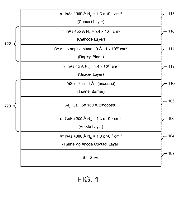
[0006] FIG. 1 is an example Antimonide-based non-uniform doping
heterostructure layer.
[0007] FIG. 2A is an example plot of current-voltage and curvature
characteristics for an
example detector that may utilize the example heterostructure layer of FIG. 1.
[0008] FIG. 2B is an example plot of current density versus voltage for three
example
heterostructure designs.
[0009] FIG. 3 illustrates energy band diagrams for two example detector
heterostructure
designs.
[0010] FIG. 4A illustrates junction capacitance versus voltage plots for
example cathode
designs.
[0011] FIG. 4B illustrates junction capacitance versus area and junction
resistance versus
area plots for a 7 A heterostructure.
[0012] FIG. 5 illustrates a plot of on-wafer sensitivity versus frequency for
the example
detector.
DETAILED DESCRIPTION
[0013] Technologies for millimeter-wave detection have been explored in recent
years for
applications in navigation, avionics, security screening, and chemical
sensing. Detection,
imaging, and/or radiometry of millimeter-waves may be accomplished using
devices made
with Silicon (Si), Germanium (Ge), GaAs, or other semiconductor materials in
an effort to
provide low noise, high pixel density, high nonlinearity and/or curvature,
and/or relatively
fast frequency responses. For example, Schottky diodes have been employed for
such
detection purposes due to their low forward turn-on voltage, fast frequency
response and high
-2-
CA 02725576 2010-11-24
WO 2010/016966 PCT/US2009/045288
bandwidth. While some Schottky diode implementations include external biasing,
which
introduces flicker noise (e.g., 1/f noise), unbiased implementations of
Schottky diodes still
generally suffer from strong sensitivity changes with temperature and may have
undesirably
large junction resistances. Further, Schottky diode temperature dependence
directly
influences diode curvature.
_ 321/3V2
Y l / aV Equation 1
a
< q Equation 2
kT
[0014] Example Equation 1 illustrates the curvature coefficient, y, which is
the quotient of
the second derivative of current-to-voltage divided by the first derivative of
current-to-
voltage. The curvature coefficient (y) serves as at least one industry-used
metric to quantify
detector nonlinearity (and hence sensitivity) at zero bias. However, as
described above,
Schottky diodes and/or other thermionic devices exhibit a fundamental
performance limit as
expressed in Equation 2, in which q is the electron charge, k is the Boltzmann
constant, and T
is the absolute temperature. Example Equation 2 is independent of device
design, and results
in a fundamental limit on Schottky diode curvature. Generally speaking, a
device exhibiting
relatively highly nonlinear current-voltage characteristics at zero bias
translates to improved
voltage sensitivity values for that device.
[0015] Ge-based backward tunnel diodes have also been studied in view of their
zero bias
nonlinearity. While zero bias devices simplify detector driver circuitry and
minimize
instances of added noise (e.g., flicker noise), Ge-based backward diodes
exhibit significant
manufacturing challenges that prevent cost judicious mass-producible devices
having
functional tolerances. Similar manufacturing challenges exist for GaAs-based
planar-doped
barrier diodes.
[0016] Example methods and apparatus described herein include InAs/AlSb/GaSb
backward diodes employed for millimeter-wave square-law power detection. Also
described
herein is, in part, a heterostructure design with a low junction capacitance,
a low junction
resistance, and a high curvature coefficient as compared to previously known
designs. The
example heterostructure design described herein includes a voltage
sensitivity, which is
directly proportional to the curvature coefficient that is improved by, for
example,
approximately 31% as compared to prior reports of devices having similar
barrier
thicknesses. These devices rely on, in part, quantum mechanical tunneling as a
basis of
-3-
CA 02725576 2010-11-24
WO 2010/016966 PCT/US2009/045288
operation. As such, such devices are not subject to one or more curvature
limitations, such as
those expressed above in Equation 2. The junction capacitance is also reduced
by, for
example, approximately 25% (e.g., 9.5 fF/ m2).
[0017] Improved sensitivity and decreased junction capacitance are realized,
in part, by
incorporation of a p-type 8-doping plane with an example sheet concentration
of 1 X 10¹² CM -2
in an example n-InAs cathode layer. The combination of low resistance (and
thus Johnson
noise) and high sensitivity result in an estimated noise equivalent power
(NEP) of 0.24
pW/Hz1/2 at 94 GHz for an example conjugately-matched source, while the
reduced
capacitance facilitates wideband matching and increases the example detector
cutoff
frequency. These antimonide (Sb)-based detectors have promise with, for
instance,
improving the performance of passive millimeter-wave and submillimeter-wave
imaging
systems.
[0018] Direct detection of millimeter-waves with zero bias square-law
detectors may be
particularly attractive for passive imaging applications because of the
reduced 1/f noise that
results from the absence of an external bias. Compared to alternatives
including, but not
limited to Schottky diodes, Ge backward diodes and GaAs planar-doped barrier
(PDB)
diodes, example InAs/AlSb/GaSb detectors demonstrate superior performance,
with high
sensitivity, high cut-off frequency, low noise, and favorable temperature-
dependence. While
low barrier zero bias Schottky diode detectors with tunable barrier heights
have been reported
at high frequencies, such diodes exhibit strong sensitivity changes with
temperature
compared to Sb-based tunnel diodes, particularly because the curvature (y) of
Schottky
diodes is typically limited to y<q/kT, as described above. At room temperature
(T=300 K), y
< 38.5 V-' for PDBs or Schottky diodes. On the other hand, the curvature of
the example
tunneling detectors described herein is not bounded by q/kT, and prior
demonstrations have
shown curvatures as high as 70 V-' for Ge-based devices. High curvature (y),
low
capacitance, C1, and modest junction resistance, Rj, are some example design
factors to
produce low noise detectors.
[0019] Reduction in Rj for Sb-heterostructure detectors has been achieved, in
part, by
reducing the tunnel barrier thickness from 32 A to approximately 7 A. However,
reducing
the barrier thickness alone also resulted in a corresponding decrease in
curvature coefficient
from 39 to 32 V-'. Described in further detail below are performance
characteristics of thin-
barrier Sb-based millimeter-wave detectors, in which some example
heterostructure designs
exhibit a measured curvature, y, of 42.4 V-'. Additionally, an example
measured unmatched
sensitivity, (3v, of 4200 V/W is realized by the methods and apparatus
described herein,
-4-
CA 02725576 2010-11-24
WO 2010/016966 PCT/US2009/045288
which is consistent with expectations from R, =2Zsy. This example curvature
exceeds the
theoretical limits for Schottky detectors, and may be achieved while
simultaneously reducing
the junction capacitance, C1. Improvements in sensitivity and capacitance may
be obtained
by tailoring the doping profile to include a p-type non-uniform (e.g., delta
(8)-doping plane,
ramp doping, pulse doping, etc.) in the heterostructure to optimize the charge
carrier
distribution within the example device(s). The example device design(s)
increase the zero
bias sensitivity and further lower the junction capacitance without
significantly
compromising the junction resistance. Such example characteristics are
particularly
applicable with, for instance, improving performance of low-noise millimeter-
wave and sub-
millimeter-wave detectors.
[0020] FIG. 1 illustrates an example device structure 100 grown by molecular
beam
epitaxy (MBE) on a semi-insulating GaAs substrate 102. Example metamorphic
device
layers are grown on a GaAs buffer, with a 4000 A n+ InAs (1.3x1019 cm 3)
tunneling anode
contact layer 104, a 300 A p+ GaSb (1.3x10¹⁹ CM-3 ) anode layer 106, a 150 A
undoped
Al0.1Ga0.9Sb layer 108, a 7-11 A undoped AlSb tunnel barrier 110, a 45 A n-
InAs spacer layer
(doped 1.4 x 1017 cm3) 112, a Be 8-doping plane (1 X 1012 cm-2) 114, a 455 A n-
InAs
(1.4x1017 cm3) cathode layer 116, and ending with an n+ InAs (1.3x1019 cm3)
contact layer
118. The addition of the example fully-depleted p-type 8-doping plane 114 in
the n-InAs
cathode layer 116 near the example AlSb barrier 110 adjusts the band bending
near the tunnel
barrier 110 to enhance the device performance. The example 45-A spacer layer
112 separates
the doping plane 114 from the tunnel barrier 110. Fabrication of example Sb-
based backward
diodes may be performed using, but not limited to mix-and-match electron-
beam/optical
lithography, contact metallization by evaporation and/or lift off, wet-
chemical mesa etching,
and/or benzocyclobutene dielectric passivation, and/or any other suitable
fabrication method.
[0021] In the illustrated example of FIG. 1, the thicknesses for the device
structure 100 are
provided for example purposes and not limitation. In some examples, greater or
lesser
thicknesses may be employed for the GaAs substrate 102, the tunneling anode
contact layer
104, the anode layer 106, the undoped AlGaSb layer 108, the tunnel barrier
110, the spacer
layer 112, the cathode layer 116, and/or the contact layer 118. Furthermore,
it should be
appreciated that the layer thicknesses may have a range of values in keeping
with the
described examples. Additionally, doping concentrations for the aforementioned
layers of
the example device structure 100 are provided for example purposes only and
not by way of
limitation.
-5-
CA 02725576 2010-11-24
WO 2010/016966 PCT/US2009/045288
[0022] Generally speaking, the example tunnel barrier 110, the undoped AlGaSb
layer 108,
and the anode layer 106 are referred to as an Antimonide (Sb) substructure
120.
Additionally, the example cathode layer 116, doping plane 114, and the spacer
layer 112 are
referred to as a cathode substructure 122. While the example doping plane 114
of FIG. 1
includes a Beryllium delta-doping plane, one or more alternate dopants may be
employed.
Moreover, one or more alternate non-uniform doping profiles may be employed
including,
but not limited to ramped doping profiles and/or pulsed doping profiles.
[0023] FIG. 2A shows the measured current-voltage and curvature
characteristics 200 for
an example 0.85X0.85 m2 area device, such as the example device 100 shown in
FIG. 1. In
the illustrated example of FIG. 2A, at zero bias 205, a junction resistance,
Rj, of 3239 S2 and a
high curvature of 42.4 V_1 are measured. Current density-voltage
characteristics of a detector
with the 8-doping plane and that of a device on an identical heterostructure
except with
uniform cathode doping are compared in an inset 210 of FIG. 2A. The example
inset 210 of
FIG. 2A is expanded in FIG. 2B, which illustrates a current-voltage comparison
between an
Sb heterostructure having a 10 A tunnel barrier 220 (see dash-dot line), an Sb
heterostructure
having a 7 A tunnel barrier 222 (see dashed line), and an Sb heterostructure
having a 7 A
tunnel barrier with 8-doping 224 (see solid line). As can be seen with 8-
doping 224 (solid
line), the example forward current (electrons tunneling from n-InAs (e.g., the
spacer layer
112 of FIG. 1) to the undoped Al0.1Ga0.9Sb layer (e.g., the undoped layer 108
of FIG. 1)) for
the 8-doped heterostructure (e.g., a detector) is strongly suppressed, while
the backward
current remains almost unchanged, resulting in an improved zero bias
curvature. In
operation, the example non-uniformly doped (e.g., 8-doped) plane 114 and Sb
tunnel barrier
110 improve device curvature by increasing the ratio of current on either side
of the zero bias
point 205.
[0024] FIG. 3 shows computed energy band diagrams 300 for a uniformly-doped
detector
304, 316 (dashed-lines) and a non-uniformly doped detector 302, 306 (solid
lines)
heterostructures. In the illustrated example of FIG. 3, a top-most solid line
302 represents the
conduction band of the non-uniformly doped (i.e., 8-doped) heterostructure,
and a top-most
dashed line 304 represents the conduction band of the uniformly doped
heterostructure. Also
shown in the illustrated example of FIG. 3, a lower-most solid line 306
represents the valence
band of the non-uniformly doped heterostructure, and a bottom-most dashed line
308
represents the valence band of the uniformly doped heterostructure. As can be
seen in the
example of FIG. 3, the addition of a fully-depleted p-type 8-doping plane 114
reduces the
band bending in the InAs cathode at an edge of the tunnel barrier 110, and
brings the
-6-
CA 02725576 2010-11-24
WO 2010/016966 PCT/US2009/045288
conduction band of the InAs close to the Fermi level Ef 310. For tunnel
diodes, this change
in band alignment more strongly suppresses the forward current flow than the
backward
current, thereby promoting an improved curvature coefficient.
fl = 2Zs y Equation 3.
[0025] As shown in the example Equation 3, device 100 sensitivity also
improves because
sensitivity (fy) is approximately directly proportional to the improved
curvature coefficient
(y), within typical approximations of an operational frequency well below the
cutoff
frequency of the detector.
[0026] In addition to the improvement in sensitivity (/3v), a lower junction
capacitance, C1,
may also be realized through the inclusion of the non-uniform doping plane
114, such as a 8-
doping plane, in the example cathode substructure 122. A junction capacitance
versus bias
chart 400 is shown in FIG. 4A, which was extracted from example bias-dependent
on-wafer
s-parameter measurements. In the illustrated example of FIG. 4A, the junction
capacitance
(C=) of a uniformly doped device 412 and/or a non-uniformly doped device 414
(e.g., a 8-
doped device) depends approximately linearly on (a) the applied bias for a
given
heterostructure, and (b) the specific capacitance for the given
heterostructure. FIG. 4A
illustrates, in part, that the example 8-doped detector 414 at zero bias is,
in one example, 13
fF/ m2, which is approximately 25% lower than that of devices without 8-doping
in the
cathode. The p-type 8-doping facilitates, in part, a lower capacitance by
reducing the
accumulation of electrons adjacent to the AlSb barrier 110 in the InAs cathode
116. Such
effects of the p-type 8-doping are also evident via the example band diagrams
300 of FIG. 3,
in which vertical lines denote computed centroids of incremental charges for a
small changes
in applied bias. FIG. 4B illustrates junction resistance (Ri, see trace 416)
and junction
capacitance (Ci, see trace 418) data extracted from on-wafer s-parameter
measurements as a
function of device area 420.
[0027] Returning briefly to FIG. 3, a left-most solid vertical line 312
represents the
centroid of incremental electron distribution for the example 8-doped
structure, and a right-
most solid vertical line 314 represents the centroid of incremental hole
distribution for the
example 8-doped structure. On the other hand, a left-most dashed vertical line
316 represents
the centroid of incremental electron distribution for an example uniformly
doped structure,
and a right-most dashed vertical line 318 represents the centroid of
incremental hole
distribution for the example uniformly doped structure. As shown by comparing
the example
8-doped structure centroids (312 and 314) with the example uniformly doped
structure
-7-
CA 02725576 2010-11-24
WO 2010/016966 PCT/US2009/045288
centroids (316 and 318), the example 8-doped structure exhibits a larger
spacing between
hole and electron charge centroids (WAQ). As a result, a lower capacitance is
realized when
employing the 8-doped structure as compared to the uniformly-doped structure.
Self-
consistent Poisson/Schrodinger calculations suggest that the 8-doping plane
may increase the
electron-hole separation from, in one example, 153 A to 239 A, for a reduction
in capacitance
of approximately 39%, which is in reasonable agreement with the measured
capacitance
change. Reduced capacitance may improve the intrinsic cutoff frequency, ff =
1/(2iRsCj),
and also reduce a reactive component of the example detector impedance and
ease the
realization of broadband matching. In this expression, Rs is the series
resistance of the
device, which is primarily limited by contact resistance. For 8-doped devices,
an example Rs
of 26 S2 may be realized, which results in an fc=620 GHz, which represents an
example rather
than a limitation. In other words, further improvements in such contact
resistances are
possible. A comparison of key figures of merit for uniformly-doped and 8-doped
structures
with 10 A thick tunnel barriers as an example is shown below in Table 1.
Device Type 7 (3v Ci Rj NEP
(V-') (V/W) (IF/ m2) (n m2) (pW/Hz"2)
8-Doped 42.4 4200 13 2340 0.24
Cathode
Uniform 32 3220 17.2 1340 0.29
Cathode
Table 1
[0028] As shown in Table 1, the junction resistance of the example 8-doped
structure is
increased from 1230 c m2 to 2340 S2 m2. While this increase in Rj leads to
increased
thermal noise, the overall detector NEP is improved because the increase in Rv
more than
offsets the increased thermal noise.
[0029] The millimeter-wave performance of 8-doped detectors is also assessed,
as
described in further detail below. FIG. 5 shows a measured on-wafer voltage
sensitivity
graph 500 for the example detector driven by a 50 S2 RF source from 1 to 110
GHz. The
example source was coupled to the device through a coaxial bias tee and on-
wafer probes,
and the detector voltage was measured at a DC arm of the bias tee. In the
illustrated example
of FIG. 5, the low frequency voltage sensitivity, P, is 4200 V/W, which is an
improvement
of approximately 31% from the previously-reported 3200 V/W for an identical
device except
with uniformly-doped cathode. An example nonlinear device model was extracted
using
bias-dependent s-parameter measurements and the example circuit model shown in
the inset
(410) of FIG. 4. In this example model, the series inductance, pad
capacitance, and series
-8-
CA 02725576 2010-11-24
WO 2010/016966 PCT/US2009/045288
resistance are bias independent, while the junction resistance and capacitance
vary with bias.
The parameters were found using nonlinear least-squares optimization of the
circuit model to
the measured s-parameters, with an additional constraint that the junction and
series
resistances were related to the measured DC I-V characteristics through
example Equation 4,
shown below.
al _ 1
aV (RS + R1) Equation 4.
[0030] Based on, in part, the aforementioned least-squares optimization of the
circuit
model, a Cp of 12 fF, Lp of 65 pH, and Rs of 26 S2 were extracted, and the
junction
capacitance (C1) is shown in FIG. 4. The frequency-dependence of the
sensitivity predicted
using the extracted nonlinear model agrees well with the measured sensitivity,
as shown in
FIG. 5. Extrapolation of the example circuit model projects an unmatched
sensitivity of 2000
V/W at 400 GHz. This experimental study of the frequency response shows the
potential of
Sb-heterostructure diodes as detectors at W band through Y-band and beyond.
[0031] The optimum sensitivity, (3opt, that may result from the inclusion of a
lossless
matching network between the source and detector was projected from the
measured
unmatched sensitivity with an example 50-a source in conjunction with the
measured s-
parameters. The low-frequency (3opt with an example conjugately matched source
is
calculated to be, in this example, 8.0X10⁴ V/W, and is 3.0X10⁴ V/W at 94 GHz.
In view of
these example devices experimentally showing thermal-noise limitations for
small incident
powers, the corresponding noise equivalent power for the detector operated at
94 GHz is
estimated to be 0.24 pW/Hz"2 based on the measured junction resistance. This
is an
improvement of approximately 17% over the NEP of a typical uniformly doped
cathode
device. The combination of high sensitivity and low noise makes the example Sb-
heterostructure detectors described herein promising for passive millimeter-
wave imaging
sensors without RF pre-amplification.
[0032] Table 2 illustrates additional example figures of merit for the three
example
heterostructures shown in FIG. 2B, in which noise equivalent temperature
difference (NETD)
values are calculated for matched sensitivity with an ideal band-pass lossless
matching
network at 94 GHz. These are example data from fabricated devices and do not
imply
fundamental limitations, but do illustrate example observed trends.
Structure 10 A 7 A 7 A with 8-doping
Relative y (%) 100 88 100
R1 (S2. m) 1045 353 369
-9-
CA 02725576 2010-11-24
WO 2010/016966 PCT/US2009/045288
C1 (fF/ m) 8.5 10.5 9.5
Rs (S2. m) 22 28 23
fT (GHz) 852 541 729
NETD (K) 7.14 3.51 3.24
RL = 16dB
Af (GHz) 30 71 75
Table 2
[0033] As illustrated by Table 2, implementation of the non-uniform doping,
such as 8-
doping, with an Sb tunnel barrier breaks previous tightly linked trade-offs
between junction
resistance (Rj) and curvature (y). In Table 2, for ease of comparison, the
curvature (y) has
been normalized to the value obtained for the 10 A barrier devices. By
introducing the 8-
doping, curvatures are improved while maintaining lower values of Rj.
[0034] Example InAs/AlSb/GaSb backward diode detectors with an improved
heterostructure design have shown a high curvature of 42.4 V-' and reduced
capacitance.
This corresponds to an unmatched sensitivity of 4200 V/W, exceeding the
theoretical limits
of Schottky diodes. The improved sensitivity and decreased junction
capacitance for the
example detectors described herein originate from the example modified device
heterostructure, which incorporates a fully-depleted p-type 8-doping plane
with sheet
concentration of 1 X 10¹² CM -2 in the n-InAs cathode layer. The high
sensitivity and low
junction resistance result in an estimated NEP of 0.24 pW/Hz1/2 at 94 GHz for
a conjugately-
matched source, making it a promising candidate for passive imaging sensors at
room
temperature without RF pre-amplification. Moreover, example detectors with
this
heterostructure have reduced junction capacitance that offers the potential
for operation
through Y band and beyond.
[0035] Although certain example methods and apparatus have been described
herein, the
scope of coverage of this patent is not limited thereto. On the contrary, this
patent covers all
methods and apparatus fairly falling within the scope of the appended claims
either literally
or under the doctrine of equivalents.
-10-