Note: Descriptions are shown in the official language in which they were submitted.
CA 02725632 2010-11-24
WO 2009/144715 PCT/IL2009/000520
A MONOLITHIC LOW CONCENTRATION PHOTOVOLTAIC PANEL
BASED ON POLYMER EMBEDDED PHOTOVOLTAIC CELLS AND
CROSSED COMPOUND PARABOLIC CONCENTRATORS
FIELD OF THE DISCLOSED TECHNIQUE
The disclosed technique relates to concentrating photovoltaic
panels in general, and to a monolithic concentrating photovoltaic solar
panel based on polymer embedded photovoltaic cells, interconnects, and
crossed Compound Parabolic Concentrators (CPC), in particular.
BACKGROUND OF THE DISCLOSED TECHNIQUE
In flat panel photovoltaic technologies (e.g., based on
mono-crystalline silicon wafers, poly-crystalline silicon wafers,
multi-junction cells and tandem cells), the cost of the photovoltaic material
dictates a large portion of the total panel cost. For example, in case of
mono-crystalline based solar panels, the cost of silicon wafers carries
approximately 65% of the total panel cost.
Concentrating photovoltaic technologies are employed in order
to reduce the photovoltaic material content of the solar panel, thereby,
reducing its cost. Expensive photovoltaic materials are replaced by
relatively cheap lenses and optical concentrators. The larger the optical
concentration value of the system (i.e., the amount of light radiation energy
focused onto a specific surface area), the lower will be the total active
photovoltaic area of the system.
Reference is now made to Figure 1, which is a schematic
illustration of a concentrating photovoltaic device, generally referenced 10,
constructed and operative as known in the art. Concentrating photovoltaic
3o device 10 includes a photovoltaic cell 12, a substrate 14, a plurality of
-1-
CA 02725632 2010-11-24
WO 2009/144715 PCT/IL2009/000520
interconnects 16, a plurality of wires 18 and a lens 20. Photovoltaic cell 12
is positioned on top of substrate, 14, approximately in the center thereof.
Photovoltaic cell 12 can be any photovoltaic cell known in the art, such as
a mono-crystalline silicon cell, a poly-crystalline silicon cell, a multi-
junction
cell, or a tandem cell. Photovoltaic cell 12 converts light radiation into
electrical current. Substrate 14 functions as a structural base and as a
heat sink.
Wires 18 transfer the generated electrical current from
photovoltaic cell 12 to interconnects 16. Lens 20 is a concentrating lens,
Io which concentrates light radiation toward photovoltaic cell 12. For
example, lens 20 concentrates each of parallel beams 22A, 24A and 26A
toward photovoltaic cell 12. Each of concentrated beams 22B, 24B and
26B corresponds to each of un-concentrated parallel beams 22A, 24A and
26A. The distance of between lens 20 and photovoltaic cell 12 is
determined by the value of a depth of focus of concentrating photovoltaic
device 10. The value of the depth of focus of concentrating photovoltaic
device 10 is related to the concentration power and the design of lens 20,
and of the size of photovoltaic cell 12.
In most concentrating photovoltaic panels that include an array
of concentrating photovoltaic devices (e.g., photovoltaic device 10), each
photovoltaic cell is assembled and interconnected individually. At high
optical concentration values, the total active photovoltaic area required by
the system is small, and hence small sized photovoltaic cells are
employed. For example, in high optical concentration applications,
photovoltaic cells with areas down to 4 millimeters square are employed.
A view angle is the angle of incoming light beams, which an
optical element can receive (i.e., field of view). Low concentration
photovoltaic devices operate at high view angles (i.e., large field of view),
and thus do not require mechanical sun tracking devices. Optical
concentrations of up to a factor of ten are employed in low concentration
photovoltaic devices. In prior art systems, at low optical concentration
-2-
CA 02725632 2010-11-24
WO 2009/144715 PCT/IL2009/000520
values, the total active photovoltaic area required by the system is large,
and hence small sized photovoltaic cells are rarely employed.
-3-
CA 02725632 2010-11-24
WO 2009/144715 PCT/IL2009/000520
SUMMARY OF THE PRESENT DISCLOSED TECHNIQUE
It is an object of the disclosed technique to provide a monolithic
concentrating photovoltaic solar panel based on polymer embedded
photovoltaic cells, interconnects, and crossed Compound Parabolic
Concentrators and a method for the production thereof.
In accordance with an embodiment of the disclosed technique,
there is thus provided a concentrating photovoltaic panel. The panel
includes an encapsulating polymer layer, an array of photovoltaic cells, a
plurality of first interconnects and an optical layer. Each of the
io photovoltaic cells is embedded within the encapsulating layer. The
plurality of first interconnects is coupled with each of the photovoltaic
cells
and with the encapsulating layer. The plurality of first interconnects
electrically interconnect all the photovoltaic cells of the array there
between. The optical layer is coupled on top of the encapsulating layer
1s and the array of photovoltaic cells. The optical layer concentrates light
radiation onto the array of photovoltaic cells. At least one of the plurality
of
first interconnects remains exposed out of the protective layer.
In accordance with another embodiment of the disclosed
technique, there is thus provided a method for producing a photovoltaic
20 concentrating panel. The method includes the following procedures,
forming a matrix layer, forming a first interconnecting layer, forming a
protective layer and forming an optical layer. The procedure of forming a
matrix layer is performed by embedding an array of photovoltaic cells
within a polymer resin material. The procedure of forming a first
25 interconnecting layer is performed by electrically coupling between
terminals of the photovoltaic cells. The procedure of forming a protective
layer includes forming at least one opening in the protective layer. The
procedure of forming an optical layer is performed such that each of a
plurality of parabolic concentrators is optically coupled with a respective
30 one of the array of photovoltaic cells.
-4-
CA 02725632 2010-11-24
WO 2009/144715 PCT/IL2009/000520
In accordance with a further embodiment of the disclosed
technique, there is thus provided a photovoltaic cell. The photovoltaic cell
includes an N type doped semiconductor layer, a P type doped
semiconductor layer, a passivation layer and a high concentration doped
layer. The P type layer is positioned on the top surface of the N type layer.
The size of the surface area of the bottom surface of the N type layer is
larger than that of the top surface of the P type layer. The passivation
layer is positioned on the top surface of the P type layer. The passivation
layer provides passivation protection to the photovoltaic cell. The high
concentration doped layer covers all sides of the P type layer and of the N
type layer. The doping concentration of the high concentration doped
layer is larger than that of each of the P type layer and the N type layer by
at least two orders of magnitude. The high concentration doped layer is
tilted with respect to the normal to the top surface of the P type layer.
-5-
CA 02725632 2010-11-24
WO 2009/144715 PCT/IL2009/000520
BRIEF DESCRIPTION OF THE DRAWINGS
The disclosed technique will be understood and appreciated
more fully from the following detailed description taken in conjunction with
the drawings in which:
Figure 1 is a schematic illustration of a concentrating
photovoltaic device, constructed and operative as known in the art;
Figure 2A is a schematic illustration of a top view of a chip-sized
photovoltaic cell, constructed and operative in accordance with an
embodiment of the disclosed technique;
Figure 2B is a schematic illustration of a bottom view of the
chip-sized photovoltaic cell of Figure 2A;
Figure 2C is a schematic illustration of a cross section view of
the chip-sized photovoltaic cell of Figure 2A;
Figure 3A is a schematic illustration of a cross section of a
concentrating photovoltaic panel, constructed and operative in accordance
with another embodiment of, the disclosed technique;
Figure 3B is a schematic illustration of the optical layer of Figure
3A;
Figures 4A and 4B are schematic illustrations of a concentrating
photovoltaic panel, constructed and operative in accordance with a further
embodiment of the disclosed technique;
Figure 5 is a schematic illustration of a cross section of a
concentrating photovoltaic panel, constructed and operative in accordance
with another embodiment of the disclosed technique;
Figure 6A is a schematic illustration of a bottom view of a
concentrating photovoltaic panel, constructed and operative in accordance
with a further embodiment of the disclosed technique;
Figure 6B is a schematic illustration of a top view of the
photovoltaic panel of Figure 6A;
-6-
CA 02725632 2010-11-24
WO 2009/144715 PCT/IL2009/000520
Figure 7A is a schematic illustration of a top view of a chip-sized
photovoltaic cell, constructed and operative in accordance with another
embodiment of the disclosed technique;
Figure 7B is a cross section view of the photovoltaic cell of
Figure 7A;
Figure 7C is a bottom view of the photovoltaic cell of figure 7A;
Figure 8 is a schematic illustration of a cross section of a
concentrating photovoltaic panel, constructed and operative in accordance
with a further embodiment of the disclosed technique;
Figure 9 is a schematic illustration of a bottom view of an
interconnect of a photovoltaic cell, constructed and operative in
accordance with another embodiment of the disclosed technique;
Figure 10 is a schematic illustration of a bottom view of an
interconnects platform of a photovoltaic panel, constructed and operative
in accordance with a further embodiment of the disclosed technique;
Figure 10B is an enlarged view of a segment of Figure 10A;
Figure 11 is a schematic illustration of a bottom view of an
interconnects platform of a photovoltaic panel, constructed and operative
in accordance with another embodiment of the disclosed technique; and
Figure 12 is a schematic illustration of a block diagram of a
method for constructing a concentrating photovoltaic panel, operative in
accordance with a further embodiment of the disclosed technique.
-7-
CA 02725632 2010-11-24
WO 2009/144715 PCT/IL2009/000520
DETAILED DESCRIPTION OF THE EMBODIMENTS
The disclosed technique overcomes the disadvantages of the
prior art by providing a monolithic concentrated solar panel including a
plurality of polymer embedded photovoltaic cells, a plurality of
interconnects and a plurality of crossed compound parabolic
concentrators.
Reference is now made to Figures 2A, 2B and 2C. Figure 2A is
a schematic illustration of a top view of a chip-sized photovoltaic cell,
generally referenced 100, constructed and operative in accordance with an
embodiment of the disclosed technique. Figure 2B is a schematic
illustration of a bottom view of the chip-sized photovoltaic cell of Figure
2A.
Figure 2C is a schematic illustration of a cross section view of the
chip-sized photovoltaic cell of Figure 2A. Photovoltaic cell 100 includes a
P-type doped semiconductor (e.g., silicon) layer 102, an N-type doped
semiconductor layer 106, a passivation layer 104 and a high concentration
doped layer 108 (i.e., a layer having a high doping concentration, as
detailed herein below).
P-type layer 102 is coupled on top of N-type layer 106, such that
it covers a top surface 112 of N-type layer 106. Passivation layer 104 is
coupled on a top surface 114 of P-type layer 102. The size of top surface
114 of P-type layer 102 is larger than that of the bottom surface (not
shown) of passivation layer 104, such that passivation layer 104 does not
fully cover top surface 114 of P-type layer 102. High concentration doped
layer 108 covers the side wall surfaces of both P-type layer 102 and
N-type layer 106. The size of the surface area of a bottom surface 110 of
N-type layer 106 is larger than that of top surface 114 of P-type layer 102.
Chip-sized photovoltaic cell 100 is made of mono-crystalline
semiconductor (e.g., silicon - produced by a Float Zone or a Czochralski
process), or poly-crystalline semiconductor. The shape of the top surface
of photovoltaic cell 100 is rectangular (e.g., a square or a rectangle). It is
noted that, the positions of P-type layer 102 and N-type layer 106 can be
-8-
CA 02725632 2010-11-24
WO 2009/144715 PCT/IL2009/000520
interchanged. The top surface of P-type layer 102 is either smooth or
textured.
Passivation layer 104 is made of silicon nitride, or silicon oxide.
Passivation layer 104 provides passivation and anti-reflection protection to
photovoltaic cell 100. Passivation layer 104 bonds to dangling silicon
bonds (not shown) located at the surface of the silicon crystal lattice of
P-type layer 102. Passivation layer 104 passivates the dangling silicon
bonds, thereby lowering energy losses due to charge recombination. The
refraction index of passivation layer 104 is lower than the refraction index
of P-type layer 102. In this manner, the amount of light radiation, which is
reflected back out of photovoltaic cell 100 through passivation layer 104, is
reduced. Therefore, the efficiency of photovoltaic cell increases.
The edges (not shown) of top surface 114 of P-type layer 102
are exposed for coupling interconnects (not shown for example, top
interconnects 158 of Figure 3A). Bottom surface 110 of N-type layer 106
is exposed. Alternatively, bottom surface 110 is covered with an aluminum
layer (Al-BSF) for improving the metal contact thereof.
High concentration doped layer 108 is made of silicon oxide (i.e.,
substantially similar to passivation layer 104). Alternatively, high
concentration doped layer 108 is made of doped semiconductor. The
doping concentration of high concentration doped layer 108 is higher than
the doping concentration of each of P-type layer 102 and N-type layer 106
by substantially two orders of magnitude, or more. High doping
passivation layer 108 is implanted with minority carrier atoms for producing
an electric field which would repel the minority carriers within the adjacent
Silicon doped layer from reaching the edge. For example, in the portion of
high doping layer 108 adjacent P-type layer 102, layer 108 is doped
implanted with N-type ions, thus the N-type ions produce a magnetic field
which repels negative charge carriers within P-type layer 102.
As detailed herein above, the surface area of the bottom surface
of N-type layer 106 is larger than that of top surface 114 of P-type layer
-9-
CA 02725632 2010-11-24
WO 2009/144715 PCT/IL2009/000520
102. High concentration doped layer 108 is tilted at an angle of a with
respect to a normal 116 to top surface 114. The tilt angle a enables
implanting of high concentration doped layer 108 by employing an implant
doping procedure (i.e., bombarding high concentration doped layer 108
with a strong vertical ion beam).
It is noted that, the size of chip-sized photovoltaic cell 100
ranges between 0.25 to 400 millimeters square. Light radiation impinges
on photovoltaic cell 100. The light radiation enters into photovoltaic cell
100 through passivation layer 104. Photovoltaic cell 100 absorbs the light
1o radiation and generates an electric, current (i.e., a P-N junction solar
cell).
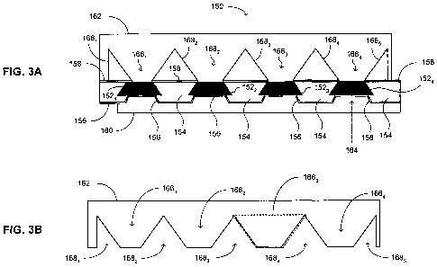
Reference is now made to Figures 3A and 3B. Figure 3A is a
schematic illustration of a cross section of a concentrating photovoltaic
panel, generally referenced 150, constructed and operative in accordance
with another embodiment of the disclosed technique. Figure 3B is a
schematic illustration of the optical layer of Figure 3A. Photovoltaic panel
150 includes an array of four photovoltaic cells 1521, 1522, 1523 and 1524,
an encapsulating polymer layer 154, a bottom interconnects layer 156, a
top interconnects layer 158, a bottom protective layer 160 and an optical
layer 162. Each of photovoltaic cells 1521, 1522, 1523 and 1524 is
embedded within encapsulating layer 154. Bottom interconnects layer 156
is coupled with the bottom surfaces (not shown) of both photovoltaic cells
1521, 1522, 1523 and 1524 and of encapsulating layer 154 (i.e., bottom.
interconnects layer 156 electrically interconnect the bottom surfaces of
photovoltaic cells 1521, 1522, 1523 and 1524). Top interconnects layer 158
is coupled between photovoltaic cells 1521, 1522, 1523 and 1524 at the top
surfaces thereof (i.e., top interconnects layer 158 electrically interconnect
the top surfaces of photovoltaic cells 1521, 1522, 1523 and 1524).
Encapsulating polymer layer 154 is coupled between protective layer, 160
(i.e., which covers the bottom of bottom interconnects layer 156) and
optical layer 162 (i.e., which covers the top of top interconnects layer 158).
-10-
CA 02725632 2010-11-24
WO 2009/144715 PCT/IL2009/000520
Each of Photovoltaic cells 1521, 1522, 1523 and 1524 is a
chip-sized photovoltaic cell, substantially similar to photovoltaic cell 100
of
Figures 2A, 2B and 2C. Encapsulating polymer layer 154 is made of a
polymer such as polyolefin-based block copolymers, and the like.
Encapsulating polymer layer 154 maintains photovoltaic cells 1521, 1522,
1523 and 1524 in position and supports bottom interconnects layer 156 and
top interconnects layer 158. Encapsulating layer 154 absorbs stresses
arising from mismatches of thermal expansion coefficients between
components of photovoltaic panel 150 (e.g., photovoltaic cells 1521, 1522,
1523 and 1524 and bottom interconnects layer 156). Encapsulating layer
154 encapsulates photovoltaic cells 1521, 1522, 1523 and 1524, which are
embedded therein. In other words, encapsulating layer 154 covers all
sides, and partially the bottom surface (not shown) of each of photovoltaic
cells 1521, 1522, 1523 and 1524-
Bottom interconnects layer 156 is made of an electrically
conductive metal, such as copper, aluminum, tungsten and the like.
Alternatively, bottom interconnects layer 156 is made of an electrically
conductive metal stack, such as nickel-copper and the like. As detailed
herein above, bottom interconnects layer 156 is coupled with the bottom
surface (not shown) of encapsulating layer 154, and with the exposed
areas of the bottom surface (not shown) of photovoltaic cells 1521, 1522,
1523 and 1524. Bottom interconnects layer 156 electrically interconnects
the bottom surfaces of all photovoltaic cells 152,, 1522, 1523 and 1524.
Bottom interconnects layer 156 thermally interconnects photovoltaic cells
1521, 1522, 1523 and 1524 and conduct excess heat out of photovoltaic
panel 150. In other words, bottom interconnects layer 156 further
functions as a heat sink for photovoltaic panel 150.
Top interconnects layer 158 is made of an electrically conductive
metal, such as copper, aluminum and the like. Alternatively, Top
interconnects layer 158 is made of an electrically conductive metal stack,
such as nickel-copper and the like. Top interconnects layer 158 is coupled
-11-
CA 02725632 2010-11-24
WO 2009/144715 PCT/IL2009/000520
with the top surface (not shown) of encapsulating layer 154, and with the
exposed P-type doped semiconductor edges on the top surface of
photovoltaic cells 1521, 1522, 1523 and 1524 (e.g., the edges of the top
surface of P-type layer 102 of Figure 2C). Top interconnects layer 158
electrically interconnects the top surfaces of all photovoltaic cells 1521,
1522,1523 and 1524.
Protective layer 160 is made of a protective polymer such as
Polyvinylidene Fluoride (PVDF), polymethyl methacrylate, polycarbonate
and the like. Protective layer 160 covers the bottom side of photovoltaic
panel 150 (i.e., bottom interconnects layer 156) and provides
environmental protection thereto. One end of bottom interconnects layer
156 remains exposed such that it provides an electrical connection to an
external electrical system (e.g., a power grid). In the example set forth in
Figure 3A, the left hand side end of bottom interconnects layer 156
1s remains exposed, and is not covered by protective layer 160.
Alternatively, a plurality of locations of bottom interconnects layer 156 are
exposed, thereby providing additional electrical connections.
Optical layer 162 covers top interconnects layer 158. One end
of top interconnects layer 158 is exposed, such that it provides an
electrical connection to external electrical system. Alternatively, a
plurality
of locations of top interconnects layer 158 are exposed, thereby providing
additional electrical connections. It is noted that, top interconnects layer
158 and bottom interconnects layer 156 electrically interconnect
photovoltaic cells 1521, 1522,1523 and 1524 in-parallel.
Optical layer 162 is made of optically transparent polymers
having a high index of refraction such as polymethyl methacrylate,
polycarbonate, and the like. Optical layer 162 includes an array of
inverted truncated triangles 1661, 1662, 1663 and 1664 (i.e., CPCs 1661,
1662, 1663 and 1664). In the example set forth in Figure 3B, CPC 1663 is
3o depicted as surrounded with a dotted frame for better understanding of its
shape. Each of CPCs 1661, 1662, 1663 and 1664 is positioned on top of
-12-
CA 02725632 2010-11-24
WO 2009/144715 PCT/IL2009/000520
each of photovoltaic cell 1521, 1522, 1523 and 1524, respectively. The
volume between CPCs 1661, 1662, 1663 and 1664 is of the shape of an
array of hollow triangles 1681, 1682, 1683, 1684 and 1685. The truncated
end (i.e., the exit aperture - not shown) of each of CPCs 1661, 1662, 1663
and 1664 is positioned adjacent to the top surface of each of photovoltaic
cells 1521, 1522, 1523 and 1524, respectively, and is optically coupled
therewith. The refraction index of each of CPCs 1661, 1662, 1663 and 1664
is higher than that of each of hollow triangles 1681, 1682, 1683, 1684 and
1685. In this manner, each CPC 1661, 1662, 1663 and 1664 concentrates
light onto each of photovoltaic cells 1521, 1522,1523 and 1524, respectively,
by total internal reflection. Alternatively, at least a portion of array of
hollow triangles 1681, 1682, 1683, 1684 and 1685 is replaced by triangles
filled with a material having refraction index lower than that of optical
layer
162. Alternatively, photovoltaic panel 150 includes any number of
photovoltaic cells, CPCs, and hollow triangles, such as hundred, thousand,
and ten thousand photovoltaic cells and respective CPCs.
A layer of vias 164 Is etched through encapsulating layer 154.
The position of each via of vias layer 164 corresponds to the position of a
respective one of photovoltaic cells 1521, 1522, 1523 and 1524. Each via
164 exposes (i.e., vias 164 provide openings through encapsulating layer
154, thereby exposing photovoltaic cells 1521, 1522, 1523 and 1524 out of
encapsulating layer 154) a portion of the bottom surface (not shown) of the
respective one of photovoltaic cells 1521, 1522, 1523 and 1524. Light
radiation enters photovoltaic panel 150 through the top surface (not
shown) of optical layer 162. The light is concentrated through total internal
reflection by each of CPCs 166,, 1662, 1663 and 1664. The concentrated
light exits optical layer 162 toward the silicon nitride passivation layer
(i.e.,
passivation layer 104 of Figure 2C) on the top surface of photovoltaic cells
1521, 1522, 1523 and 1524, respectively. Each of photovoltaic cells 1521,
1522, 1523 and 1524 converts the solar radiation into electrical current.
Bottom interconnects layer 156 and top interconnects layer 158 conduct
-13-
CA 02725632 2010-11-24
WO 2009/144715 PCT/IL2009/000520
the electrical current from photovoltaic cells 152,, 1522, 1523 and 1524 to
the electrical connections of photovoltaic panel 150. Bottom interconnects
layer 156 further conducts heat away photovoltaic panel 150.
Reference is now made to figures 4A and 4B which are
schematic illustrations of a concentrating photovoltaic panel, generally
referenced 200, constructed and operative in accordance with a further
embodiment of the disclosed technique. Figure 4A is a bottom view of
concentrating photovoltaic panel 200. Figure 4B is a schematic illustration
of a top view of the photovoltaic panel 200. Photovoltaic panel 200
includes a polymer encapsulating layer 202, an optical layer 204, a
peripheral top contact pad 206, a protective polymer layer 208, and a
peripheral bottom contact pad 210. Optical layer 204 covers the top
surface (not shown) of encapsulating polymer layer 202. Peripheral top
contact pad 206 is positioned on the periphery of the top surface of
1s polymer layer 202, adjacent to optical layer 204. In the example set forth
in Figure 4A, contact pad 206 is positioned on the right hand side of the
top surface of polymer layer 202.
Polymer encapsulating layer 202 is substantially similar to
encapsulating layer 154 of Figure 3A. Encapsulating layer 202
encapsulates a plurality of photovoltaic cells (not shown - e.g.,
photovoltaic cell 100 of Figures 2A, 2B and 2C), which are embedded
therein. Optical layer 204 is substantially similar to optical layer 162 of
Figure 3A.
Optical layer 204 includes a plurality of crossed Compound
Parabolic Concentrators (CPCs), substantially similar to CPCs 1661, 1662,
1663 and 1664 of Figure 3A. A plurality of interconnects (not shown) are
embedded between polymer encapsulating layer 202 and optical layer
204. Periphery contact pad 206 is made of an electrically conductive
material, such as copper, aluminum, and the like. Periphery contact pad
3o 206 provides an electrical connection for photovoltaic panel 200 (e.g.,
-14-
CA 02725632 2010-11-24
WO 2009/144715 PCT/IL2009/000520
periphery top contact pad 106 connects photovoltaic panel 200 to an
external system, such as an electrical power grid).
Photovoltaic panel 200 further includes a protective layer 208
and a periphery bottom contact pad 210. Protective layer 208 is
positioned on the bottom surface (not shown) of encapsulating polymer
layer 202. Periphery bottom contact pad 210 is positioned on the
periphery of the bottom surface of encapsulating polymer layer 202,
adjacent protective layer 208. In the example set forth in Figure 4A,
periphery bottom contact pad 210 is positioned on the left hand side of
protective layer 208.
Protective layer 208 is substantially similar to protective layer
160 of Figure 3A. Protective layer 208 covers the bottom side of
photovoltaic panel 200 and provides environmental protection thereto.
Periphery bottom contact pad 210 is made of electrically conductive
1s material, such as copper, aluminum and the like. Periphery bottom
contact pad 210 connects photovoltaic panel 200 to an external system
(e.g., an electrical power grid).
Reference is now made to Figure 5, which is a schematic
illustration of a cross section of a concentrating photovoltaic panel,
generally referenced 250, constructed and operative in accordance with
another embodiment of the disclosed technique. Concentrating
photovoltaic panel 250 includes a plurality of photovoltaic cells 252, an
encapsulating polymer layer 254, a layer of bottom interconnects 256, a
layer of top interconnects 258, a protective layer 260, an optical layer 262
and an array of conductive plugs 268.
Each of photovoltaic cells 252, encapsulating layer 254, bottom
interconnects layer 256, top interconnects layer 258, protective layer 260
and optical layer 262 (including CPCs 266 and triangles 268) is
substantially similar to photovoltaic cells 1521, 1522, 1523 and 1524,
3o encapsulating layer 154, bottom interconnects layer 156, top interconnects
layer 158, protective layer 160 and optical layer 162 (including CPCs 1521,
-15-
CA 02725632 2010-11-24
WO 2009/144715 PCT/IL2009/000520
1662, 1663 and 1664 and triangles 1681, 1682, 1683, 1684 and 1685) of
Figure 3A, respectively.
Each of conductive plugs 268 is made of an electrically
conductive material, such as copper, nickel, tungsten, and the like. The
shape of the surface of conductive plugs 268 is rectangular (e.g., square
or rectangle). Encapsulating layer 254 covers all sides of each of
conductive plugs 268 (i.e., conductive plugs 268 are embedded within
encapsulating layer 254).
Bottom interconnects layer 256 electrically interconnects the
bottom surface (not shown) of each of photovoltaic cells 252 to an
adjacent conductive plug 268. Top interconnects layer 258 electrically
interconnects the top surface of each of photovoltaic cells 252 to an
adjacent conductive plug 268. In the example set forth in Figure 5, bottom
interconnects layer 256 interconnects each photovoltaic cell 252 to an
adjacent conductive plug 268 positioned on the right hand side of that
photovoltaic cell 252. In the example set forth in Figure 5, top
interconnects layer 258 interconnects each photovoltaic cell 252 to an
adjacent conductive plug 268 positioned on the left hand side of that
photovoltaic cell 252. In this manner, Top interconnects layer 258 and
bottom interconnects layer 256 electrically interconnect photovoltaic cells
252 in-series. Each of a plurality of vias 264 is positioned below each of
photovoltaic cells 252, thereby exposing at least a portion of the bottom
surface of the respective photovoltaic cell 252 (i.e., exposing out of
encapsulating layer 254). Each of a plurality of vias 270 is positioned
below each of conductive plugs 268, thereby exposing at least a portion of
the bottom surface of the respective conductive plug 268. Alternatively, at
least a first portion of the photovoltaic cells (e.g., cells 1521, 1522, 1523
and
1524 and 252 of Figures 3A and 5, respectively) included in the
concentrated photovoltaic panel (e.g., panel 200 of Figures 4A and 4B)
are interconnected in-parallel, and at least another portion of the
photovoltaic cells are interconnected in-series.
-16-
CA 02725632 2010-11-24
WO 2009/144715 PCT/IL2009/000520
Reference is now made to Figures 6A and 6B. Figure 6A is a
schematic illustration of a bottom view of a concentrating photovoltaic
panel, generally referenced 300, constructed and operative in accordance
with a further embodiment of the disclosed technique. Figure 6B is a
schematic illustration of a top view of the photovoltaic panel of Figure 6A.
Photovoltaic panel 300 includes an encapsulating polymer layer 302, an
optical layer 304, a protective layer 306, a first bottom contact pad 308 and
a second bottom contact pad 310. Encapsulating layer 302 is coupled
between optical layer 304 and protective layer 306. First contact pad 308
is coupled on the bottom surface of encapsulating layer 302 adjacent
protective layer 306 (i.e., on a first hand side of protective layer). Second
contact pad 310 is coupled on the bottom surface of encapsulating layer
302 adjacent protective layer 306, opposite to first contact pad 308 (i.e., on
a second hand side of protective layer, opposite to the first hand side).
Each of encapsulating polymer layer 302, optical layer 304 and
protective layer 306 is substantially similar to encapsulating polymer layer
154, optical layer 162 and protective layer 160 of Figure 3A, respectively.
Encapsulating layer 302 includes a plurality of photovoltaic cells (not
shown) substantially similar to photovoltaic cell 350 of Figures 7A, 7B and
7C (i.e., rear contact cell). Optical layer 304 includes a plurality of
crossed
CPCs (not shown) substantially similar to CPCs 1661, 1662, 1663 and 1664
of Figure 3A. Each of first contact pad 308 and second contact pad 310 is
substantially similar to bottom contact pad 210 of Figure 4A.
Reference is now made to Figures 7A, 7B and 7C. Figure 7A is
a schematic illustration of a top view of a chip-sized photovoltaic cell,
generally referenced 350, constructed and operative in accordance with
another embodiment of the disclosed technique. Figure 7B is a cross
section view of the photovoltaic cell of Figure 7A. Figure 7C is a bottom
view of the photovoltaic cell of figure 7A. Photovoltaic cell 350 includes a
first passivation layer 352, a first N-type doped silicon layer 354 (i.e.,
N-type layer - emitter layer 354), a first P-type doped silicon layer 356
-17-
CA 02725632 2010-11-24
WO 2009/144715 PCT/IL2009/000520
(i.e., P-type layer - base layer 356), a second P-type layer 358, a second
N-type layer 360, a second passivation layer 362 and high concentration
doped layer 366.
First passivation layer 352 covers the top surface (not shown) of
emitter layer 354. Emitter layer 354 covers the top surface of base layer
356. The surface area of the top surface of emitter layer 354 is smaller
than the surface area of the bottom surface (not shown) of base layer 356.
Second P-type layer 358 and second N-type layer 360 are integrated such
that they form a checkered pattern layer (not shown). The checkered
io pattern layer of second- P-type layer 358 and second N-type layer 360 is
coupled with the bottom surface of base layer 356. Second passivation
layer 362 covers the bottom surface (not shown) of the checkered pattern
layer of second P-type layer 358 and second N-type layer 360. High
concentration doped layer 366 covers all side surfaces (not shown) of
photovoltaic cell 350.
Photovoltaic cell 350 is a rear contact solar cell (i.e., the
electrical connections thereof are positioned on the bottom thereof).
Photovoltaic cell 350 is made of mono-crystalline silicon (i.e., produced by
a Float Zone or a Czochralski process). The shape of the top surface (not
shown) of photovoltaic cell 350 (i.e., of first passivation layer 352) is
rectangular (e.g., a square or a rectangle).
Each of first passivation layer 352, emitter layer 354, base layer
356 and High concentration doped layer 366 is substantially similar to
passivation layer 104, P-type doped silicon layer 102, N-type doped silicon
layer 106 and high concentration doped layer 108 of Figures 2A, 2B and
2C, respectively.
Second passivation layer 362 is a passivation layer made of
silicon oxide or polyimide. Second passivation layer 362 prevents
electrical shorts (i.e., second passivation layer 362 is an electrical
insulation layer). Second passivation layer 362 covers the checkered
pattern layer of second P-type layer 358 and second N-type layer 360.
-18-
CA 02725632 2010-11-24
WO 2009/144715 PCT/IL2009/000520
Second passivation layer 362 includes a plurality of openings 364 over the
checkered pattern layer of second P-type layer 358 and second N-type
layer 360. Openings 364 define the electrical contact areas for second
P-type layer 358 and second N-type layer 360 (i.e., rear contact
photovoltaic cell).
Reference is made to Figure 8, which is a schematic illustration
of a cross section of a concentrating photovoltaic panel, generally
referenced 400, constructed and operative in accordance with a further
embodiment of the disclosed technique. Photovoltaic panel 400 includes
a protective layer 402, an interconnects layer 404, an array of photovoltaic
cells 406, an encapsulating layer 408 and an optical layer 410. Optical
layer 410 includes a plurality of CPCs 412 and a plurality of empty
triangles 418. Protective layer 402 covers the bottom surface of
interconnects layer 404, except for the two side ends 416R and 416L,
1s thereof. Encapsulating layer 408 encapsulates each of photovoltaic cells
406 (i.e., photovoltaic cells 406 are embedded within encapsulating layer
408). Interconnects layer is coupled with the bottom surface (not shown)
of encapsulating layer 408 and of photovoltaic cells 406. Optical layer 410
covers the top surfaces (not shown) of encapsulating layer 408 and of
photovoltaic cells 406, such that each of photovoltaic cells 406 is optically
coupled with the exit aperture (the truncated end - not shown) of a
respective one of CPCs 412.
Each of protective layer 402, interconnects layer 404
photovoltaic cells 406, encapsulating layer 408, optical layer 410, CPCs
412 and empty triangles 418, is substantially similar to each of protective
layer 160, interconnects layer 156, photovoltaic cells 1521, 1522, 1523 and
1524, encapsulating layer 154, optical layer 162, CPCs 1661, 1662, 1663
and 1664 and triangles 1681, 1682, 1683, 1684 and 1685 of Figure 3A,
respectively.
A plurality of vias 414 are defined in the space above each of
photovoltaic cells 406, such that each of vias 414 exposes a portion of the
-19-
CA 02725632 2010-11-24
WO 2009/144715 PCT/IL2009/000520
top surface of a selected one of photovoltaic cells 406 (i.e., exposes out of
encapsulating layer 408). As detailed above protective layer 402 partially
covers interconnects layer 404, except for side ends 416R and 416L,
thereof. Exposed side ends 416R and 416L of interconnects layer 404
provides two electrical connections to an external electrical system.
Reference is now made to Figure 9, which is a schematic
illustration of a bottom view of an interconnect of a photovoltaic cell,
generally referenced 450, constructed and operative in accordance with
another embodiment of the disclosed technique. Interconnect 450
electrically interconnects a P-type layer and an N-type layer of a
photovoltaic cell (e.g., second P-type layer 358 and second N-type layer
360 of photovoltaic cell 350 of Figures 7A, 7B and 7C). Interconnect 450
includes a passivation layer 452, an N-type interconnect 454 and a P-type
interconnect 456. Passivation layer 452 covers the bottom surfaces of
N-type interconnect 454 and P-type interconnect 456. N-type interconnect
454 is in the shape of a plurality of perpendicular elongated strips (not
shown), which are interconnected on a first side end (e.g., right side end)
of interconnect 450. P-type interconnect 456 is in the shape of a plurality
of interconnected perpendicular elongated strips (not shown), which are
interconnected on a second side end (e.g., left side end) of interconnect
450.
Passivation layer 452 is substantially similar to passivation layer
362 of Figures 7B and 7C. Each of N-type interconnect 454 and P-type
interconnect 456 electrically interconnects second N-type layer 360 and
second P-type layer 358 of Figures 7B and 7C, respectively. It is noted
that interconnect 450 is a portion of a photovoltaic panel metallization
platform and not a portion of the photovoltaic cell. For example,
interconnect 450 is a portion of interconnect platform 500 of Figure 10 and
not a portion of photovoltaic cell 350.
Reference is now made to Figures 10A and 10B. Figure 10A is
a schematic illustration of a bottom view of an interconnects platform,
-20-
CA 02725632 2010-11-24
WO 2009/144715 PCT/IL2009/000520
generally referenced 500, of a photovoltaic panel, constructed and
operative in accordance with a further embodiment of the disclosed
technique. Figure 10B is an enlarged view of a segment of Figure 10A.
Interconnects platform 500 electrically interconnects photovoltaic cells
within a photovoltaic panel (e.g., photovoltaic panel 400 of Figure 8).
Interconnects platform 500 includes an N-type interconnects layer 502, a
P-type interconnects layer 504, a bottom surface of an encapsulating layer
506 and a bottom surface of a photovoltaic array 508.
Bottom surface of encapsulating layer 506 is the bottom surface
of an encapsulating layer, such as the bottom surface of encapsulating
layer 408 of Figure 8. Bottom surface of a photovoltaic array 508 is a
bottom surface of a photovoltaic cell array, such as array of photovoltaic
cells 406 of Figure 8. Each of N-type interconnects layer 502 and P-type
interconnects layer 504 is substantially similar to interconnects layer 404
of Figure 8. N-type interconnects layer 502 partially covers encapsulating
layer 506, and electrically interconnects all photovoltaic cells 508 by their
N-type outputs. N-type interconnects layer 502 forms a plurality of
perpendicular elongated strips, which are interconnected on a first side
end (e.g., bottom side end) of interconnects platform 500. N-type
interconnects layer 502 provides an electrical contact to an external
electrical system.
P-type interconnects layer 504 partially covers encapsulating
layer 506, and electrically interconnects all photovoltaic cells 508 by their
P-type outputs. P-type interconnects layer 504 forms a plurality of
perpendicular elongated strips, which are interconnected on a second side
end (e.g., top side end) of interconnects platform 500. P-type
interconnects layer 504 provides an electrical contact to an external
electrical system. N-type interconnects layer 502 and P-type
interconnects layer 504 electrically interconnect photovoltaic cells 508
in-parallel.
-21-
CA 02725632 2010-11-24
WO 2009/144715 PCT/IL2009/000520
Reference is now made to Figure 11, which is a schematic
illustration of a bottom view of an interconnects platform, generally
referenced 550, of a photovoltaic panel, constructed and operative in
accordance with another embodiment of the disclosed technique.
Interconnects platform 550 includes a bottom surface of an encapsulating
layer 552, an interconnect layer 554 and a bottom surface of photovoltaic
cells array 556. Bottom surface of an encapsulating layer 552 is a bottom
surface of an encapsulating layer, such as encapsulating layer 408 of
Figure 8. Bottom surface of photovoltaic cells array 556 is a bottom
surface of an array of photovoltaic cells, such as photovoltaic cells array
406 of Figure 8. Interconnect layer 554 is substantially similar to
interconnects layer 404 of figure 8. Interconnect layer 554 electrically
interconnects all photovoltaic cells 556 by their N-type and by their P-type
outputs. Interconnect layer 554 electrically interconnects photovoltaic cells
556 in-series. In accordance with another embodiment of the disclosed
technique, part of the photovoltaic cells included of the concentrated
photovoltaic panel, are interconnected in-parallel, and another part of the
photovoltaic cells are interconnected in-series.
Reference is now made to Figure 12, which is a schematic
illustration of a block diagram of a method for constructing a concentrating
photovoltaic panel, operative in accordance with a further embodiment of
the disclosed technique. In procedure 600, a plurality of photovoltaic cells
are encapsulated within a polymer resin material, thereby forming a matrix
layer of photovoltaic cells embedded within the polymer resin material.
With reference to Figure 3A, photovoltaic cells 1521, 1522, 1523 and 1524
are embedded within layer 154, whereby layer 154 covers all sides of each
of photovoltaic cells 1521, 1522, 1523 and 1524 (i.e., encapsulating layer
and embedded photovoltaic cells 1521, 1522, 1523 and 1524 form a matrix
layer).
In procedure 602, a plurality of vias are formed within the matrix
layer at a first outer surface thereof, each of the vias exposing a portion of
-22-
CA 02725632 2010-11-24
WO 2009/144715 PCT/IL2009/000520
a respective photovoltaic cell out of the encapsulating matrix. With
reference to Figure 3A, each of vias 164 exposes a respective one of
photovoltaic cells 1521, 1522, 1523 and 1524 out of encapsulating layer 154.
In procedure 604, metal is deposited in the vias and at the first
outer surface of the matrix layer, thereby forming a first interconnecting
layer. The first interconnecting layer includes a plurality of interconnects
which electrically couple between the terminals of the photovoltaic cells.
With reference to Figure 3A, bottom interconnects layer 156 is formed on
the underside of layer 154, and on the underside of photovoltaic cells
1521, 1522, 1523 and 1524 through vias 164. Bottom interconnects layer
156 electrically couples between photovoltaic cells 1521, 1522, 1523 and
1524.
In procedure 606, metal is deposited in a second outer surface
of the matrix layer, thereby forming a second interconnecting layer. The
second interconnecting layer includes a plurality of interconnects which
electrically couple between the terminals of the photovoltaic cells. With
reference to Figure 3A, top interconnects layer 158 is formed on the upper
side of layer 154. Top interconnects layer 158 electrically couples
between photovoltaic cells 1521, 1522, 1523 and 1524-
In procedure 608, a protective layer that covers the first
interconnecting layer is formed. The protective layer includes a plurality of
openings, which enable external electrical coupling with interconnects of
the first interconnecting layer. With reference to Figure 3A, protective
layer 160 covers bottom interconnecting layer 156. At least at one edge of
bottom interconnecting layer 156 is exposed, thereby enabling external
electrical coupling.
In procedure 610, an optical layer that covers an upper side
outer surface of the matrix layer is formed. The optical layer concentrates
impinging light radiation onto the photovoltaic cells With reference to
Figure 3A, Optical layer 162 covers layer encapsulating layer 154. Optical
layer 162 includes a plurality of crossed compound parabolic
-23-
CA 02725632 2010-11-24
WO 2009/144715 PCT/IL2009/000520
concentrators 1661, 1662, 1663 and 1664 which are optically coupled with
photovoltaic cells 1521, 1522, 1523 and 1524, respectively. Each of CPCs
1661, 1662, 1663 and 1664 concentrate light radiation onto each of
photovoltaic cells 1521,1522, 1523 and 1524, respectively.
-24-