Note: Descriptions are shown in the official language in which they were submitted.
CA 02726056 2010-11-26
WO 2009/148555
PCT/US2009/003311
A. TITLE
METHOD AND SYSTEM FOR REDUCING SWITCHING LOSSES
IN A HIGH-FREQUENCY MULTI-CELL POWER SUPPLY
B. CROSS REFERENCE TO RELATED PATENTS
[0001] This application claims the priority benefit of United States
Provisional
Application No. 61/057,341 and United States Provisional Application No.
61/057,397,
each of which was filed on May 30, 2008.
C-E. NOT APPLICABLE
F. BACKGROUND
[0002] This application discloses an invention that is related, generally and
in
various embodiments, to a system and method for reducing switching losses in a
high
frequency multi-cell power supply.
[0003] In certain applications, multi-cell power supplies utilize modular
power cells to process power between a source and a load. For example, FIG. 1
illustrates various embodiments of a power supply (e.g., an AC motor drive)
having
nine such power cells. The power cells in FIG. 1 are represented by a block
having
input terminals A, B, and C, and output terminals Ti and T2. In FIG. 1, a
transformer
or other multi-winding device 110 receives three-phase, medium-voltage power
at its
primary winding 112, and delivers power to a load 130 such as a three-phase AC
motor
via an array of single-phase inverters (also referred to as power cells). Each
phase of
the power supply output is fed by a group of series-connected power cells,
called herein
a "phase-group".
1
CA 02726056 2016-02-22
54106-616
[0004] The transformer 110 includes primary windings 112 that excite a
number of secondary windings 114-122. Although primary windings 112 are
illustrated as having a star configuration, a mesh configuration is also
possible.
Further, although secondary windings 114 ¨122 are illustrated as having a
delta or an
extended-delta configuration, other configurations of windings may be used as
described in U.S. Patent No. 5,625,545 to Hammond.
[0005] Any number of ranks of power cells are connected between the
transformer 110 and the load 130. A "rank" in the context of FIG. 1 is
considered to be
a three-phase set, or a group of three power cells established across each of
the three
phases of the power delivery system. Referring to FIG. 1, rank 150 includes
power
cells 151-153, rank 160 includes power cells 161-163, and rank 170 includes
power
cells 171-173. A master control system 195 sends command signals to local
controls in
each cell over fiber optics or another wired or wireless communications medium
190.
It should be noted that the number of cells per phase depicted in FIG. 1 is
exemplary,
and more than or less than three ranks may be possible in various embodiments.
[0006] In the example of FIG. 1 there is a separate secondary winding for each
power cell. However, the number of power cells and/or secondary windings
illustrated
in FIG. 1 is merely exemplary, and other numbers are possible. The secondary
windings in each rank may have the same phase angle, which may differ from the
phase
angle of all the other ranks. For applications in which all the cells carry an
equal share
of the load power, this arrangement causes many of the harmonics in the cell
input
currents to cancel in the transformer 110, so that they are not passed through
to the
primary currents.
2
CA 02726056 2016-02-22
54106-616
[0007] FIG. 2 illustrates various embodiments of a power cell 210 which is
representative of various embodiments of the power cells of FIG. 1. The power
cell
210 includes a three-phase diode-bridge rectifier 212, one or more direct
current (DC)
capacitors 214, and an H-bridge inverter 216. The rectifier 212 converts the
alternating
current (AC) voltage received at cell input 218 (i.e., at input terminals A, B
and C) to a
substantially constant DC voltage that is supported by each capacitor 214 that
is
connected across the output of the rectifier 212. The output stage of the
power cell 210
includes an H-bridge inverter 216 which includes two poles, a left pole and a
right pole,
each with two switching devices 217, which in this example are insulated gate
bipolar
transistors (IGBTs). The inverter 216 transforms the DC voltage across the DC
capacitors 214 to an AC voltage at the cell output 220 (i.e., across output
terminals Ti
and T2), often by using pulse-width modulation (PWM) of the semiconductor
devices
in the H-bridge inverter 216.
[0008] As shown in FIG. 2, the power cell 210 may also include fuses 230
connected between the cell input 218 and the rectifier 212. The fuses 230 may
operate
to help protect the power cell 210 in the event of a short-circuit failure.
According to
other embodiments, the power cell 210 may be identical to or similar to those
described
in U.S. Patent No. 5,986,909 or 6,222,284 to Hammond and Aiello.
[0009] FIG. 3 illustrates exemplary waveforms associated with various
embodiments of a power supply controlled by PWM. The power supply includes six
power cells per phase, but is otherwise similar to the power supply of FIG. 1.
The
waveforms show a reference signal 302, a carrier signal 304, a voltage 306
which is the
3
CA 02726056 2010-11-26
WO 2009/148555
PCT/US2009/003311
sum of voltages from six power cells in phase A, and a load voltage 308 from
phase A
to neutral.
[0010] Referring to FIGs. 2 and 3, the reference signal 302 represents the
desired output voltage for one pole of an H-bridge inverter 216 in a power
cell. The
carrier signal 304 is a symmetrical triangular waveform oscillating at the
desired
switching frequency. The reference signal 302 may be compared with the carrier
signal
304 to control the switching of one pole of the H-bridge inverter 216. When
the
reference signal 302 is greater than the carrier signal 304, the pole is
switched to the
positive DC voltage from capacitors 214, otherwise the pole is switched to the
negative
DC voltage from capacitors 214. For the other pole of the H-bridge inverter
216, the
desired voltage is the inverse of the same reference signal. Therefore, the
inverse of the
reference signal may be compared with the same carrier signal (or vice-versa)
to
control the other pole. The other cells in the same phase group may use the
same
reference signal, and time-displaced replicas of the carrier signal. The sum
306 of the
output voltages of all the cells in the phase-group is shown in FIG. 3. The
other two
phase-groups use the same set of carriers, with replicas of the reference
waveform that
are displaced in phase by 120 . Therefore, the other two phase-groups produce
similar sum voltages, which are also displaced in phase by 120 . These three
sum
voltages give rise to three line-to-neutral voltages on the load, one of which
308 is
shown in FIG. 3. This PWM method results in all of the cells carrying an equal
share
of the load power, thus allowing many harmonics in the cell input currents to
cancel in
the transformer. Additional details of this PWM method may be found, for
example, in
U.S. Patent No. 5,625,545.
4
CA 02726056 2010-11-26
WO 2009/148555
PCT/US2009/003311
[0011] The example of FIG. 3 shows a carrier signal 304 that is oscillating at
a
desired switching frequency that is ten times the frequency of the reference
signal. In
many motor-drive applications the maximum desired output frequency is 60
hertz.
Thus, with respect to FIG. 3, if the maximum desired output frequency is 60
hertz, the
switching frequency in FIG. 3 is 600 hertz. Modern switching devices, such as
IGBTs,
can easily switch at 600 hertz without excessive switching losses.
[0012] FIG. 4 illustrates a plot of the frequency spectrum of the load voltage
in FIG. 3. The vertical axis is scaled so that the fundamental (wanted)
component 402
registers zero dB. FIG. 4 shows that the lowest harmonic (unwanted) component
404
which exceeds -40 dB (1% of the fundamental) is the 89th harmonic. If the
fundamental (wanted) frequency is at 60 hertz, then the 89th harmonic will be
at 5340
hertz. This large separation in frequency between the wanted and unwanted
components is characteristic of PWM, when the switching frequency is
significantly
greater than the wanted frequency. Often, the load 130 includes significant
series
inductance (for example, an AC motor), and the high frequencies of the
unwanted
voltage components allows this inductance to suppress the resulting unwanted
currents.
[0013] However, there are many applications where the wanted frequency is
much greater than 60 hertz. For example, there is an emerging trend to connect
a high-
speed motor directly to a high-speed compressor or pump, without an
intervening step-
up gearbox. For such applications, the motor may be driven by a source of high-
frequency power in order to spin at 5,000 RPM or more. For motors with more
than
two poles, the required frequency is even higher.
[0014] When the wanted frequency is increased to several hundred hertz, it
becomes more difficult to extend the PWM method of FIG. 3 while still
maintaining a
CA 02726056 2010-11-26
WO 2009/148555
PCT/US2009/003311
switching frequency much higher than the wanted frequency. At a switching
frequency
of several thousand hertz, the switching losses may become the dominant losses
in the
power supply, the IGBTs may have to be operated below their nominal current
rating,
and the cost per kilowatt would increase proportionally. The rate at which
data is
transmitted from the master control 195 to the cells may also have to increase
by the
same factor as the switching frequency.
[0015] FIG. 5 illustrates exemplary waveforms associated with various
embodiments of a power supply controlled by PWM. FIG. 5 is similar to FIG. 3,
but is
different in that the carrier signal 504 is oscillating at a switching
frequency that is only
four times the wanted frequency of the reference signal 502. In comparison to
FIG. 3,
it is clear that there are fewer steps per cycle in FIG. 5. FIG. 5 also shows
the sum 506
of the output voltages of all of the cells in the phase group, along with a
line-to-neutral
voltage 508.
[0016] FIG. 6 illustrates a plot of the frequency spectrum of the load voltage
in FIG. 5. The vertical axis is scaled so that the fundamental (wanted)
component 602
registers zero dB. FIG. 6 shows that the lowest harmonic (unwanted) component
604
which exceeds -40 dB (1% of the fundamental) is the 17th harmonic. By reducing
the
ratio of switching-to-reference frequency by a factor of 2.5 (from ten in FIG.
3 to four
in FIG. 5), the ratio of unwanted to wanted frequencies has been reduced by a
factor of
5.24 (from 89 in FIG. 4 to 17 in FIG. 6). The amplitudes of the unwanted
currents of
FIG. 6 are increased by a similar factor over the amplitudes of the unwanted
currents of
FIG. 4.
6
CA 02726056 2010-11-26
WO 2009/148555
PCT/US2009/003311
[0017] Even with a switching frequency of only four times a wanted
frequency of several hundred hertz, some derating of the IGBTs, and some
increase in
the data transmission rate, may still be necessary in the prior art.
G. SUMMARY OF THE INVENTION
[0018] Before the present methods are described, it is to be understood that
this invention is not limited to the particular systems, methodologies or
protocols
described, as these may vary. It is also to be understood that the terminology
used
herein is for the purpose of describing particular embodiments only, and is
not intended
to limit the scope of the present disclosure which will be limited only by the
appended
claims.
[0019] It must be noted that as used herein and in the appended claims, the
singular forms "a," "an," and "the" include plural reference unless the
context clearly
dictates otherwise. Unless defined otherwise, all technical and scientific
terms used
herein have the same meanings as commonly understood by one of ordinary skill
in the
art. As used herein, the term "comprising" means "including, but not limited
to."
[0020] In one general respect, the embodiments disclose a method of reducing
switching losses in a power supply. The method includes the steps of advancing
the
output voltage of a first pole of a power cell by a first angle, retarding the
output
voltage of a second pole of the power cell by a second angle, and producing a
combined output voltage of the power cell equal to a positive pulse of a
duration angle
equal to the sum of the first angle and the second angle for a first half of a
switching
cycle of the power cell, and equal to a negative pulse of a duration angle
equal to the
7
CA 02726056 2010-11-26
WO 2009/148555
PCT/US2009/003311
sum of the first angle and the second angle for a second half of the switching
cycle of
the power cell.
[0021] In another general respect, the embodiments disclose a method of
reducing switching losses in a multi-cell power supply. The method includes
the steps
of applying a first angle command of a selective harmonic elimination control
pattern
to a first power cell of a first phase group of a multi-cell power supply,
applying a
second angle command of the selective harmonic elimination control pattern to
a
second power cell of the first phase group of the power supply, wherein at
least one of
the first angle command and the second angle command is a negative angle
command,
applying the second angle command to a power cell other than the second power
cell
after a first portion of a switching cycle of the power supply, and applying
the first
angle command to the second power cell.
[0022] In another general respect, the embodiments disclose a multi-cell power
supply. The power supply includes a plurality of power cells arranged into at
least a
first phase group and a control system in communication with the power cells.
The
control system is configured to apply a first angle command of a selective
harmonic
elimination control pattern to a first power cell of the first phase group,
apply a second
angle command of the selective harmonic elimination control pattern to a
second power
cell of the first phase group, wherein at least one of the first angle command
and the
second angle command is a negative angle command, apply the second angle
command
to a power cell other than the second power cell after a first portion of a
switching cycle
of the power supply, and apply the first angle command to the second power
cell.
8
CA 02726056 2010-11-26
WO 2009/148555
PCT/US2009/003311
H. DESCRIPTION OF THE DRAWINGS
[0023] FIG. 1 illustrates various embodiments of a prior art power supply;
[0024] FIG. 2 illustrates various embodiments of a power cell of the prior art
power supply of FIG. 1;
[0025] FIG. 3 illustrates exemplary waveforms associated with various
embodiments of a prior art power supply controlled by pulse width modulation;
[0026] FIG. 4 illustrates a plot of the frequency spectrum of the load voltage
in FIG. 3;
[0027] FIG. 5 illustrates exemplary waveforms associated with various
embodiments of a prior art power supply controlled by pulse width modulation;
[0028] FIG. 6 illustrates a plot of the frequency spectrum of the load voltage
in FIG. 5;
[0029] FIG. 7 illustrates a selective harmonic elimination (S1-1E) control
pattern according to various embodiments;
[0030] FIG. 8 illustrates the output voltages of six cells in a phase-group of
a
power supply according to various embodiments;
[0031] FIG. 9 illustrates results of two converging searches configured to
give
a desired fundamental while eliminating certain harmonics;
[0032] FIGs. 10-14 illustrate the output voltages of six cells in a phase-
group
of a power supply according to various embodiments;
[0033] FIG. 15 illustrates a selective harmonic elimination (SHE) control
pattern according to various embodiments;
[0034] FIG. 16 illustrates exemplary waveforms from one cell group using
SHE control without angle duty rotation;
9
CA 02726056 2010-11-26
WO 2009/148555
PCT/US2009/003311
[0035] FIG. 17 illustrates exemplary waveforms from one cell group using
SHE control with angle duty rotation;
[0036] FIG. 18 illustrates exemplary waveforms from one cell group using
SHE control with angle duty rotation;
[0037] FIG. 19 illustrates exemplary waveforms from one cell group using
SHE control with angle duty rotation;
[0038] FIG. 20 illustrates a selective harmonic elimination (SHE) control
pattern according to various embodiments;
[0039] FIG. 21 illustrates a selective harmonic elimination (SHE) control
pattern according to various embodiments;
[0040] FIG. 22 illustrates results of two converging searches configured to
give a desired fundamental while eliminating certain harmonics;
[0041] FIG. 23 illustrates exemplary waveforms using SHE control without
angle duty rotation;
[0042] FIG. 24 illustrates exemplary waveforms using SHE control with angle
duty rotation;
[0043] FIG. 25 illustrates exemplary waveforms using SHE control without
angle duty rotation;
[0044] FIG. 26 illustrates exemplary waveforms using SHE control with angle
duty rotation;
[0045] FIG. 27 illustrates a selective harmonic elimination (SHE) control
pattern according to various embodiments; and
[0046] FIG. 28 illustrates a selective harmonic elimination (SHE) control
pattern according to various embodiments.
CA 02726056 2010-11-26
WO 2009/148555
PCT/US2009/003311
[0047] FIG. 29 illustrates an exemplary control system.
I. DETAILED DESCRIPTION
[0048] It is to be understood that at least some of the figures and
descriptions
of the invention have been simplified to focus on elements that are relevant
for a clear
understanding of the invention, while eliminating, for purposes of clarity,
other
elements that those of ordinary skill in the art will appreciate may also
comprise a
portion of the invention. However, because such elements are well known in the
art,
and because they do not necessarily facilitate a better understanding of the
invention, a
description of such elements is not provided herein.
[0049] FIG. 7 illustrates a selective harmonic elimination (SHE) control
pattern according to various embodiments. When a SHE method is utilized for
controlling a power supply which has six cells per phase and is otherwise
similar to the
power supply of FIG. 1 having cells such as those in FIG. 2, the SHE method
may
achieve a ratio of unwanted to wanted frequencies of 17, which is as good as
the ratio
achieved utilizing a PWM method as described with respect to FIGs. 5 and 6. It
should
be noted that other ratios are possible. However, whereas the described PWM
method
can achieve this ratio with a switching frequency that is four times the
wanted
frequency, the SHE method may achieve this result with a switching frequency
equal to
the wanted frequency. In other words, with this embodiment of the SHE method,
each
switching device turns ON and OFF only once per cycle. Additionally, the ratio
can be
achieved with no increase in the rate at which data is transmitted from the
master
control to the cells. Various embodiments of SHE methods are described in U.S.
Patent
11
CA 02726056 2010-11-26
WO 2009/148555
PCT/US2009/003311
6,075,350 (Peng), and in the IEEE paper "Eliminating Harmonics in a Multilevel
Converter using Resultant Theory", by Chiasson et al.
[0050] The SHE control pattern of FIG. 7 is shown for a power cell such as
that shown in FIG. 2, where Ti leads T2 in phase, and the switching frequency
is
equal to the wanted frequency. Each switching device in the H-bridge inverter
(elements 217 within element 216 of FIG. 2) of the power cell is ON for one
half-
cycle, and OFF for the other half-cycle. Therefore, each pole of the H-bridge
inverter
produces a symmetrical square-wave of voltage 701, 702 at the wanted
frequency.
The output voltage 710 from the cell is the difference between the two pole
voltages.
If the two square-wave voltages on Ti and T2 were exactly in phase, then the
output
voltage from the cell would always be zero. However, as indicated in FIG. 7,
the left
pole (Ti) output 701 can be advanced by an arbitrary angle A, while the right
pole
(T2) output 702 can be retarded by the same angle A. The result is that the
output
voltage from the cell (the difference between Ti and T2) 710 appears in the
form of a
positive pulse 715 of duration angle 2*A at the center of the positive half-
cycle 720
where current 712 is positive, and a negative pulse 717 of duration angle 2*A
at the
center of the negative half-cycle 722 where current 712 is negative. For the
remainder
of the cycle the output voltage from the cell is zero. Since the cell produces
positive
voltage during the positive half-cycle 720 (when the load current is
positive), and
negative voltage during the negative half-cycle 722 (when the load current is
negative), power flows from the cell to the load. With this control pattern
there is only
one degree of freedom for the control of the cell, namely the value of the
angle A.
[0051] In general, when this SHE method is utilized with "X" number of
power cells connected in series, the phase-group of "X" cells in series has
"X" degrees
12
CA 02726056 2010-11-26
WO 2009/148555
PCT/US2009/003311
of freedom for control. For example, when this SHE method is utilized with six
power
cells connected in series, it is possible for each of the six power cells to
have a
different value for the angle A. Therefore, a phase-group of six cells in
series has six
degrees of freedom for control. One degree of freedom is utilized to establish
the
desired fundamental amplitude. The remaining five degrees of freedom may be
utilized to eliminate up to five separate unwanted harmonics.
[0052] FIG. 8 illustrates the output voltages 801-806 of six cells in a phase-
group of a power supply according to various embodiments. For purposes of
simplicity, only the positive one half-cycle of the cell output voltages are
shown in
FIG. 8, since the negative half-cycle will be the same except with opposite
polarity.
For such embodiments, each cell utilizes the above-described SHE control
method
with a different angle. The six different angles (A, B, C, D, E, and F) are
shown next
to the corresponding cell output voltages in FIG. 8, and the values in degrees
of the
respective angles are listed at the top of FIG. 8. These angles represent one
half of the
pulse width from each cell. The value of "M" is proportional to the desired
fundamental output voltage of the phase-group. As shown in FIG. 8, each pulse
of cell
output voltage is centered in the half-cycle at 900. FIG. 8 also illustrates
various
embodiments of the waveform 810 that results from summing together the six
series-
connected cells, together with the amplitudes of the fundamental and the first
five odd
harmonics. For the angles chosen, the fundamental (wanted) voltage has
approximately 75% of its maximum value, but the 5th, 7th, 11th, and 13th
harmonic
(unwanted) voltages are all below 0.07%. The 3rd harmonic is not zero, but
since all
harmonics divisible by three are zero-sequence (if they are balanced in all
three
phases), they cannot appear on the load due to the three-wire connection.
13
CA 02726056 2010-11-26
WO 2009/148555
PCT/US2009/003311
[0053] The set of simultaneous equations that relate the values of the angles
to
the desired fundamental and to the unwanted harmonics are transcendental,
which
means there is no analytical solution. According to various embodiments, the
method
described in the above-referenced Chiasson paper may be utilized to find sets
of
angles that give the desired fundamental while eliminating certain harmonics.
According to other embodiments, a converging search may be performed with a
computing device to find sets of angles that give the desired fundamental
while
eliminating certain harmonics. These "off-line" solutions may be stored in a
memory
device for real-time use in the master control.
[0054] Such solutions, however, do not necessarily exist for all possible
values
of fundamental (wanted) voltage. The results of two converging searches are
illustrated in FIG. 9. Although there were ranges of fundamental voltage where
no
solution could be found when each search was configured to eliminate five
harmonics,
a first continuous solution was found between 87% and 25% fundamental and a
second continuous solution was found between 28% and 0% fundamental when the
search was configured to eliminate only four harmonics (the 5th, 7th, 11th,
and 13th).
The angles A-F found by these two searches are combined above and below 28% in
FIG. 9.
[0055] Waveforms corresponding to the angles A-F in FIG. 9 are shown in
FIGs. 8, 10, 11, 12, 13, and 14, for six specific values of fundamental
voltage. These
six specific values are indicated by dotted vertical arrows in FIG. 9, and
respectively
correspond to FIGs. 8, 10, 11, 12, 13 and 14.
[0056] FIGs. 10-14 are similar to FIG. 8 in that they each list a value for
"M",
list the values in degrees of the six respective angles A-E, illustrate the
output voltages
14
CA 02726056 2010-11-26
WO 2009/148555
PCT/US2009/003311
of six cells in a phase-group of a power supply according to various
embodiments, the
angles each represent one half of the pulse width from each cell, the value of
only one
half-cycle of the cell output voltages are shown, each pulse of cell output
voltage is
centered on 90 , and illustrate various embodiments of the waveform that
results from
summing together the six series-connected cells, together with the amplitudes
of the
fundamental and the first five odd harmonics.
[0057] However, each of FIGs. 8 and 10-14 is associated with a different
fundamental voltage. Whereas the desired fundamental associated with FIG. 8 is
approximately 75 % of maximum, the desired fundamentals respectively
associated
with FIGs. 10-14 are approximately 85 % of maximum, 63 % of maximum, 56 % of
maximum, 48 % of maximum and 36 % of maximum.
[0058] FIG. 10 shows the angles, waveforms 1001-1006 and resulting sum
1010 found to produce a fundamental (wanted) voltage at 85% of its maximum
value,
while the 5th, 7th, 11th, and 13th harmonic (unwanted) voltages are all below
0.07%.
FIG. 11 shows the angles, waveforms 1101-1106 and resulting sum 1110 found to
produce a fundamental (wanted) voltage at 63% of its maximum value, while the
5th,
7th, th,
and 13th harmonic (unwanted) voltages are all below 0.11%. FIG. 12 shows
the angles, waveforms 1201-1206 and resulting sum 1210 found to produce a
th
fundamental (wanted) voltage at 56% of its maximum value, while the 5 , 7th,
11th,
and 13th harmonic (unwanted) voltages are all below 0.17%. FIG. 13 shows the
angles, waveforms 1301-1306 and resulting sum 1310 found to produce a
fundamental
(wanted) voltage at 48% of its maximum value, while the 5th, 7th, 11th, and
13th
harmonic (unwanted) voltages are all below 0.25%. FIG. 14 shows the angles,
waveforms 1401-1406 and resulting sum 1410 found to produce a fundamental
CA 02726056 2010-11-26
WO 2009/148555
PCT/US2009/003311
(wanted) voltage at 36% of its maximum value, while the 5th, 7th, 11th, and
13th
harmonic (unwanted) voltages are all below 0.14%.
[0059] The waveforms generated by utilizing the above-described SHE method
and shown in FIGs. 8 and 10-14 can produce power quality at the output of the
power
supply as good as those produced with PWM control having a switching frequency
four times the fundamental (wanted) frequency, and with lower switching
losses.
However, as described in more detail below, the input power quality will not
generally
be as good as with PWM control and some of the angles may take on negative
values
below a certain value of the fundamental.
[0060] With the SHE method, each power cell is producing a different amount
of fundamental voltage. Since all of the power cells in each series-connected
phase
group are carrying the same current, they are also producing a different
amount of
power. As described above, the harmonic cancellation at the primary winding
112 of
transformer 110 (see FIG. 1) depends on all of the power cells carrying an
equal share
of the load power. As this is not the case with the SHE method, the input
power
quality with the SHE method will generally not be as good as with PWM control.
[0061] With the SHE method, as shown in FIG. 9, some of the angles may take
on negative values. In FIG. 13 it is clear that angle A is negative, because
the pulse
1301 from the corresponding cell is negative during the positive half-cycle.
In FIG. 14
both angles A and B are negative, as their pulses 1401, 1402 are negative.
Thus, unlike
the method described in the Chiasson paper, where negative angles were not
allowed
and there were gaps in the solutions obtained, the converging searches
associated with
FIG. 9 allowed negative angles. An implementation of negative angles is shown,
for
example, in FIG. 15.
16
CA 02726056 2010-11-26
WO 2009/148555
PCT/US2009/003311
[0062] Recall that in FIG. 7 a positive control angle implied that the left
pole
(Ti) 701 is advanced by the control angle, while the right pole (T2) 702 is
retarded by
the same control angle. The result was that the output voltage from the cell
(Ti ¨ T2)
710 consisted of a positive pulse 715 of duration twice the control angle at
the center
of the positive half-cycle 770, and a negative pulse 717 of duration twice the
control
angle at the center of the negative half-cycle 722. For the remainder of the
cycle the
output voltage from the cell was zero. FIG. 15 shows that a negative control
angle
implies that the left pole (Ti) 1501 has a negative advance, or is retarded by
the
control angle, while the right pole (T2) 1502 has a negative retard, or is
advanced by
the same control angle. The result is that the output voltage from the cell
(Ti ¨ T2)
1510 is a negative pulse 1515 of duration twice the control angle at the
center of the
positive half-cycle 1520 where current 1512 is positive, and a positive pulse
1517 of
duration twice the control angle at the center of the negative half-cycle 1522
where
current 1512 is negative. For the remainder of the cycle the output voltage
from the
cell is zero.
[0063] However, as shown in FIG. 15, with a negative control angle, the cell
produces negative voltage 1515 while the load current 1512 is positive, and
produces
positive voltage 1517 while the load current is negative 1512. In both cases,
power
flows from the load into the cell. When a power cell is configured as shown in
FIG. 2,
where the power cell 210 includes a diode rectifier 212, the power cell is not
configured to return power to the dedicated secondary winding.
[0064] For each power cell that might receive negative angle commands,
configuring the power cell with a regenerative rectifier in lieu of a diode
rectifier
would allow the power cell to return power to the dedicated secondary winding.
17
CA 02726056 2010-11-26
WO 2009/148555
PCT/US2009/003311
However, such a configuration adds considerable cost and complexity to the
power
cell.
[0065] Concerns with each power cell producing a different amount of power,
and with some angles taking on negative values, can be overcome by rotating
the
assignment of the angle commands among the power cells. Thus, a regenerative
rectifier is not required.
[0066] Since the output voltage from each phase-group is the sum of the
voltages from all six cells, it does not matter which cell is assigned to
implement each
individual angle command. Therefore, the six angles are initially assigned at
random
to the six cells in each phase-group. Then after an interval of operation, the
angles are
re-assigned in a new pattern, such that no cell is assigned an angle it had
already been
given during the previous five patterns. This process is repeated continuously
at equal
intervals. After six intervals, the pattern will repeat, and every cell will
have generated
the same average share of the load power. Therefore, the harmonic cancellation
at the
primary winding of transformer will be restored. With each cell producing the
same
fractional share of the load power (which is positive), each fractional share
will also be
positive, and no cell requires a regenerative rectifier.
[0067] With rotation of the assignment of the angle commands, the average
power from each of the cells during one complete rotation cycle will be equal,
but the
power from each cell will fluctuate within the rotation cycle. For such
configurations,
the capacitor (214 in FIG. 2) may be sized to provide enough filtering so that
these
fluctuations do not affect the flow of power into the cell. In particular, the
capacitor
214 may be sized to be capable of storing the energy absorbed during-an
interval with
a negative angle con-imand, so that the stored energy can later be consumed
during an
18
CA 02726056 2010-11-26
WO 2009/148555
PCT/US2009/003311
interval with a positive angle command. Capacitor 214 may be sized to store
this
energy without charging to an excessive voltage level. The charging can be
limited by
avoiding patterns with consecutive negative angle commands, and by making the
rotation period as short as possible. As described hereinafter, the assignment
interval
can be less than or equal to one cycle of the output frequency, so that the
rotation
period does not exceed one cycle of the output frequency multiplied by the
number of
cells per phase-group. In various implementations, the assignment interval can
be
equal to one-half cycle of the output frequency.
[0068] In general, the power cells may be configured the same as power cells
used for normal 50/60 hertz PWM applications, so that they will already have
enough
filtering to handle the normal ripple current at these low frequencies. For
high-
frequency applications, using the above-described SHE method, this normal
filtering
will generally be sufficient.
[0069] FIG. 16 illustrates exemplary waveforms from one cell group (i.e., six
power cells) using SHE control without angle duty rotation. For FIG. 16, a set
of
angles A-F were chosen that produce only 25% of maximum fundamental voltage,
for
which three of the angle commands (A, B, and C) are negative. This particular
set of
angles are from a different solution not shown on FIG. 9.
[0070] The top portion of FIG. 16 shows the waveforms of both poles of every
cell in a phase-group, over an interval of three cycles. The left pole of the
first cell is
labeled LP1, and the right pole of the first cell is labeled RP1. The
respective left and
right poles of the additional cells are labeled RP2-RP6 and LP2-LP6. Each pole
of
each cell is generating a symmetrical square-wave of voltage.
19
CA 02726056 2010-11-26
WO 2009/148555
PCT/US2009/003311
[0071] FIG. 16 also shows the output voltage of every cell in the phase-group,
over the same interval of three cycles. The cells are labeled CL1-CL6. As
shown in
FIG. 16, the power cells CL1-CL3 produce negative pulses during the positive
half-
cycles where current 1612 is positive, and positive pulses during the negative
half-
cycles where current 1612 is negative. The power cells CL4-CL6 produce
positive
pulses during the positive half-cycles, and negative pulses during the
negative half-
cycles. The control variable Q controls the rotation of the angle commands,
and is
therefore inactive in FIG. 16.
[0072] The bottom portion of FIG. 16 shows the waveforms of the sum 1610
of the output voltage from all six cells, and the assumed waveform of the
output
current (with unity power factor and no harmonics). The waveform 1610 is
illustrated
as assumed, as actual output current 1612 may have different power factor and
harmonics. For the SHE method associated with FIG. 16, the average power
produced
or absorbed by each cell will be different, and will be negative for the first
three cells.
Also, the average currents in the IGBTs and in the anti-parallel diodes in the
left pole
and in the right pole of each of the six cells will be different for each
cell.
[0073] FIG. 17 illustrates exemplary waveforms from one cell group (i.e., six
power cells) using SHE control with angle duty rotation. FIG. 17 utilizes the
same set
of angles utilized in FIG. 16. With respect to SHE method associated with FIG.
17,
the angle command assignment is rotated at the end of each half-cycle. Thus, a
complete rotation occurs every six half-cycles (or three full cycles).
[0074] The top portion of FIG. 17 shows the waveforms of both poles of every
cell in a phase-group, over an interval of three cycles. The labeling is the
same as in
CA 02726056 2010-11-26
WO 2009/148555
PCT/US2009/003311
FIG. 16. Each pole of each cell is still switching positive and negative once
per cycle
as in FIG. 16, but the square-waves of voltage are no longer symmetrical as in
FIG. 16.
[0075] FIG. 17 also shows the output voltage 1710 of every cell in the phase-
group, over the same interval of three cycles. The labeling is the same as in
FIG. 16.
Each cell produces pulses of six different durations during the three-cycle
period,
instead of six pulses of the same duration as in FIG. 16. Each cell produces
three
pulses with negative angles, and three pulses with positive angles during the
three-
cycle period. The patterns produced by power cells CL1, CL3 and CL5 are
identical
except for a displacement of one cycle. The patterns produced by power cells
CL2,
CM, and CL6 are also identical except for a displacement of one cycle, and
match the
patterns produced by power cells CL1, CL3, and CL5 except for having opposite
polarity.
[0076] The control variable Q controls the rotation of the angle assignments,
and unlike in FIG. 16, Q steps through six different values during the three-
cycle
period. The steps occur at the end of each half-cycle, and because all the
poles have
the same values at those points, the rotation will not cause extra switching
events.
[0077] The bottom portion of FIG. 17 shows the waveforms of the sum of the
output voltage 1710 from all six cells, and the waveform of the output current
1712.
The sum of the output voltages 1710 is identical to FIG. 16, because as
previously
stated it does not matter which cell is assigned to implement each individual
angle
command.
[0078] For the SHE method associated with FIG. 17, the average power
produced or absorbed by each of the six cells will be equal, and will be
positive for all
six cells. Also, the average currents in the IGBTs and in the anti-parallel
diodes in the
21
CA 02726056 2010-11-26
WO 2009/148555
PCT/US2009/003311
left pole and in the right pole of each of the six cells will not necessarily
be equal, but
will have much less variation than without rotation. Additionally, the average
currents
in the left poles of cells CL!, CL3, and CL5 will be equal to the average
currents in the
right poles of cells CL2, CIA and CL6; and vice-versa. This dichotomy occurs
because the switching patterns produced by cells CL!, CL3, and CL5 have
opposite
polarity from the switching patterns produced by cells CL2, CL3, and CL6.
[0079] FIG. 18 illustrates exemplary waveforms from one cell group (i.e., six
power cells) using SHE control with angle duty rotation. FIG. 18 utilizes the
same set
of angles as FIG. 17, and shows the waveforms over an interval of six cycles.
With
respect to the SHE method associated with FIG. 18, the angle assignment is
rotated at
the end of each full-cycle instead of each half-cycle as in FIG. 17. Thus, a
complete
rotation occurs every six full-cycles.
[0080] The top portion of FIG. 18 shows the waveforms of both poles of every
cell in a phase-group, over an interval of six cycles. The labeling is the
same as in
FIGs. 16 and 17. Each pole of each cell is still switching positive and
negative once
per cycle as in FIGs. 16 and 17, but the square-waves of voltage are no longer
symmetrical as in FIG. 16. However, after six cycles each pole of each cell
has spent
half of the total time at a positive level and half at a negative level.
[0081] FIG. 18 also shows the output voltage of every cell in the phase-group,
over the same interval of six cycles. The labeling is the same as in FIGs. 16
and 17.
Each cell produces two pulses each of six different durations during the six-
cycle
period, one positive pulse and one negative pulse of each duration. Each cell
produces
six pulses with negative angles, and six pulses with positive angles during
the six-
22
CA 02726056 2010-11-26
WO 2009/148555
PCT/US2009/003311
cycle period. The patterns produced by all the cells are identical except for
a
displacement of one cycle.
[0082] The control variable Q controls the rotation of the angle assignments,
and steps through six different values during the six-cycle period. The steps
occur at
the end of each full-cycle, and because all the poles have the same values at
those
points, the rotation will not cause extra switching events.
[0083] The bottom portion of FIG. 18 shows the waveforms of the sum of the
output voltage 1810 from all six cells, and the assumed waveform of the output
current
1812. The sum of the output voltages 1810 is identical to FIGs. 16 and 17,
because as
previously stated it does not matter which cell is assigned to implement each
individual angle command.
[0084] For the SHE method associated with FIG. 18, the average power
produced or absorbed by each of the six cells will be equal, and will be
positive for all
six cells. Also, the average currents in the IGBTs and in the anti-parallel
diodes in the
left pole and in the right pole of each of the six cells will be equal for all
cells, and the
average currents in the anti-parallel diodes will be equal for all cells.
[0085] FIG. 19 illustrates exemplary waveforms from one cell group (i.e., six
power cells) using SHE control with angle duty rotation. FIG. 19 is identical
to FIG
18, except that FIG. 19 uses a set of angles that produce 74% fundamental
voltage, and
have no negative angles. For the SHE method associated with FIG. 19, the
average
power from each cell was equal, and was positive for all six cells. Also, the
average
currents in the IGBTs were equal for all the cells, and the average currents
in the anti-
parallel diodes were equal for all the cells.
23
CA 02726056 2010-11-26
WO 2009/148555
PCT/US2009/003311
[0086] The bottom portion of FIG. 19 shows the waveforms of the sum of the
output voltage 1910 from all six cells, and the assumed waveform of the output
current
1912. FIG. 19 demonstrates that angle command rotation every full-cycle
maintains
equal average powers among the cells, and also equal currents among all the
cell
IGBTs, and also equal currents among all the cell anti-parallel diodes,
whether
negative angles are present or not.
[0087] Angle command rotation either every half-cycle or every full-cycle will
achieve equal average power for all cells, and either will therefore achieve
good
harmonic current cancellation at the primary of transformer. For applications
where
the power supply can tolerate some variation in the average currents of the
IGBTs and
the anti-parallel diodes, the SHE method may utilize a rotation every half-
cycle to
realize the shortest possible rotation period and the least energy storage
required for
capacitor (214 in FIG. 2). However, if it is necessary to insure equal average
currents
for the IGBTs and the anti-parallel diodes, the SHE method may utilize a
rotation
every full-cycle.
[0088] The forgoing has described the use of SHE waveforms that allow a
switching frequency equal to the wanted frequency, so that each switching
device
turns ON and OFF only once per cycle. These SHE waveforms provide only one
degree of freedom per cell. With only one degree of freedom per cell, a
minimum of
five cells may be needed to control the fundamental amplitude of the output
voltage
from the power supply and also to eliminate four harmonics with these
waveforms. In
some applications, six cells per phase may need to be employed to find a
continuous
solution for the switching angles. However, in many applications, the required
maximum output voltage could permit a smaller number of cells per phase, which
24
CA 02726056 2010-11-26
WO 2009/148555
PCT/US2009/003311
could result in a smaller cost. For such applications, SHE waveforms that
provide
more than one degree of freedom per cell may be utilized to control the
fundamental
amplitude of the output voltage from the power supply and also to eliminate
harmonics. The number of harmonics eliminated may vary.
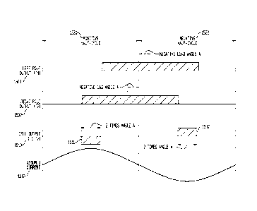
[0089] FIG. 20 illustrates a selective harmonic elimination (SHE) control
pattern according to various embodiments. In FIG. 20, the switching frequency
is
equal to twice the wanted frequency. The SHE control pattern of FIG. 20 is
nearly
identical to that of FIG. 7, except that a notch of duration angle B 2030 is
inserted into
the middle of the positive half-cycle 2020 of the left pole output Ti 2001,
and an
identical notch 2032 is also inserted into the middle of the negative half-
cycle 2022 of
the right pole output T2 2002. With these notches inserted, both the left pole
and the
right pole switch twice per cycle instead of once per cycle. The notches cause
the cell
output (Ti ¨ T2) 2010 to contain two pulses in each half-cycle instead of only
one
pulse. The duration and location of these two pulses are determined both by
angle A
2035 and by angle B 2030/2032, so that there are two degrees of freedom.
[0090] If the SHE waveforms of FIG. 20 were used in the cells of FIG. 1,
causing them to switch twice per cycle, it would be possible to obtain six
degrees of
freedom with only three cells per phase. This could permit the same number of
harmonics to be eliminated as was previously described for six cells per
phase, each
switching once per cycle. Such an approach might be a favorable tradeoff for
many
applications that could tolerate the higher switching frequency, and would
still give
lower switching losses than with PWM control.
[0091] FIG. 21 illustrates a selective harmonic elimination (SHE) control
pattern according to various embodiments. The SHE control pattern of FIG. 21
is
CA 02726056 2010-11-26
WO 2009/148555
PCT/US2009/003311
nearly identical to that of FIG. 20, except that the waveforms of the left
pole Ti 2101
and the right pole T2 2012 have been exchanged. The cell output (Ti ¨ T2) 2110
still
contains two pulses in each half-cycle instead of only one pulse, but these
pulses have
the opposite polarity compared to FIG. 20. Thus, the SHE method associated
with
FIG. 21 can produce negative power flow.
[0092] Solutions for the SHE angles may not necessarily exist for all possible
values of fundamental (wanted) voltage. FIG. 22 shows the results of two
searches,
when the computer program was configured to eliminate four harmonics (the 5th,
7th,
11th, and 13th.
) utilizing three power cells per phase group. One continuous solution
was found between 62% and 0% fundamental voltage, and a second was found
between 69% and 62% voltage. These were combined to create FIG. 22.
[0093] The angles A-F in FIG. 22 are interpreted as follows: Each cell
produces two pulses symmetrically located in each half-cycle. These two pulses
can
be visualized as one main pulse with a narrower notch in the middle. A notch
can be
visualized as a pulse of negative width. The first of the three power cells
produces a
main pulse of width 2*D, with a notch having width -2*A. The second of the
three
power cells produces a main pulse of width 2*E, with a notch having width -
2*B. The
third of the three power cells produces a main pulse of width 2*F, with a
notch having
width -2*C. Because the notch width angles must be negative, there are more
constraints than in the searches associated with FIG. 9. Due to the additional
constraints, whereas the solutions of FIG. 9 reached a maximum voltage of 87%,
the
solutions of FIG. 22 only reached a maximum voltage of 69%. If the notch width
exceeds the main pulse width, the cell will produce negative pulses during the
positive
half-cycle, and will have negative power flow.
26
CA 02726056 2010-11-26
WO 2009/148555
PCT/US2009/003311
[0094] For better clarity, the waveforms are displayed for the angles A-F
plotted in FIG. 22, for two specific values of fundamental voltage. These two
specific
values are indicated by dotted vertical arrows in FIG. 22, and respectively
correspond
to FIGs. 23 -26. Each of FIGs. 23-26 list a value for "M" (which is
proportional to the
desired fundamental amplitude), lists the value (in degrees) of the six
respective angles
A-F, illustrate the output voltages of the three cells (CLal, CLa2, CLa3) in
the A
phase-group of a power supply according to various embodiments, illustrate the
sum
of the cell voltages in the A, B and C phase groups, and illustrates the
control variable
Q which controls the rotation of the angle commands. Each of FIGs. 23-26 also
shows
the load voltage from phase A to neutral, and the assumed load current for
phase A.
[0095] FIG. 23 shows the waveforms corresponding to 13% of maximum
possible fundamental voltage, with no angle command rotation. The output of
each A-
group cell repeats for each cycle without change, and is different from the
other A-
group cells. As shown in FIG. 23, the power cell CLal is producing positive
pulses
during the positive half cycle. The power cell CLa2 is also producing positive
pulses
during the positive half cycle, but of a different duration than those of
power cell
CLal. The power cell CLa3 is producing negative pulses during the positive
half-
cycle, and will have negative power flow. Thus, each of the power cells is
producing a
different amount of power. The bottom portion of FIG. 23 shows the waveforms
of
the slim of the output voltage 2310 from all cells, and the assumed waveform
of the
output current 2312.
[0096] FIG. 24 also shows the waveforms corresponding to 13% of maximum
possible fundamental voltage, but with angle command rotation. The variable Q
steps
through three successive values during the three-cycle rotation interval, and
then the
27
CA 02726056 2010-11-26
WO 2009/148555
PCT/US2009/003311
pattern repeats. The steps occur at the end of each full-cycle, and because
all the poles
have the same values at those points, the rotation will not cause extra
switching events.
The value of Q is used to determine which SHE waveform is assigned to each
cell.
The load voltage 2410 from phase A to neutral (Van) in FIG. 24 is the same as
in FIG.
23, because as previously stated it does not matter which cell is assigned to
implement
each individual angle command.
[0097] FIG. 24 shows that with angle command rotation every full-cycle, each
cell produces the same waveform during the three-cycle rotation period (with a
one-
cycle phase shift between cells). Each cell experiences one cycle of negative
power
flow, but the average power for each cell is positive, and is the same for all
cells.
[0098] FIG. 25 shows the waveforms corresponding to 69% of maximum
possible fundamental voltage, with no angle command rotation. The output of
each A-
group cell repeats for each cycle without change, and is different from the
other A-
group cells. As shown in FIG. 25, the power cell CLa I is producing positive
pulses
during the positive half cycle. The power cell CLa2 is also producing positive
pulses
during the positive half cycle, but of a different duration than those of
power cell
CLal. The power cell CLa3 is also producing positive pulses during the
positive half
cycle, but of a different duration than those of power cells CLa I and CLa2.
Thus,
each of the power cells is producing a different amount of power.
[0099] FIG. 26 also shows the waveforms corresponding to 69% of maximum
possible fundamental voltage, but with angle command rotation. The variable Q
steps
through three successive values during the three-cycle rotation interval, and
then the
pattern repeats. The steps occur at the end of each full-cycle, and because
all the poles
have the same values at those points, the rotation will not cause extra
switching events.
28
CA 02726056 2010-11-26
WO 2009/148555
PCT/US2009/003311
The value of Q is used to determine which SHE waveform is assigned to each
cell.
The load voltage 2610 from phase A to neutral in FIG. 26 is the same as in
FIG. 25,
because as previously stated it does not matter which cell is assigned to
implement
each individual angle command.
[00100]FIG. 26 shows that with angle command rotation every full-cycle, each
cell produces the same waveform during the three-cycle rotation period (with a
one-
cycle phase shift between cells). The average power for each cell is positive,
and is
the same for all cells.
[00101] As described hereinabove, SHE waveforms that provide more than one
degree of freedom per cell may be utilized to control the fundamental
amplitude of the
output voltage and to eliminate harmonics. FIG. 27 illustrates a selective
harmonic
elimination (SHE) control pattern which has three degrees of freedom, and also
a
switching frequency equal to three times the wanted frequency. This pattern is
similar
to the pattern of FIG. 7, where the left pole output Ti 2701 is advanced by an
angle A
while the right pole output T2 2702 is retarded by the same angle A. However,
in FIG.
27, a notch of duration angle C and a pulse of duration angle B are inserted
into the
positive half-cycle 2720 of the left pole output Ti 2701. The negative half-
cycle 2722
of the left pole output Ti 2701 is the same with opposite polarity, so that it
contains a
notch of duration angle B and a pulse of duration angle C. The right-pole
output T2
2702 is also similar to that shown in FIG. 7, except that a notch of duration
angle C
and a pulse of duration angle B are inserted into the negative half-cycle 2722
of the
right pole output T2 2702. The positive half-cycle 2720 of the right pole
output T2
2702 is the same with opposite polarity, so that it contains a notch of
duration angle B
and a pulse of duration angle C.
29
CA 02726056 2010-11-26
WO 2009/148555
PCT/US2009/003311
[00102] With these notches and pulses inserted, both the left pole and the
right
pole switch three times per cycle instead of once per cycle. The notches and
pulses
cause the cell output (Ti ¨ T2) 2710 to contain three pulses in each half-
cycle instead
of only one pulse. The duration and location of these three pulses are
determined by
angle A, angle B, and angle C; so that there are three degrees of freedom.
[00103] If the SHE waveforms of FIG. 27 were used in the cells of a power
supply similar to FIG. 1, causing them to switch three times per cycle, it
would be
possible to obtain six degrees of freedom with only two cells per phase. This
could
permit the same number of harmonics to be eliminated as was previously
described for
six cells per phase, each switching once per cycle. Such an approach might be
a
favorable tradeoff for many applications that could tolerate the higher
switching
frequency, and would still have lower switching losses than PWM control.
[00104] FIG. 28 illustrates a SHE control pattern which has a switching
frequency equal to three times the wanted frequency. This pattern is nearly
identical
to the control pattern of FIG. 27, except that the waveforms of the left pole
Ti 2701
and the right pole T2 2702 have been exchanged. The cell output 2710 is also
nearly
identical to that of FIG. 27, except that the polarity is reversed, so that
the cell now
produces negative voltage during the positive half- cycle 2720, and positive
voltage
during the negative half-cycle 2722. Thus, the SHE control pattern of FIG. 28
can be
utilized to produce negative power flow.
[00105] For the waveforms of FIGs. 27 and 28, the process of finding SHE
angles that give a desired fundamental voltage while eliminating certain
harmonic
voltages would be similar to the cases previously shown, for patterns that
switch once
per cycle and twice per cycle.
CA 02726056 2010-11-26
WO 2009/148555
PCT/US2009/003311
[00106] According to various embodiments, SHE waveforms may be utilized to
switch the devices in a high-speed motor drive once per cycle. Then as speed
(and
hence frequency) is reduced, at about one-half of top speed, other SHE
waveforms
may be utilized to switch the devices twice per cycle. The switching losses
would still
be no worse than at top speed, but twice as many harmonics could be
eliminated. As
speed is reduced further, at about one-third of top speed, yet other SHE
waveforms
may be utilized to switch the devices three times per cycle. The switching
losses
would still be no worse than at top speed, but three times as many harmonics
could be
eliminated. This process may be continued further and further as the speed is
reduced.
Eventually, the speed may reach a point where it becomes acceptable to utilize
PWM
control to switch the devices.
[00107] FIG. 29 illustrates an exemplary control system 2900 for controlling a
high-speed AC motor 2905 using the methods described herein. Referring to FIG.
29,
a power circuit 2910 is controlled by a system that measures current 2921 and
voltage
2923 signals between the power circuit 2910 and rotating motor frame 2905. The
measured three-phase current and voltage signals each may be transformed to a
two-
phase representation (2922, 2924), and to a representation that estimates
voltage and
current in the rotating d-q axis (2926, 2928). A flux estimator 2930 may use
the d-q
voltage current to determine the stator flux amplitude, frequencies and phase.
[00108] The flux speed regulators 2932, 2934 are used to generate current
commands for the flux and torque producing components, 2936, 2938
respectively.
The current regulators 2940 regulate the measured d-q currents to the
commanded
values. Feed-forward signals 2942, 2944 are added to decouple the flux and
torque,
and to improve transient response.
31
CA 02726056 2016-02-22
54106-616
[00109] With this control method, slip compensation 2950 may be used, but
typically only for induction motors. For synchronous and permanent magnet
motors,
in which the rotor spins at the same frequency as the stator, the slip
compensation
block 2950 may not provide any output. All other functions are the same.
Stator
resistance is the parameter that primarily affects the stability of stator
flux based
control. An incorrect value of rotor resistance may cause speed error only,
and may
not affect the torque. The problem of stability at low speeds may be addressed
by
using a robust motor voltage integrator (not shown) to estimate stator flux.
[00110] The embodiments described herein may be used in various
applications, including high speed applications (e.g., frequencies of 250
hertz and
greater), at medium voltage (2300 volts and higher) and high power (e.g., 1000
kilowatts and higher).
[00111] While several embodiments of the invention have been described
herein by way of example, those skilled in the art will appreciate that
various
modifications, alterations, and adaptions to the described embodiments may be
realized
without departing from the scope of the invention defined by the appended
claims.
32