Note: Descriptions are shown in the official language in which they were submitted.
CA 02726601 2010-12-31
-1-
RF ADAPTER FOR HELD DEVICE VVITII VARIABLE VOLTAGE
DROP
BACKGROUND OF TDB INVENTION
The present invention relates to industrial process control or monitoring
systems. More specifically, the present invention relates to field devices in
such
systems which are Capable of Radio Frequency (RF) communication:.
In industrial settings, control systems are used to monitor and control
inventories of industrial and chemical processes, and the like. Typically, the
=
to control system performs these functions using field devices
distributed at key
locations in the industrial process and coupled to the control circuitry in
the
control room by. a process control loop. The term "field device" refers to any
device that performs a function in a distributed control or process monitoring
system, including all devices currently known, or yet to be 'mown, used in the
measurement, control and monitoring of industrial processes. . *
Some field devices include a transducer. A transducer is understood to
mean either a device that generates an output signal based on a physical input
or
that generates a physical output based on an input signal. Typically, a
transducer
transforms an input into an output having a different form. Types of
transducers
include various analytical equipment, pressure sensors, thermistors,
thermocouples, stain gauges, flow transmitters, positioners, actuators,
solenoids, indicator lights, and others.
Typically, each field device also includes communication circuitry that is
used for communicating with a process control room, or other circuitry, over a
process control loop. In some installations, the process control loop is also
used
to deliver a regulated current and/or voltage to the field device for powering
the
field device. The process control loop also carries data, either in an analog
or
digital format.
Traditionally, analog field devices have been connected to the control
room by two-wire process control current loops, with each device connected to
CA 02726601 2010-12-01
WO 2009/154756
PCT/US2009/003636
-2-
the control room by a single two-wire control loop. Typically, a voltage
differential is maintained between the two-wires within a range of voltages
from
12-45 volts for analog mode and 9-50 volts for digital mode. Some analog field
devices transmit a signal to the control room by modulating the current
running
through the current loop to a current proportional to the sensed process
variable.
Other analog field devices can perform an action under the control of the
control
room by controlling the magnitude of the current through the loop. In addition
to, or in the alternative, the process control loop can carry digital signals
used
for communication with field devices.
to In some
installations, wireless technologies have begun to be used to
communicate with field devices. For example, completely wireless installations
are used in which the field device uses a battery, solar cell, or other
technique to
obtain power without any sort of wired connection. However, the majority of
field devices are hardwired to a process control room and do not use wireless
communication techniques. Further, in many field installations, "intrinsic
safety" standards must be implemented which limit the amount of stored energy
which can be discharged into the environment.
In some configurations, an RF adapter can be connected in series with
the process control loop. In such a configuration, the voltage drop across
terminals of the adapter may affect operation of the process control loop.
Further, the amount of this voltage drop affects the maximum power available
to
the adapter for use in operation of circuitry of the adapter.
SUMMARY OF THE INVENTION
A wireless adapter for use in a two-wire process control loop includes
wireless communication circuitry and first and second terminals configured to
couple in series with the two-wire process control loop. A regulator having a
regulator input is coupled to the first terminal and an output. Shunt
circuitry is
coupled to the output of the regulator and is configured to provide power to
the
wireless communication circuitry. A feedback circuit is configured to control
CA 02726601 2015-10-13
- 3 -
current flowing from the regulator to the shunt circuitry as a function of a
loop current
flowing through the two-wire process control loop.
According to an aspect of the present invention there is provided a wireless
adapter for use in a two-wire process control loop configured to couple to a
process field
device in an industrial process control system coupled to the two-wire process
control
loop and provide wireless communication to the process field device, the
wireless
adapter comprising:
wireless communication circuitry;
first and second loop terminals configured to couple in series with the two-
wire
process control loop and a process variable transmitter, the first and second
loop
terminals carrying a loop current therebetween, the loop current powering the
wireless
adapter and carrying information;
a switching regulator having a switching regulator input coupled to the first
loop
terminal and an output;
a shunt circuitry coupled to the output of the switching regulator and
configured
to provide power to the wireless communication circuitry; and
a feedback circuit configured to control current flowing from the switching
regulator to the shunt circuitry as a function of the loop current flowing
through the two-
wire process control loop as measured through at least one of the first and
second loop
terminals, wherein the feedback circuit is configured to control a voltage
drop across the
first and second loop terminals.
According to another aspect of the present invention there is provided a
method
of providing wireless communication to a process field device coupled to a two-
wire
process control loop using a wireless adapter, the method comprising:
coupling first and second loop terminals of the wireless adapter to the two-
wire
process control loop and in series with a process variable transmitter, the
first and
second loop terminals carrying a loop current therebetween, the loop current
powering
the wireless adapter and carrying information;
generating a regulated output with a regulator in the wireless adapter coupled
to
the first loop terminal;
providing power to wireless communication circuitry in the wireless adapter
using shunt circuitry which is coupled to the regulated output of the
regulator and
thereby providing power to the wireless communication circuitry;
communicating wirelessly using the wireless communication circuitry; and
CA 02726601 2015-10-13
- 3a -
adjusting current flowing from the regulator to the shunt circuitry as a
function
of the loop current flowing through the two-wire process control loop as
measured
through at least one of the first and second loop terminals and thereby
controlling a
voltage drop across the first and second loop terminals.
BRIEF DESCRIPTION OF THE DRAWINGS
Figure 1 is a simplified diagram showing an industrial process control or
monitoring system which includes field devices having wireless adapters.
Figure 2 is a cross-sectional view of a field device of Figure 1 including a
wireless adapter.
Figure 3 is a wiring diagram showing a field device and wireless adapter
coupled to a two-wire process control loop.
Figure 4 shows an example configuration of a variable voltage drop circuit for
coupling to a two-wire process control loop.
Figure 5 shows another example embodiment of a variable voltage drop circuit
including a microcontroller.
Figure 6 is another example configuration of a variable drop circuit including
a
microcontroller having a feedback.
Figure 7 is a simplified circuit diagram of a variable voltage drop circuit
having
another example configuration.
Figure 8 is a schematic diagram of a variable voltage drop circuit including a
switch for switching between a variable and a fixed voltage drop mode.
Figure 9 is a simplified block diagram showing components of a wireless
adapter having a variable voltage drop circuit.
DETAILED DESCRIPTION OF ILLUSTRATIVE EMBODIMENTS
The present invention provides a wireless adapter for use with a field device
in
an industrial process control or monitoring system. The wireless adapter
couples to the
field device and provides the field device with wireless communication
abilities. The
adapter also couples to a two-wire process control loop which is used to a
local location such as a
CA 02726601 2010-12-01
WO 2009/154756
PCT/US2009/003636
-4-
process control room or the like. The adapter has a power supply arrangement
which allows the voltage drop across terminals of the adapter to vary.
Figure 1 is a simplified block diagram of a process control and
monitoring system 10. In Figure 1, field device 12 is shown coupled to process
piping 14 which carries a process fluid 16. In this example, the field device
12 is
illustrated as being a process variable transmitter. For example, a process
variable transmitter may measure a process variable of process piping 14 such
as pressure, flow rate, temperature, etc. Other types of field devices include
control devices which are used to control operation of industrial process 10.
However, the present invention is not limited to such a device. Field device
12 is
typically located at a remote location, for example in a field of an
industrial
process plant and couples to a local location, such as a control room 20
through
a two-wire process control loop 22. Control room 20 includes a load resistance
20A and a power source 20B. The two-wire process control loop 22 can operate
in accordance with any appropriate standard or technique. A typical
communications standard includes 4-20 mA process control loops in which a
process variable is represented by a current level flowing through the process
control loop. Another example includes digital communication techniques which
may be modulated onto the analog current level of the two-wire loop, for
example HART communication standard. Other purely digital techniques are
also employed including FieldBus based protocols. Typically, the field device
12 is powered using power received over the process control loop 22.
In Figure 1, a wireless adapter 30 is shown coupled to the field device
12. Wireless adapter 30 can be used for wireless communications, illustrated
by
arrows 32 and 34 with other devices. For example, the adapter 30 can
communicate with a handheld communicator 40 or another field device 42
which includes a wireless adapter 44. Field device 42 is shown coupled to
process piping 46.
CA 02726601 2010-12-01
WO 2009/154756
PCT/US2009/003636
-5-
The wireless adapter 30 can communicate to other devices or
components as desired. The communication can be in accordance with any
appropriate protocols. One example protocol includes the formation of a mesh
network in which data is passed between wireless devices in order to expand
and improve the reliability of the communication system
Figure 2 shows a simplified cross-sectional view of field device 12 and
wireless adapter 30 coupled to two-wire process control loop 22. In the
example
of a process variable transmitter, field device 12 includes a process variable
sensor 50 which is connected to measurement circuitry 52 configured to
to measure a process variable. Transmitter circuitry 54 is configured to
receive the
process variable and communicate the process variable onto the two-wire
process control loop 22 using known techniques. The transmitter 12 couples to
the two-wire process control loop through connection block 106. The wireless
adapter 30 also couples to connection block 106 and is mounted to the housing
of transmitter 12, for example, through threaded connections 122 and 109. For
example, the coupling is through an NPT conduit coupling 109. A similar
conduit connection 109 is also used to couple to conduit 111 which carries the
two-wire process control loop 22 therethrough. The chassis of the wireless
adapter 30 couples to an electrical ground connector 110 of transmitter 12
through wire 108. The transmitter 12 includes a two-wire process control
connection block 102 which couples to connection 112 from the wireless
adapter 30. A housing 120 of the wireless adi.Pter 30 carries an antenna 126
which couples to circuitry of the wireless adapter 30. An RF transparent end
cap
124 can be sealably coupled to the housing 120 to allow transmission of RF
signals therethrough. In the arrangements shown in Figure 2, five electrical
connections are provided to the RF adapter which include four loop connections
along with an electrical ground connection.
Figure 3 shows a simplified block diagram 150 which illustrates the
electrical connections between the control room 20, the field device 12 and
the
CA 02726601 2010-12-01
WO 2009/154756
PCT/US2009/003636
-6-
wireless adapter 30. As illustrated in Figure 3, the wireless adapter 30 is
coupled
in series with the process control loop 22 through the Loop+ (also identified
herein as L+) and Loop- (also identified herein as L-) connections and the
field
device 12 is also coupled in series with its plus power and minus power
connections. HART communication connection is used by the adapter 30 to
communicate on the process control loop 22.
During operation, the adapter 30 operates using current from the 4-20
mA current flowing through the process control loop 22. As current flows
through adapter 30, a small voltage drop occurs across its L+ and L- terminal
connections. Preferably, the amount of that voltage drop is kept sufficiently
small to ensure that there is enough voltage remaining in the process control
loop 22 to provide power to the field device 12. For example, the voltage that
the adapter drops may be on the order of 1.0 volts. The current in the process
control loop may be as low as 3.5 mA under some conditions, and as high as 25
mA under other conditions. Therefore, in such a configuration, the power
available to the adapter 30 may vary from 3.5 mA to 25 mA assuming a fixed
1.0 volt drop. Thus, the circuitry of the adapter 30 receives more operating
power when the loop is operating at higher current levels.
In Figure 3, the load resistor 20A is illustrated. Load resistor 20A is used
by the process control system to sense the current Ithop flowing through the
process control loop 22. For example, a process control system can convert a
measured voltage across the load resistance to a value which is indicative of
the
process variable being sensed by a process variable transmitter. This variable
may be related, for example, to process pressure, temperature, level, flow, or
some other measured parameter. Typically, the load resistance has a value of
250 ohms. When the process control loop is carrying 4 mA, the voltage across
this resistor is 1.0 volts. Similarly, when the process control loop is
operating at
20 mA, the voltage drop across the resistor is 5 volts. If the voltage drop of
the
process variable transmitter is relatively constant as the current in the loop
CA 02726601 2010-12-01
WO 2009/154756
PCT/US2009/003636
-7-
varies, there is more voltage available for the circuitry of adapter 30 when
the
control loop is operating at 4 mA than when the control loop is operating at
20
mA. The present invention provides a technique for varying the voltage drop
across the adapter whereby a greater voltage drop is available to the adapter
(and
more power is available to the adapter) when the current flowing through the
process control loop is at a low value. Similarly, less voltage drop is
provided
across the adapter when the loop is operating at a higher current level. In
this
way, the minimum power that the adapter 30 may obtain is raised and therefore
the performance in the circuitry can be improved, for example, to increase
wireless communication power.
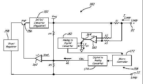
Figure 4 is a simplified schematic diagram of variable voltage drop
circuitry 150 in accordance with one example embodiment. Variable voltage
drop 150 includes a DC to DC switching converter or switching regulator 152
which is coupled to a shunt regulator 154 through a transistor 156. The input
of
regulator 152 couples to the process control loop 22 through a resistor RI.
The
input to regulator 152 is at a voltage level Vreg. The base of transistor 156
is
coupled to feedback circuitry 158 which comprises OpAmps 160 and 162,
transistor 164 and resistors R2, R3, R4 and R5.
The circuitry shown in Figure 4 senses the loop current using resistor R1
and varies the regulated voltage at the terminals L+ and L-. OpAmp 160
operates as a current sensing amplifier and creates a voltage drop across R3
that
is equal to the voltage drop across R1 by varying the current Is. The
relationship
between Is and the loop current is as follows:
koop * = Is * R3 Eq.!
= 'Loop * (R1/ R3) Eq. 2
Thus, the current Is is proportional to the loop current based upon the ratio
established by R1 and R3. Example values for R1 and R3 may be 1 ohm and 5000
CA 02726601 2010-12-01
WO 2009/154756
PCT/US2009/003636
-8-
ohms, respectively. In such a configuration, Is is equal to the loop current
divided by 5000.
OpAmp 162 operates to regulate the voltage drop across L+ and L-
_
terminals of the adapter by varying the current to the shunt regulator 154 by
maintaining the voltage on its inverting input equal to the voltage on its non-
inverting input. In Figure 4, the non-inverting input is coupled to a
reference
voltage \Tref, Vg is the value of the voltage across the loop terminals. The
reference voltage Vref can be established using any appropriate technique, for
example, using a band gap voltage reference. The inverting input of OpAmp 162
operates as a summing node into which current Is flows. As the voltage across
R5
is fixed, the current through R5 is also fixed. Therefore, as Is varies with
the loop
current, the current flowing through R4 varies in an equal but opposite
manner.
As Is increases with the loop current, the current through R4 decreases and
therefore Vreg, the voltage across the L+ and the L- decreases. This causes a
lower voltage drop across the terminals as the current in the process control
loop
22 increases. For example, the value of \Tin when the loop is operating at 4
mA
and 20 mA can be adjusted by changing the values of RI, R3, R4 and R5. If Ri
is
one ohm, R3 is 5000 ohms, R4 is 309 kohms, R5 is 39.1 kohms, and Vref=0.25
volts, then Vg will be 1.98 volts when the loop 22 is operating at 4 mA and
0.99 volts when the loop is operating at 20 mA.
One feature of the configuration shown in Figure 4 is that the circuitry
has a very fast response time. For example, the loop current may change from 4
to 20 mA in a relatively short period of time. It is important that if a
change
occurs, the voltage drop will change as quickly as possible. This is because
at 20
mA loop currents, the load resistor 20A "consumes" more of the loop voltage.
To ensure that the process device, such as a process variable transmitter,
always
has sufficient voltage for operation, the voltage drop across the adapter 30
must
change rapidly in response to changes in the loop current.
CA 02726601 2010-12-01
WO 2009/154756
PCT/US2009/003636
-9-
Figure 5 shows another example embodiment of variable voltage drop
circuitry 170 in which the voltage drop is controlled by a microprocessor 172.
Microprocessor 172 provides a digital value to digital to analog converter 174
which connects to the inverting terminal of OpAmp 162 through a resistor R6.
In
this configuration, the feedback circuitry 158 can operate in an open loop
configuration such that the current Is into the summing node of OpAmp 162 can
be varied as desired. Thus, the voltage drop across the L+ and L- terminals
can
be varied as desired. For example, Vreg can be set during manufacture and
modified during operation depending upon the voltage available to the adapter
circuitry in a particular process control loop 22. However, one drawback to
such
a configuration is that the voltage available for the adapter 30 must be
predetermined by either the manufacturer or operator. Further, this
configuration
does not take advantage of the fact that more voltage will be available to the
adapter 30 when the loop current is low than when the loop current is high.
Figure 6 shows another example configuration in which the micro
controller 172 receives a digital representation of the current ILoop flowing
through the process control loop 22. Note that similar elements have retained
their numbering. In Figure 6, an analog to digital converter 182 is arranged
to
sense a voltage drop across a resistor R7 which is proportional to the current
Is.
This value is digitized and provided to microcontroller 172. As discussed
above,
microcontroller 172 can then control the voltage across the L+ and L-
terminals
by controlling the digital to analog converter 174. One advantage of such
configuration is that the microcontroller 172 is able to receive information
related to the loop current and this information can be communicated, for
example using HART communication, to an operator over the process control
loop 22 or through the wireless interface. However, the additional analog to
digital and digital to analog converters, as well as the decreased speed of
the
system, provide disadvantages.
CA 02726601 2010-12-01
WO 2009/154756
PCT/US2009/003636
-10-
In the above circuitry configurations there are situations which may
cause the circuitry to reset. For example, if the circuitry is set such that
Vg is
approximately 2.25 volts when the lo_op current is operating at 3.5_ mA, and
decreases to approximately 1.0 volts when the loop current increases to 25 mA.
A failure in the loop may cause the loop current to increase beyond 25 mA. If
this happens, the voltage Vreg will continue to increase and approach the
value of
Vref which is coupled to OpAmp 162. If the DC to DC switching regulator 152
requires a voltage input which is greater than Vref for operation, the output
from
the DC to DC converter will decrease and potentially cause the microprocessor
or wireless communication circuitry in the adapter 30 to reset. If the
wireless
communication circuitry resets, the adapter 30 will disconnect from the
wireless
communication network and require a rejoining process once the circuitry is
stable. During such an occurrence, it is not possible to communicate
wirelessly
with the device. If a mesh network is employed, the network may need to
reconfigure itself. Further, the OpAmp 160 must be able to function with its
input terminals operating near the upper power supply voltage. For example,
the
supply voltage may be approximately 2.35 volts. It may be desired that the
voltage across the L+ and L- terminals may be as high as 2.5 volts. In such a
situation, the input terminals of OpAmp 160 may exceed the positive power
supply voltage.
Figure 7 is a schematic diagram of variable voltage drop circuitry 190
which is configured such that the circuitry does not cause the loop terminal
voltage to drop below the operating range of the switching regulator 152 and
does not require that the current sensing OpAmp be operated near its positive
power supply voltage. In Figure 7, similar elements have retained their
numbering. However, note that in Figure 7, R3 has a new location at the output
of OpAmp 160. Further, R1 is connected in series with the negative loop
terminal. In this configuration, OpAmp 160 creates an output voltage that is
proportional to the current flowing through RI. The varying voltage of this
CA 02726601 2010-12-01
WO 2009/154756
PCT/US2009/003636
-11-
output causes a varying current through resistor R3, which in turn causes an
equally varying current through resistor R4, This varying current through R4
causes Vreg to also change. The relationship between loop current and Vreg is
as
follows:
Ii oop * R1 = lb * Rb Eq. 3
ILoop=Ib*Rb/R1 Eq. 4
Vout = * RF + Ib * Rb Ithop * Rf Eq. 5
11::1 Now, substituting Equation 4 into Equation 5:
Vow = 'Loop * (R1/ Rb) * (Rf + Rb) + ILoop * Rf Eq. 6
Is = (Vout ¨ Vref) / R3 Eq. 7
Vreg = (Is + 15) * R4 + Vref Eq. 8
Equation 6 above shows that the output of OpAmp 160 (Voõt) is directly
proportional to the current flowing through the adapter, As koop
increases,
Is increases due to Vow increasing as shown in the relationships set forth in
Equation 7. As Is increases, the current flowing through R4 must decrease as
the
current flowing through R5 is constant because Vref is constant. As the
current
flowing R4 decreases, the voltage across R4 decreases and therefore Vreg
decreases. Thus, the equations illustrate that as the loop current increases
the
voltage across the adapter loop terminals (Vreg) decreases.
The circuitry of Figure 7 overcomes the first drawback discussed above
as the input terminals of OpAmp 160 operate slightly below the negative power
supply of voltage of the device. One example OpAmp is the LMP2231 available
from National Semiconductor which is capable of operating with its input
CA 02726601 2010-12-01
WO 2009/154756
PCT/US2009/003636
-12-
terminal voltages below the negative power supply voltage. The device can also
operate using a relatively low power supply voltage and supply current. The
device has a low input offset voltage as well as low input offset voltage
drift due
to ambient temperature changes.
If the resistor values of the circuitry shown in Figure 7 are selected
correctly, the second shortcoming discussed above can be overcome. As the
output Võt of OpAmp 160 saturates at or near the positive power supply
voltage, the resistors values may be selected such that when the loop current
reaches 25 mA, the output Vow can no longer increase. If the output of OpAmp
to 160 does not increase further, the value of Vreg will similarly decrease
no
further. Therefore, these circuits can be arranged such that Vreg reaches a
minimum value when ILoop reaches 25 mA which will not be exceeded. If Ii,op
increases beyond 25 mA, Vreg will maintain this minimum voltage and thus the
DC to DC converter 152 will always have sufficient voltage for operation. This
will ensure that the microprocessor and wireless communication circuitry of
the
adapter 30 will continue operating even if the loop current has an abnormally
high value.
Further, similar to some of the circuits discussed above, the circuit 190
shown in Figure 7 has a relatively fast response time. One additional
advantage
of the configuration shown in Figure 7 is that the circuitry may be easily
modified to provide a fixed voltage drop. Figure 8 shows an example variable
or
fixed voltage drop circuit 192. Circuit 192 is similar to circuit 190 shown in
Figure 7 except that a switch 194 is included in the path of current Is. When
switch 194 is opened, Is becomes zero and the voltage across R4 no longer
changes such that Vreg no longer changes. Thus, the circuit of Figure 8 is
switchable between a variable voltage drop circuit and a fixed voltage drop
circuit. One example switch which may be employed is the ADG842 available
from Analog Devices. This switch is normally closed so that the circuit
operates
normally in the variable voltage drop mode. The switch may be controlled by
CA 02726601 2010-12-01
WO 2009/154756
PCT/US2009/003636
-13-
the microcontroller in the adapter and changed upon receiving the appropriate
wired or wireless command.
Suitable values for the components shown in Figure 8 are as follows:
Table 1
Rf = resistance of fuse (-2 ohms)
R1 =5 ohms
Rb -= 12.1 kohms
RF = 232 kohms
R3 = 332 Kohms
R4 = 187 Kohms
R5 = 35.7 kohms
160= LMP2231 (National Semiconductor)
162 = TC1035 (Microchip Technology Inc.)
Vref = 0.34 volts
DC/DC converter = TPS61070 (Texas Instruments)
Figure 9 is a schematic diagram of circuitry of adapter 30 shown in block
diagram format including variable loop voltage drop circuitry 190. Adapter 30
includes a microprocessor 200 having an internal memory which is configured
to control operation of the device and communicate using, for example, the
HART communication protocol over the process control loop 22 using a
HART modem 202. A radio communication module 204 is provided for
wireless communications using an antenna 206. The microprocessor 200 is
powered by an LDO (Low Dropout Regulator) 210 which is coupled to the
output from DC to DC converter 152. A reset circuit 212 is provided to reset
microprocessor 200 should the voltage drop below a desired operating point. In
this configuration, the shunt regulator 154 is illustrated as a number of
CA 02726601 2010-12-01
WO 2009/154756
PCT/US2009/003636
-14-
components. A capacitor 214 is shown having a value of 10,000 uF which is
used to store power for use in operating radio module 204. A voltage
clamp/current shunt 216 is provided to set the maximum voltage across
capacitor 214. A DC to DC switching regulator 218 is used to provide a
regulated three volt output to LDO 220 which provides power to the radio
module 204. A reset circuit 222 is provided to reset the radio module 204 if
the
voltage drops below a desired threshold. A level shift circuit 226 is provided
for
coupling communication signals between the radio module 204 and the
microprocessor 200. HART modem 202 receives HART communication
signals from the HART connection using HART C0 receive circuit 230 and
transmits HART communication signals using HART transmit circuit 232.
These circuits are coupled to the HART terminal through a capacitor 234. In
Figure 9, a variable voltage network 240 is provided and couples between the +
Loop terminal and the output of OpAmp 160. The variable voltage network 240
comprises resistors R3, R4 and R5 shown in Figure 7. (Note that in this
simplified
illustration resistors Rb, Rf and RF are not shown).
The present invention provides a field device and/or adapter configured
to couple to a process control loop which further includes a wireless
communication module for one way or bi-directional wireless communication.
The wireless communication module can transmit and/or receive an RF signal
from a remote device or location. The module can be directly powered with
power received from the two-wire process control loop, or can be powered with
power received from the process control loop and stored for subsequent use.
The
module can be a removable module in which the module need only couple to
those field devices in which wireless communication is desired. The module can
be configured as an adapter to retrofit an existing transmitter.
The above configuration provides an adapter which enables
wireless communication with a process variable transmitter. The circuitry can
be
configured to operate from power which is already available to the process
CA 02726601 2010-12-01
WO 2009/154756
PCT/US2009/003636
-15-
variable transmitter. Increased efficiency can be obtained by placing the
energy
storage element as a shunt element in a loop shunt regulator. A "step up"
regulator can be provided which is part of the feedback circuit for the shunt
regulator control. This configuration increases efficiency while reducing the
number of components required. The voltage drop across the device can be
varied as desired.
The term "field device" as used herein can be any device which is
used in a process control monitoring system and does not necessarily require
placement in the "field." The device can be located anywhere in the process
control system including in a control room or control circuitry. The terminals
used to connect to the process control loop refer to any electrical connection
and
may not comprise physical or discrete terminals. Any appropriate radio
frequency communication circuitry can be used as desired as can any
appropriate communication protocol, frequency or communication technique.
The power supply circuitry is configured as desired and is not limited to the
configurations set forth herein. In some embodiments, the field device
includes
an address which can be included in any RF transmissions such that the device
can be identified. Similarly, such an address can be used to determine if a
received signal is intended for that particular device. However, in other
embodiments, no address is utilized and data is simply transmitted from the
wireless communication circuitry without any addressing information. In such a
configuration, if receipt of data is desired, any received data may not
include
addressing information. In some embodiments, this may be acceptable. In
others, other addressing techniques or identification techniques can be used
such
as assigning a particular frequency or communication protocol to a particular
device, assigning a particular time slot or period to a particular device or
other
techniques. Any appropriate communication protocol and/or networking
technique can be employed including token-based techniques in which a token is
CA 02726601 2013-10-01
-16-
handed off between devices to thereby allow transmission or reception for the
particular device.
Although the present invention has been described with reference to
preferred embodiments, workers skilled in the art will recognize that changes
may be made in form and detail without departing from the scope of
the invention. As used herein, Radio Frequency. (RF) can comprise electro-
magnetic transmissions of any frequency and is not limited to a particular
group
of frequencies, range of frequencies or any other limitation. Any
communication
protocol can be used, as desired, including IEEE 802.11b, 802.15.4, or other
to protocols, including proprietary protocols as well as standardized
protocols such
as the wireless HART communication protocol. In the discussion above, the
wireless adapter provides a digital signal communication connection for
coupling to the two-wire process control loop and, in some embodiments,
communicating in accordance with the HART communication protocol. The
is adapter can be configured to mount externally to a process control
transmitter,
for example, through a threaded coupling to NPT fittings in the transmitter
housing. In the above discussion, when a capacitor which is not a super
capacitor is employed, for example on the order of 10,000 AF is used to store
energy, the intrinsic safety circuitry of the present invention operates to
limit the
20 maximum available energy which is entering the circuitry of the adapter.
This is
because in accordance with intrinsic safety standard, the voltage across a
given
capacitance must be kept below a level that could result in the capacitance
creating a spark if an instantaneous short circuit occurred. Thus, in the
above
discussion, by limiting the maximuin circuit voltage which can be received by
25 circuitry in the adapter, the size of the capacitance can be increased.
As used
herein, "shunt regulator" is not limited to the particular configurations
shown
and may comprise any type of circuitry in the adapter in which current is
ultimately (and substantially) shunted back to the two-wire process control
loop.
More generally, this can comprise shunt circuitry which is used to power
CA 02726601 2013-10-01
-17-
wireless communication circuitry. Current flowing through the shunt circuitry
is returned
(shunted) to the two-wire process control loop. Although the present invention
has been
described with reference to preferred embodiments, workers skilled in the art
will
recognize that changes may be made in form and detail without departing from
the scope
of the invention.