Note: Descriptions are shown in the official language in which they were submitted.
CA 02726707 2011-01-14
- 1 -
RF ADAPI'gR FOR mix DE.vics -wITH LOW VOLTAGE
INTRINSIC SA.FXTY CLAMPING
BACKGROUND OF Tie INvENnoN
The present invention relates to industrial process control or
monitoring systems. More specifically, the present invention relates to ,field
devices in soch systems which am capable. of Rain Frequency (BF)
communication.
In industrial settings, control systemi are used to monitor and
to control inventories of industrial and chemical processes, and the like.
Typically,
the control system performs these functions using field devices distributed at
key locations in the industrial process and coupled to the control circuitry
in the
control room by a process control loop. The term "field device refers to any
device that petforms a. function in a distributed control or process
monitoring
15 system, including all devices enn-ently known, or yet to be ;mown, used
in the
measurement, control and monitoring of industrial processes.
Some field devices include a transducer. A transducer is
understood to mean either a device that generates an output signal based on.a
physical input or that generates a physical ontput based on an input signal.
20 Typically, a transducer transforms an input into an output having a
different.
form. Types of transducers include various analytical equipment, pressure
sensors, thentaistori,thennoomiples,' strain gauges, flow transmitters,
positioners, actuators, solenoids, indicator lights, and others,
Typically, each field device also includes communication
25 circuitry that is used for communicating with a process control room, or
other
circuity, over a process control loop. In some installations, the process
control
loop is also used to deliver a regulated current and/or voltage to the field
device
ibt powering the geld device. The process control loop also carries data,
either
in an analog or digital format,
Traditionally, analog field devices have been connected to the
control room by two-wire process control current loops, with each device
CA 02726707 2010-12-01
WO 2009/154748
PCT/US2009/003616
-2-
connected to the control room by a single two-wire control loop. Typically, a
voltage differential is maintained between the two wires within a range of
voltages from 12-45 volts for analog mode and 9-50 volts for digital mode.
Some analog field devices transmit a signal to the control room by modulating
the current running through the current loop to a current proportional to the
sensed process variable. Other analog field devices can perform an action
under
the control of the control room by controlling the magnitude of the current
through the loop. In addition to, or in the alternative, the process control
loop
can carry digital signals used for communication with field devices.
In some installations, wireless technologies have begun to be
used to communicate with field devices. For example, completely wireless
installations are used in which the field device uses a battery, solar cell,
or other
technique to obtain power without any sort of wired connection. However, the
majority of field devices are hardwired to a process control room and do not
use
wireless communication techniques. Further, in many field installations,
"intrinsic safety" standards must be implemented which limit the amount of
stored energy which can be discharged into the environment.
SUMMARY OF THE INVENTION
An adapter for coupling to a process control transmitter of the
type used to monitor a process variable in an industrial process includes a
first
connection configured to couple to a first side of a two wire process control
loop, a second connection configured to couple to a second side of the two
wire
process control loop and in series with a first connection to a process
control
transmitter, and a third connection configured to couple to a second
connection
of the process control transmitter. Wireless communication circuitry is
coupled
to at least the third connection and is configured to provide wireless
communication for the process control transmitter. Intrinsic safety circuitry
coupled to at least one of the first, second and third connections is
configured to
CA 02726707 2014-12-03
- 3 -
limit transfer of electrical energy to a value which is less than an intrinsic
safety value.
According to an aspect of the present invention, there is provided an adapter
for
coupling to a process control transmitter of a type used to monitor a process
variable in an
industrial process, the adapter comprising:
a first adapter connection configured to couple to a first wire of a two wire
process
control loop;
a second adapter connection configured to couple to a first transmitter
connection of
the process control transmitter;
a third adapter connection configured to couple to a second transmitter
connection of
the process control transmitter and to a second wire of the two wire process
control loop,
wherein the third adapter connection is used to communicate information on the
two wire
process control loop;
wireless communication circuitry configured to provide wireless communication
for
the process control transmitter, wherein the first and second adapter
connections are used to
power the wireless communication circuitry; and
intrinsic safety circuitry coupled to the first adapter connection, the second
adapter
connection, or the third adapter connection, or a combination thereof and
configured to limit
energy transfer to a value which is less than an intrinsic safety value;
wherein the two wire process control loop is used for powering the process
control
transmitter and powering the wireless communication circuitry, and the two
wire process
control loop is further configured to carry the information communicated from
the third
adapter connection.
According to another aspect of the present invention, there is provided a
method of
coupling a wireless adapter to a process control transmitter of a type used to
monitor a
process variable in an industrial process, the method comprising:
coupling a first adapter connection to a first wire of a two wire process
control loop;
coupling a second adapter connection to a first transmitter connection of the
process
control transmitter;
coupling a third adapter connection to a second transmitter connection of the
process
control transmitter;
powering wireless communication circuitry with power received from the two
wire
process control loop through the first and second adapter connections;
communicating information on the two wire process control loop using the third
adapter connection; and
CA 02726707 2014-12-03
limiting energy transfer through at least one of the first, second and third
adapter
connections to a value which is less than an intrinsic safety value, wherein
the two wire
process control loop is used for powering the process control transmitter and
powering the
wireless communication circuitry, and the two wire process control loop is
further
configured to carry the information communicated from the third adapter
connection.
BRIEF DESCRIPTION OF THE DRAWINGS
Figure 1 is a simplified block diagram of a process control monitoring system
including a field device configured for wireless communication.
Figure 2 is a block diagram of a process controller monitoring system in which
multiple field devices transmit information to a remote meter.
Figure 3 is an exploded cut away view of a field device including wireless
communication circuitry for communicating with a remote device such as a hand
held unit.
Figure 4 is a diagram of a process controller monitoring system which includes
a
field device for wireless communication which scavenges power from the process
control
loop.
Figure 5 is a more detailed schematic diagram of circuitry shown in Figure 4.
Figure 6 is a graph of voltage versus time as measured across a capacitor
shown in
Figure 5.
Figure 7 is an electrical block diagram of circuitry for providing wireless
communications in a process controller monitoring system.
Figures 8A and 8B are block diagrams showing a wireless communication adapter
coupled to a process variable transmitter through a two wire process control
loop.
Figure 9 is a simplified block diagram showing circuitry of a wireless
communication adapter.
Figure 10 is a simplified cross-sectional view showing a wireless adapter
coupled to
a transmitter.
Figure 11 is a simplified diagram showing a process control loop including an
intrinsic safety barrier.
CA 02726707 2010-12-01
WO 2009/154748
PCT/US2009/003616
-4-
Figure 12 is a simplified schematic diagram showing a wireless
adapter including intrinsic safety circuitry.
Figure 13 is a more detailed schematic diagram of the wireless
adapter of Figure 12.
Figure 14 is a simplified schematic diagram showing intrinsic
safety circuitry showing active circuitry.
Figure 15 is a simplified schematic diagram showing the wireless
adapter using active intrinsic safety circuitry.
Figure 16 is a more detailed schematic diagram of the wireless
adapter of Figure 15.
DETAILED DESCRIPTION OF ILLUSTRATIVE EMBODIMENTS
The present invention provides a field device and/or adapter
configured to couple to a process control loop which further includes a
wireless
communication module for one way or bi-directional wireless communication.
The wireless communication module can transmit and/or receive an RF signal
from a remote device or location. The module can be directly powered with
power received from the two-wire process control loop, or can be powered with
power received from the process control loop and stored for subsequent use.
The
module can be a removable module in which the module need only couple to
those field devices in which wireless communication is desired. The module can
be configured as an adapter to retrofit an existing transmitter. Circuitry is
provided for intrinsic safety protection.
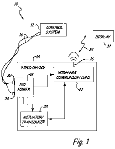
Figure 1 is a simplified block diagram of a process control or
monitoring system 10 in which a control room or control system 12 couples to a
field device 14 over a two-wire process control loop 16. The field device 14
includes I/0 power circuitry 18, actuator/transducer 20 and wireless
communication circuitry 22. The wireless communication circuitry 22 is
configured to send and/or receive an RF signal 24 using an antenna 26.
Currently, industrial instrumentation often includes a local
display or "meter" which can be used for local monitoring of process
= CA 02726707 2011-01-14
infintordion, The meter can be quite useful in many installations, however,
such
a local display configuration does have several limitations. A local display
requires direct visual aeons to the field device. Further, typically an
operator
can only viewa single meter at a time. The instruroents which contain the
meter
are often not at a convenient location or viewing angle. One technique which
has
been used to address such a configuration is the use of a meta whfch is wired
to
a process transmitter. This allows the meter to be mohmed at a more convenient
location. Another technique is shown and described in U.S. patent application
Serial No. 10/128,769, filed April 22, 2002, entitled PROCPSS
)0 TRANSMITTER WITH WIRELESS COMMUNICATION LINK, and
which has matured to U.S. Patent 6,839,546.
With the present invention, an RE communication module is
included in a field device, or configured as ao adapter to retrofit a field
device
which can be used in additionto the connection to a process control loop such
as
Is loop 16. The wireless ccaranunieation module 22 can be
configured to be
compact and lower power such that it on be easily included in existing field
device configurations. The module can be used for wireless transmission of
information for use in monitoring control anti/or display of data. Such a
radio
transmitter can make the field device information available in a local area.
For
20 example, a shigle local 'display such as display 32 ean be
provided and used to
display information from the field device 14. The display 32 can be configured
to display information from several devices, either simultaneously,
sequentially,
or through commands provided to the display, for example using a manual input
such as buttons available to an operator. The display 32 can be placed at a
fixed
25 location or can be a portable device such that it can be carried
throughout the
process control system to monitor and observe operation of various field
devices. Depending on the strength of the RE signal 24 and the sensitivity of
the
transmit and receive circuitry, the area covered by the RE transmisaion can be
controlled as desired. For example, Figure 2 is a simplified diagram of a
process
so control system 50 in vvlaich a !amber of field devices 14 are
coupled to the
control room 12 through individual process control loops 16. Each field device
CA 02726707 2010-12-01
WO 2009/154748
PCT/US2009/003616
-6-
14 transmits an RF signal 24 for receipt by display 32. In this example,
display
32 is capable of displaying four process variables (PV1, PV2, PV3 and PV4)
which are received from the field devices 14 using antenna 52. As mentioned
above, the display 32 can be a fixed display or can be a portable display,
such as
a hand held unit. In this particular configuration, the display 32 is
illustrated as
showing two process variables which relate to process pressure and two process
variables which relate to process temperature. This allows the field devices
14 to
provide information over the RF connection within a desired range, for
example,
within a local area. For example, if the display 32 is within 40 meters of a
,field
device 14, it will be capable of receiving and displaying information from
that
field device. An optional user input 48 can be used to, for example, select
the
format of the display, the process variable displayed, or used to interrogate
a
field device 14.
Figure 3 is a simplified cutaway partially exploded view of a
pressure transmitter 60 which is one example of a field device. Pressure
transmitter 60 couples to two-wire process control loop 16 and includes a
transmitter housing 62. Process control loop 16 couples to terminals 56
carried
on terminal board 58. A pressure sensor 64 provides one example of a
transducer and is configured to couple to a process fitting to measure a
differential pressure occurring in a process fluid. The output from the sensor
64
is provided to measurement circuitry 66 which couples to field device circuit
68.
The field device circuit 68 implements aspects of the I/0 power supply 18
shown in Figure 1. The wireless communication circuitry 22 couples to field
device circuit 68 and may, in some embodiments, couple to process control loop
16.
The housing 62 includes end caps 70 and 72 which can be
screwed into the housing 62. End cap 72 includes an RF transparent window 74
configured to align generally with an antenna 26 carried on wireless
communication circuit 22. When attached, the end caps provide a intrinsically
safe enclosure for circuitry within transmitter 60. The materials typically
used in
CA 02726707 2010-12-01
WO 2009/154748
PCT/US2009/003616
-7-
end caps, for example metal, are not transparent to RF signals. However, RF
transparent window 74 allows RF signals to be sent from or received by antenna
26. One example RF transparent material for use with window 74 is glass or the
like. However, any appropriate material can be used. The window and housing
configuration can help to meet intrinsic safety requirements and provide flame
proof (explosion proof) capability. Further, the cavity within housing 62 can
be
configured to provide a desired radiation pattern of RF signals generated by
antenna 26. For example, it may be desirable to have the RF transmission be
directional in some implementations, or omnidirectional in others. In other
implementations, the cover 62 can be lengthened to provide an additional
interior cavity for placement of wireless communication circuit 22.
The wireless communication circuitry 22 can be selected as
desired. One example circuit is the "I-Bean" transmitter device available from
Millennial Net. However, other circuitry can be used. Analog or digital
signals
carried on process control loop 16 can be read and transmitted using the
wireless
communication circuit 22 without disrupting operation of the process control
loop 16 or field device circuitry 68. The circuitry used for wireless
transmission
should be sufficiently small and low powered to fit within the physical and
power constraints of process field devices. Some prior art transmitters are
configured to receive an optional display arranged generally in the position
shown for wireless communication circuit 22 in Figure 3. In such a
configuration, the wireless communication circuit 22 can be used in place of
the
local display. In such a configuration, the communication wireless circuitry
22
simply transmits an RF signal which couples directly to the process control
loop
16 and transmits an RF signal which corresponds to any analog and/or digital
signals carried on the loop 16.
In general, the process control loop discussed herein can
comprise any type of process control loop for use in industrial process
control
and monitoring systems. Such loops include 4-20mA current loops in which a
analog current level is varied between 4 and 20mA to transmit information. The
CA 02726707 2010-12-01
WO 2009/154748
PCT/US2009/003616
-8-
same control loop can be used to provide power to the field device. Another
type of process control loop is in accordance with the HART communication
protocol in which digital transmissions are superimposed on the 4-20mA signal
for transmission of additional information. Another example two-wire process
control loop uses a protocol set forth by the Instrument Society of America
(ISA) which is called the Field Bus SP50 protocol. However, end signaling
protocol can be used. Some process control loops are configured to connect to
multiple field devices such that the field devices can communicate with one
another or monitor transmissions from another field device. In general, any
type
of information transmitted on such process control loops, or available or
generated internally or received by a field device, or otherwise used to
control a
field device or other type of information, can be transmitted using the
wireless
communication techniques of the present invention. In another example, a hand
held unit or device used to configure field devices can be carried into the
field
by an operator. The operator uses the hand held device to send or receive
information to a field device when the hand held device is within proximity of
the field device. This allows the operator to gather information or program a
field device without having to physically couple to the device or the physical
process control loop.
In some embodiments, it is also desirable for communications
from a field device, or to a field device, to carry addressing information.
The
addressing information can be indicative of the source of the transmission or
the
intended recipient of the transmission. The wireless communication circuitry
can
transmit continuously or on a periodic or intermittent basis, as desired. In
another example, the wireless communication circuitry only transmits when
activated or "polled". The activation can be from a source internal to the
field
device, received through the process control loop, received from a wireless
source, or received or generated by another source. In environments in which
multiple field devices may transmit simultaneously, the transmission protocol
should be selected to avoid or address any type of collisions which might
CA 02726707 2010-12-01
WO 2009/154748
PCT/US2009/003616
-9-
interfere with the transmissions. For example, different frequencies or
frequency
skipping techniques can be used, random or semi-random transmission windows
can be used, repeated transmissions or token based techniques can be
implemented or other collision avoidance techniques as desired. If the
transmission includes error detection or correction information, this
information
can be used to detect an error in the transmission and/or correct any errors
in the
transmissions. If an error is not correctable, the receiving unit can request
a re-
transmission of the corrupt data or, can indicate an error, or can wait for a
subsequent transmission of the data, or take other steps as desired.
Figure 3 also shows an example hand held device 80 for
communication with circuitry 22 over RF connection 82. Hand held device 80
includes a display 84 and user input 86. Other types of inputs and outputs can
be
included in hand held device 80. Preferably, the hand held device 80 is
battery
operated and can be carried into the field by an operator for communication
with
field device 60. Information from the field device 60, or from other sources,
is
displayed on display 84 and the hand held device is controlled using input 86.
Commands or other information can be transmitted by the hand held device 80
to field device 60.
In one configuration, the wireless communication circuitry
requires power which is within the power constraints available in the field
device. For example, one display currently used within field devices uses 3.6
volts at 0.5 mA. If a transmitter which is capable of operating an LCD meter
is
employed, the wireless communication circuitry can replace the LCD meter and
use the same power source that is used to drive the LCD meter. In another
example, the wireless communication circuitry is powered directly from the
process control loop, for example using the voltage developed across a diode
drop connected in series with the process control loop. In embodiments in
which
no battery is used with the communication circuitry, the circuitry can more
easily meet intrinsic safety or other safety approval requirements and provide
an
indefinite field life without battery replacement or maintenance. In
CA 02726707 2010-12-01
WO 2009/154748
PCT/US2009/003616
-10-
configurations in which the wireless configuration is only for sending
information, power requirements can be reduced. In another example, if a
greater transmission range is desired, a stationary device such as display 32
as
illustrated in Figure 1 can include an RF repeater for re-transmission of data
received from, or sent to, a field device. The RF repeater can be loop
powered,
or can derive its power from other sources. Further, once the RF data is
received, it can be reformatted for transmission over other medium, for
example
an Ethernet connection, into existing data transmission structures used within
process control systems, over an extended range RF communication link such as
a cell phone, or relaying using another technique.
Figure 4 is a simplified diagram of a process controller or
monitoring system 100 which illustrates another aspect of the present
invention.
In system 100, a field device 14 connects to a control system 12 through
process
control loop 16 through junction box 102. In the embodiment of Figure 4, a
field
device 104 couples to the process control loop 16 and includes wireless
communication circuitry 122. The wireless communication circuitry 122 is
configured to send an RF signal 106 and to be completely powered by power
received from the process control loop 16.
Process device 104 includes a power regulator 110, a shunt or
bypass 112, and a super capacitor 114. During operation, the super capacitor
114 =
is slowly charged (trickle charged) using a power regulator 110 by using
excess
voltage tapped from the process control loop 16. The bypass 112 allows loop 16
to operate normally and is connected in series with loop 16. Communication
circuit 122 includes circuitry for receiving analog and/or digital information
carried on process control loop 16. The circuit 122 can responsively transmit
an
RF signal 106 based upon the received information. If operated as a receiver,
circuitry 122 is capable of modulating data onto the electrical current
carried in
the loop 16. This can be either analog or digital information. This
configuration
allows data to be relayed over a wireless communication network. The network
can be configured in accordance with any type of topology, including point to
CA 02726707 2010-12-01
WO 2009/154748
PCT/US2009/003616
-11-
point, spoke and hub and mesh topologies. Process device 104 can be positioned
at any location along the loop including configured as an individual device
such
as that illustrated in Figure 4. In some installations, the field device 104
should
be field hardened and configured for intrinsically safe operation. The device
104
can also be positioned within another field device 14, as part of a junction
box
102, or even located within the control room which houses control system 12.
The field device 104 can connect to more than one RF circuit 122 and/or more
than one process control loop 16, either simultaneously or through the use of
multiplexers or other techniques.
The use of a super capacitor allows the device to operate without
internal batteries or other techniques. The use of a capacitor allows quick
charging and the storage of sufficiently large energy potentials. When used in
a
hazardous environment, large energy storage may not be acceptable in order to
meet intrinsic safety standards. However, the process device 104 can be moved
away from the hazardous environment, such as at the junction box 102, where
intrinsic safety is not required.
Figure 5 is a simplified schematic diagram of field device 104
showing super capacitor 114 in greater detail. In this example, super
capacitor
114 comprises two 10 Farad capacitors configured to each carry a 2.5 volt
potential. This yields an equivalent capacitance of 5 farads with a 5 volt
potential drop. Assuming that the wireless communication circuit 122 is
capable
of operating at a voltage of between 4 and 5 volts, the available energy from
each of the 5 Farad capacitors is Y2*C(Vi2-VF2) which is 'A*5*(52_42)=22.51
Figure 6 is a graph of voltage versus time measured across super
capacitor 114. In this example, 600mW wireless transmitter which transmits a
burst signal for a period of td of 1 second will require 0.6J/S*1s=0.6J of
energy.
Thus, there is ample energy available for operation of such a communication
circuit 122.
A typical power supply used to provide power to a process
control loop provides 24 volts DC. However, in a 4-20mA system, a transmitter
CA 02726707 2010-12-01
WO 2009/154748
PCT/US2009/003616
-12-
may only require 12 volts to operate. Wiring losses in the process control
loop
may cause 2 to 4 volts of voltage drop. Assuming only 5 volts is available for
charging the super capacitor 114, and that the process control loop is
operating
at a low current level (i.e., 4mA), there is still 20mW available to charge
the
super capacitor 114. Because only 0.6J was consumed during the transmit cycle,
the available 20mW will charge the super capacitor to full capacity in a time
tc=0.6J/0.02W=30s. Therefore, such a configuration will be capable of
transmitting a signal having a 1 second duration every 30 seconds. Assuming
that the bandwidth of the communications signal is 200Kb/s and a packet size
of
200b, the burst time is reduced to one millisecond and the resulting transmit
time is 0.03 seconds. In such a configuration, diagnostic data can easily be
transmitted because it is not of a time critical nature. However, if
sufficiently
fast charge times are available, control and process variable signals can also
be
transmitted wirelessly.
Although a super capacitor is described, any energy storage
device can be employed including a battery, or other. The energy that is used
to
charge the storage device can be electrical or magnetic and can be derived or
collected from any source.
Figure 7 is a simplified diagram of process controller monitoring
system 150 which includes a control room 152 coupled to a field device 154
through two-wire process control loop 156. Process control loop 156 extends
across an intrinsic safety barrier 158. The control room 152 is modeled as
including a power supply 160 and a load resistance 162.
The field device 154 can be of any configuration and is not
limited to the specific schematic shown in Figure 7. RF communication
circuitry
170 is shown coupled in series with loop 156. Circuitry 170 can be implemented
in a terminal block of a field device. For example, circuitry 170 can be
configured as an add on module such that the two-wire process control loop 156
can connect to existing transmitter circuitry.
CA 02726707 2010-12-01
WO 2009/154748
PCT/US2009/003616
-13-
In the configuration illustrated in Figure 7, the communication
circuitry 170 enables wireless communication abilities to be added to a new or
existing process control loop or field device. The circuitry is configured to
be
powered by the process control loop and can be installed anywhere in the loop
ranging from the control room, anywhere along the loop itself, in the
intrinsic
safety (IS) barrier or junction box 158, as a stand alone field device, or
included
in another field device. The circuitry can be configured for any type of
communication. However, in one simple configuration, the circuit 170 is
configured to measure the current carried in process control loop 156 and
transmit an output related to the measured current to a wireless receiver.
Turning now to one specific embodiment of circuitry 170 shown
in Figure 7, a sense resistance 180 and a power supply diode 182 couple in
series with process control loop 156. The sense resistance 180 can be, for
example, 10 ohms and is used in sensing the current level I carried in the
process
control loop 156. A test diode 184 is also coupled in series with the loop 156
and provides a test point 186. This can be used to calibrate or characterize a
field
device coupled to circuitry 170. An intrinsic safety protection circuit 190 is
provided which includes diode 192 connected as shown across diode 182 and
isolation resistors 194 connected at opposed ends of sense resistance 180.
Diode
182 is part of a power supply 196 which includes capacitor 198, input filter
200,
regulator 202, capacitor 204 and secondary filter 206. Secondary filter 206
includes capacitor 208 and resistor 210. The power supply circuitry 196
generates a power supply voltage VDD relative to a circuit ground for use by
circuitry in measuring the loop current and wirelessly transmitting a
resultant
signal. Although a specific power supply implementation is shown, any
appropriate power supply configuration or embodiment may be used as desired.
In this embodiment, input circuitry 218 includes sense resistance
180 and is configured to measure the current I flowing through loop 156. Input
circuitry 218 also includes a filter 220 which provides a differential
connection
to an OP amp 222. The OP amp provides an amplified input signal to an analog
CA 02726707 2010-12-01
WO 2009/154748
PCT/US2009/003616
-14-
to digital converter 226 which is illustrated as part of a microprocessor 224.
A
clock circuit 228 is provided and used to provide a clock signal to, for
example,
microprocessor 224. Optional HARD? transmit and receive circuit 230 connects
to microprocessor 224, loop 156, clock circuit 228 and an RF transmit/receive
circuit 232. The optional HARTS circuit 230 is configured to receive a digital
chip select signal (CS1) from microprocessor 224. The RF circuit 232 is
configured to receive a separate digital chip select signal (CS2) from
microprocessor 224. Both the HARTS circuit 230 and the RF circuit 232 are
configured to communicate with the microprocessor 224 on an SCI bus,
depending on which chip select is active. Microprocessor 224 is also
configured
to provide a shut down signal to operational amplifier 222. Microprocessor 224
includes a memory 236 which is used for storing programming instructions,
temporary and permanent variables and other information and may include both
volatile and non-volatile memory. The memory can include, for example, an
EEPROM and can contain addressing information which uniquely identifies
circuitry 170. RF circuit 232 couples to an antenna 240 which can be
configured
as an internal antenna, external antenna, or combination, as desired.
Circuitry
170 is configured to couple across the two-wire process control loop 156 such
that the loop 156 can terminate at another field device such as a process
transmitter or process controller.
The circuitry 170 illustrated in Figure 7 can be implemented on a
single printed circuit board such that RF antenna 240 is formed integral with
the
board. This configuration allows the circuitry 170 to be easily implemented in
existing field devices and does not require the use of an external antenna.
This
reduces installation complexity.
The optional HARTS transmit/receive circuit 230 can be used to
monitor digital signals, such as a process variable, carried on the process
control
loop 156. Based upon the sensed digital signal, the HARTS circuitry 230 can
control operation of the RF transmit/receive circuit 232 for transmission of
information related to the sensed process variable, or other information. If
the
CA 02726707 2010-12-01
WO 2009/154748
PCT/US2009/003616
-15-
HARTS circuitry is implemented in accordance with the complete HARTS
protocol and appropriate RF protocol stacks, the circuitry can implement
gateway level functionality which will allow a HARTS master to communicate
in a bi-directional manner through the RF HARTS gateway device with a
HARTS capable field device on the process control loop 156. This allows
wireless communication with a field device for monitoring, configuration,
diagnostics, or exchange of other information or data.
Frequently, in process control or monitoring installations, an
operator is required to physically access a field device or the process
control
loop in order to exchange information with the field device. This allows the
operator to repair equipment and do preventive maintenance on the equipment.
The wireless communication configuration set forth herein allows the operator
to interrogate field devices which may be in locations which are difficult to
access. Further, even in configurations in which the field devices are easily
accessible, the wireless communication circuitry does not require an operator
to
remove covers on equipment such as transmitters or junction boxes in order to
expose loop wiring for physical connection to the process control loop. This
can
be particularly beneficial in hazardous locations where explosive gases or
vapors
may be present. A digital or analog process variable can be sensed by the
wireless communication circuitry and transmitted to a wireless meter or hand
held device as discussed above.
During operation, circuit 170 is placed in series with the process
control loop 156 where it utilizes the 4-20mA current flowing through the loop
to power itself. For field devices that employ a common electrical ground,
circuitry 170 can be inserted on the high voltage side of the loop connection.
This configuration allows access to other bus circuitry within the field
device
such as a CAN interface. The configuration includes a test connection 186 for
use in measuring loop current during testing. The sense resistance 180 is
preferably configured to provide an equivalent capacitance of zero as measured
at terminals 181 which connect to loop 156 in accordance with intrinsic safety
CA 02726707 2010-12-01
WO 2009/154748
PCT/US2009/003616
-16-
standards. Circuitry 170 is configured for nominal operation at between 3 and
4
volts and the zener diode 182 along with sense resistance 180 sets this
operating
voltage. The excess voltage available on typical 4-20mA current loop is
sufficient to operate circuitry 170. Further, power management techniques can
be employed to limit the current drawn from the loop to about 3mA. This allows
any field device connected to the process control loop to send an alarm level
signal of 3.6mA without collapsing the circuit by drawing more than the
available current level.
Zener diode 182 acts as a shunt element which is placed in series
with the loop 156 to develop a preregulated voltage on the input filter stage.
Any
portion of the loop current which is not used by circuitry 170 is shunted
through
zener diode 182. The input filter 200 can comprise capacitive, inductive and
resistive elements and is used to isolate the loop from any noise or load
fluctuation generated by circuitry 170. This also suppresses noise in the HART
extended frequency band in order to conform with HART standards.
The voltage regulator 202 can be any appropriate voltage
regulator such as, but not limited to linear or switch mode regulators and is
used
to supply the voltage VDD to the circuitry. Filter 206 is used to store energy
and
further decouples circuit loads from the regulator 202. The output voltage of
the
secondary filter 206 is allowed to sag by several hundred millivolts during
circuit load changes. This allows peak current draws by the circuitry 172 to
be
averaged from the 4-20mA current loop.
In this embodiment, the microprocessor 224 including A/D
converter, along with the RF circuitry 232 and input circuitry 218 can be
placed
into a sleep mode or low power mode during periods of idle operation in order
to reduce power drain. For example, at a selected interval such as every 10
seconds, an internal timer in the microprocessor can enable the measurement of
the loop current by the A/D converter. The measurement circuitry is allowed to
settle before the A/D conversion occurs. After the A/D conversion is
completed,
both the loop measurement circuitry and the A/D converter are turned off to
CA 02726707 2010-12-01
WO 2009/154748
PCT/US2009/003616
-17-
conserve power. The microprocessor passes the measured value to the RF
circuitry 232 for transmission. Upon completion of the transmission, the
microprocessor and RF circuitry return to the low power mode until the next
cycle. The microprocessor may even put itself to sleep temporarily to save
power. Using these power management techniques, the microprocessor is able to
manage overall current requirements of the circuit by staggering the load
demands on the regulator stage.
Loop current measurement is achieved using the 10 ohm sense
resistor 180 coupled in series with the 4-20mA current loop 156 to measure the
analog current level. The voltage developed across the sense resistor 180 is
filtered to remove fluctuations due to HART digital communications as well as
any loop noise. An operational amplifier stage 222 provides further signal
conditioning and the signal is passed to the AJD converter 226 of
microprocessor 224.
The RF circuitry 232 can be any appropriate circuitry or
configuration as desired. In one simple form, the RF circuitry 232 simply
transmits a measured variable to a wireless receiver. The antenna 240 can be
used to broadcast the RF signal and can be formed integral with the circuitry
170, for example in the form of traces routed around an outside edge of a
circuit
board. The RF circuitry 232 can, in some embodiments, include a wireless
receiver such that the circuitry 232 can be configured as a transceiver. The
same
antenna 240 can be used for both transmission and reception if desired. A
typical
low powered transceiver may have a communication range of about 200 feet,
however other ranges can be achieved using different power requirements,
circuit sensitivity, antenna configuration, and the like. If the circuitry 170
is
mounted in a metal enclosure, such as a field housing compartment of a
transmitter, an RF transparent portion of the housing should be used to allow
transmission and reception of signals from antenna 240. For example, as
discussed above, a glass window can be used. Other example materials include
CA 02726707 2010-12-01
WO 2009/154748
PCT/US2009/003616
-18-
any material which is sufficiently transmissive to RF signals including
plastic, or
other materials.
The addition of the optional HART circuitry 230 allows the circuitry
170 to selectively listen to a HART message on the 4-20mA signal carried on
the current loop 156. Information such as measured process variables,
diagnostic
information, or other information can be transmitted to a wireless receiver.
Further, if the HART circuitry 230 is configured to modulate a digital signal
onto the process control loop, it can be used to remotely command or
interrogate
a field device coupled to the loop 156. For example, the HART circuitry 230
can be configured to act as a secondary master on the 4-20mA current loop.
This, in conjunction with RF circuitry 232 configured as a full transceiver,
enables bi- directional communication and configuration of field device from a
wireless master unit, for example a hand held device 80 shown in Figure 3.
Microprocessor 224 can also preferably be used to implement
diagnostics functionality. Microprocessor 224 is configured to monitor the
voltage and current characteristics of the process control loop 156, improper
or
problematic variations in current and voltage can be identified using
diagnostic
techniques and can be transmitted to a remote location, either wirelessly, or
using the HART transmission capabilities provided by circuitry 230, or by
setting the current level carried on loop 156 to an alarm value or other pre-
determined value.
Circuitry 170 is preferably configured to allow operation in
hazardous locations and to meet the appropriate approval and specifications,
such as intrinsic safety standards. For example, the intrinsic safety
protection
190, along with intrinsically safety rated resistor 180 is used on the input
to the
circuitry 170. Using appropriate components and circuit layout, the addition
of a
redundant zener diode 192 in parallel with zener 182 provides a level of
redundancy and limits the amount of voltage that can enter this circuit in an
intrinsic safety protected system. Similarly, the sense resistor 180 can be
used to
limit the maximum current that can enter the circuit 170 and snub any
discharge
CA 02726707 2010-12-01
WO 2009/154748
PCT/US2009/003616
-19-
of stored energy from the circuit through its external terminals. This
provides an
equivalent capacitance of substantially zero. The loop measurement circuitry
is
further protected by two intrinsic safety rated high value resistors 194
connected
between the two ends of the sense resistor 180 and the filter 220. Other
circuit
components can be protected from any outside energy sources by the use of
potting material or the like which also prevents hazardous gases and vapors
from
reaching any internal storage elements and nodes in the circuitry 170. For
other
non-hazardous locations, intrinsic safety components may not be required.
There are a growing number of applications in industrial process
plants that utilize the benefits of wireless communications in process
transmitters. These transmitters may be monitoring process temperature,
pressure, level, or flow. Reasons for providing wireless communications to
these
devices include the cost savings of installing hundreds or even thousands of
feet
of wire or to ease the task of "connecting" to and communicating with the
process transmitter. For a wired communications system, any host whether it be
a process control system, or a portable handheld communicator, must physically
connect to wires that are connected to the process transmitter in order to
communicate with it. In contrast, with a wireless communications system, the
host may wirelessly "connect" to a desired process transmitter from any
location
in the process plant within communication range. Further, in a wired system,
the
user must remove the cover from the device in order to gain access to the
terminals for connecting a handheld communicator to perform diagnostics or
commissioning of the process transmitter. Removing the cover may require the
user to take several safety precautions to ensure that the safety features of
the
process transmitter, or the facility, are not compromised. Further, removing
the
cover from a process transmitter may require special work procedures, or even
process or partial plant shutdowns, if the transmitter is used in a
potentially
hazardous area in the process plant. A process transmitter with wireless
communications capability does not require the removal of the cover, and the
CA 02726707 2010-12-01
WO 2009/154748
PCT/US2009/003616
-20-
related procedures, in order to communicate either locally or from a distant
location.
There are a large number of installed process transmitters that
have "wired" HART ID communications capability. In some instances, it may be
desirable to add wireless communications capability to these devices without
having the expense of purchasing and installing a new process transmitter with
wireless communications built in. Preferably the device interfaces the
existing
HART enabled process transmitter to a wireless network. This device can act
as a communications translator, communicating via HART to the existing
process transmitters, and communicating over a wireless network to a wireless
host or other remote monitoring or diagnostic system. Further, it is
preferable
that another power source for this communications module is not required. The
module should operate from the same power that is already provided to the
process transmitter, while not negatively impacting the power available for
the
process transmitter. This communication device may operate from solar power,
but that is not practical in many installations. It may also operate off a
battery.
However, batteries have special safety drawbacks when used in process plants
adding to their expense, and also require periodic replacement, making them
undesirable.
Since process transmitters may be scattered across a process
plant, it is convenient for the users if they can communicate on a wireless
mesh
network. A mesh network is one in which each wireless device may serve as a
router for the other wireless devices. This ensures that each device in the
network has the most reliable communications path back to the host. These
communication paths are established when the network is initially established,
as well as whenever a new device joins the network. In many instances, it may
be desirable that a process control transmitter which is coupled to a two-wire
process control loop be also able to communicate information on a wireless
network. It may also be desirable that the device function as a router in a
"mesh
network." Further, in many instances it is preferable that the device operate
CA 02726707 2010-12-01
WO 2009/154748
PCT/US2009/003616
-21-
using power from the process control loop rather than requiring a separate
source of power.
Figure 8A and 8B show two example wiring configurations for a
wireless adapter 300 in accordance with one example embodiment. Wireless
adapter 300 is shown coupled to a process control loop 302 which is powered by
a DC power supply 304. The loop is illustrated as including a load resistance
306 and also couples to a process variable transmitter 308. In Figures 8A and
8B, the wireless adapter 300 includes two loop connections (Loop+ and Loop-)
which connect in series with the process control loop 302. One of the loop
connections couples to the power supply 304 while the other loop connection
couples to a loop connection of the process transmitter 308. The wireless
adapter
300 includes a third connection (labeled HARTS) which couples to the other
loop connection of the process transmitter 308. In the configuration shown in
Figure 8A, the Loop- connection of adapter 300 couples to the plus connection
of transmitter 308 while the HART connection of adapter 300 couples to the
minus connection (labeled "Test+ or - Power") connection of transmitter 308.
The arrangement in Figure 8B is slightly different in which the Loop+
connection of the adapter 300 couples to the minus connection of transmitter
308 while the Loop- connection of adapter 300 couples to the power supply 304
and the HART connection couples to the plus connection of transmitter 308.
The adapter 300 is also illustrated with an antenna 310. In the configurations
of
Figures 8A and 8B, the adapter 300 is configured as a three terminal device
through which all of the loop current I flows. The separate HART connection
is used to provide digital communication on the two wire process control loop
302. Although the Figures are labeled HART , the adapter is not limited to
operating in accordance with the HART communication protocol and may use
any appropriate protocol including Fieldbus protocols.
The adapter 300 is powered using power received from the
process control loop 302. The loop 302 is also used to provide power to the
transmitter 308. In one configuration, the adapter 300 regulates its voltage
to a
CA 02726707 2010-12-01
WO 2009/154748
PCT/US2009/003616
-22-
small value, for example 1.0 volts, such that it will have a minimal impact on
the
process control loop 302. The adapter 300 operates using the current available
from the loop 302. For example, if the transmitter 308 sets the loop current
to a
value of 5 mA, the adapter 300 will operate on this 5 mA. If the voltage drop
across the adapter is 1 volt, a total of 5 mW will be used by the adapter 300.
In
the case of a typical process variable transmitter, the loop current is varied
between 4 mA and 20 mA based upon a measured process variable. Thus, the
minimum power available to the adapter 300 will be about 4 mW and the
maximum value available will be about 20 mW. The adapter 300 must utilize
this power to perform all desired functions, including, communications on the
loop 302 as well as wireless communications. A typical wireless radio may
require up to a 3 volt supply and draw between 15 mA and 50 mA during
communications (the specifics depend on many parameters related to the
wireless network). As this current draw does not occur at all times, it is
possible
for the adapter to store power until it is needed to support the wireless
communication. As discussed above, a super capacitor can be used to store
power. These are relatively inexpensive and have relatively long life times.
Super capacitors may supply current as high as 1 amp for short periods of time
and may therefore be used to power the wireless communication circuitry.
Figure 9 is a simplified block diagram of the adapter 300 which
shows various circuitry blocks. A super capacitor 320 is illustrated and the
device 300 is configured for HART communication as well as wireless
communication.
As illustrated in Figure 9, adapter 300 includes a microcontroller
340 which also includes a memory and a modem for communication. The
memory is used to store programming instructions, configuration data,
variables, etc. HART analog circuitry 342 is configured to couple to the
process variable transmitter 308 through a DC blocking capacitor 346. A radio
module 344 is provided to enable adapter 300 to communicate using RF
communication techniques. A regulator 348 is provided which is configured as a
= CA 02726707 2011-01-14
DC to DC converter. A current shunt eirrarit 350 is connected in parallel with
regulator 348 and includes a bypass transistor 352 controlled by a OP
anap.354,
OP amp 354 operates based upon a difference between a reference voltage (V)
and the voltage applied to the regulator348, Regulator 348 provides a 2.3 volt
S output to a low dropout (LDO) regulator 360. Low dropout
(IMO) regulator 360
provides a regulated 2 volt power supply output to the microprocessor. 340.
HART analog circuits 342, reset circuit 382 and ADC 380.
The current through bypass transistor 352 is used to charge the
super capacitor 320. The voltage across the super capacitor 320 is set using a
to voltage clamp 370. For example, the voltage clamp Gae. be
set to 2.2 volts.
Another DC to DC converter 372 is configured as a step up converter and
provides a regulated voltage output of 3 volts to a low dropout (LDO)
regulator
374. The output of low dropout (WO) regulator 374 is set to 2.8 volts and used
to provide regulated power to radio module 344.
is The microprocessor 340 is connected to a analog to digital
converter 380 which is used to monitor the voltage of super capacitor 320.
Nficroprocessor 340 is also connected to a reset circuit 382. Microprocessor
340
provides data to the radio module 344 through a level shifting circuit 384.
It is preferable that the circuitry be able to support the maximum
20 anazamt of wireless communication activity while dropping a
minimum amount
of voltage in the loop 301 Therefore, the adapter 300 is preferably configured
to
use power from the loop 302 in a very efficient manner. In one specific
configuration, this can be achieved by using a low power microcontroller 340,
for example, Texas Instruments MSP430F148 I and by using law power analog
2.1 circuit components. These components can be powered by a low
supply voltage
to also minimize the total circuit power oonsamptiort. Further, the
microcontroller 340 can be configured to enter a "sleep" mode if desired when
certain functions are not needed, for example communication functions. In the
configuration shown in Figure 9, a separate modem is not utnized. Instead, the
30 microcontroller 340 is used to provide modem functionality.
CA 02726707 2010-12-01
WO 2009/154748
PCT/US2009/003616
-24-
It is also preferable to provide the radio module 344 with a large
amount of power. This allows more frequent communication and increased
reliability. The additional power can be used to publish information from the
transmitter 308, allow the adapter 300 to be used as a router for other
process
transmitters, for example in a mesh network and allow higher transmit power to
be used. This can result in a more reliable mesh network, as the path from
another wireless device through the adapter 300 to a host may be more reliable
than the path which is directly from the device to the host.
In the embodiment of Figure 9, the radio module 344 is powered
by super capacitor 320. Therefore, in order to increase the power which is
provided to the radio module 344, it is preferable to increase the power
stored by
super capacitor 320. In the configuration of Figure 9, this is achieved by
arranging the super capacitor 320 as a shunt element for the regulator 348
which
regulates the voltage drop across the terminals which couple to loop 302 in
conjunction with OP amp 354 and shunt transistor 352. In Figure 9, the voltage
across the loop terminals which couple to the process control loop 302 is
regulated to one volt. This is achieved by adjusting the current going to the
super capacitor using OP amp 354 and shunt transistor 352. In this
configuration, regulator 348 operates in series with the loop 302 and is in
the
feedback loop formed by OP amp 354. In a less efficient configuration, a
separate one volt shunt regulator and super capacitor charging circuit may be
implemented. However, this requires additional components and additional
power to operate. In contrast, in the configuration set forth in Figure 9, any
loop
current which is not used by the circuitry of adapter 300 is directed into
shunt
capacitor 320 for increased efficiency. This results in the maximum amount of
power being available for radio module 344. The voltage clamp 370 determines
the voltage to which capacitor 320 is charged. Once the super capacitor 320
reaches the voltage set by the voltage clamp 370, the excess current flows
through clamp 370 rather than into capacitor 320.
CA 02726707 2010-12-01
WO 2009/154748
PCT/US2009/003616
-25-
DC to DC converter 348 is configured as a low power "step up"
switching regulator that operates with an input voltage of 1 volt. Regulator
348
increases the 1 volt input voltage to a sufficiently high voltage to power the
remaining circuitry. In the example of Figure 9, this is 2.3 volts. The
converter
can be a switched capacitor type converter, an inductor based boost converter,
a
transformer based converter or other appropriate configuration. The LDO
regulator 360 regulates the 2.3 volt output from regulator 348 to 2.0 volts
and
removes any switching noise from the regulator 348. The output from the LDO
regulator 360 is used to power the microprocessor 340, HART analog circuits
342, memory, reset circuitry 382, and analog to digital converter 380.
HARTS analog circuit block 342 can comprise, for example, a
carrier detect circuit, a receive circuit and a transmit circuit. Preferably,
these
circuits are configured to have low power requirements while maintaining
acceptable communications integrity. The memory in microprocessor 340 can be
used to store programming code and temporary variables. Timers which are
internal to microprocessor 340 can be used to provide a "software" modem
functionality. The memory of the microprocessor 340 may include internal flash
memory, RAM as well as EEPROM or other non volatile memory. The
microcontroller 340 can be configured to monitor the voltage access super
capacitor 320 using analog to digital converter 380 which provides a digital
output to microcontroller 340 representative of the capacitive voltage. If
desired,
the microcontroller 340 can be used to determine whether the capacitor has a
sufficient voltage to support radio transmission. Reset circuit 382 can be
used to
ensure that microcontroller 340 does not operate when the voltage is
insufficient. For example, the reset circuit 382 can be configured to reset,
or turn
on, the microcontroller 340 when the supply voltage from LDO regulator 360
reaches a sufficient voltage level. The circuitry can also be used to reset
the
microcontroller 340 if a power "glitch" occurs.
Radio module 344 operates on a stable voltage of 2.8 volts
provided by LDO regulator 374. As discussed above, if the super capacitor 320
CA 02726707 2010-12-01
WO 2009/154748
PCT/US2009/003616
-26-
is charged to 2.2 volts, the DC to DC converter regulator 372 steps up the
voltage to 3 volts. During use, the voltage on the super capacitor will
decrease
and the step up converter is needed. The LDO regulator 374 is used to provide
a
stable 2.8 volts to the radio module 344. Preferably, regulator 372 is
configured
to operate off a minimum voltage of about 1 volt up to a maximum voltage of
about 2.2 volts. In some configurations, microcontroller 340 is configured to
turn off circuitry of radio module 344 if the voltage on the super capacitor
320 is
less than 1 volt.
Microcontroller 340 can be configured to transmit information
wirelessly using the radio module 344 by communicating over digital
communication lines between the radio module 344 and the microcontroller 340.
As the microcontroller operates from a two volt power supply while the radio
operates from a 2.8 power supply, the digital communication lines between the
two components must be level shifted using level shifting circuitry 384. For
example, this can be performed using very low power level translator circuits
such as Texas Instruments SN74LVC2T45DCU.
In one configuration, the microcontroller 340 can be configured
to adjust the voltage drop across the loop terminals which couple to loop 302.
For example, an optional control line 341 from the microcontroller 340 can be
coupled to the inverting input of OP amp 354 of the shunt circuitry 350. In
such
a configuration, additional power may be made available to the radio by
increasing the loop voltage drop under appropriate conditions. Similarly, if
the
impact on the process control loop of the circuitry of adapter 300 needs to be
reduced, the voltage drop can be decreased. However, this will provide less
power to the radio module and other circuitry of adapter 300 and may degrade
performance.
Figure 10 is a cross-sectional view of one embodiment showing a
process control transmitter 400 coupled to a wireless adapter 300. Transmitter
400 includes a sensor 64 and measurement circuitry 66 as discussed above.
Measurement circuitry 66 couples to field device circuitry 68. Transmitter 400
CA 02726707 2010-12-01
WO 2009/154748
PCT/US2009/003616
-27-
couples to two wire process control loop 302 through a connection block 406
and the wireless adapter 300. Further, the wireless adapter 300 couples to the
housing of transmitter 400. In the example shown in Figure 10, the coupling is
through a NPT conduit connection 409. A similar conduit connection 409 is also
used to couple to conduit 411 for carrying the two wire process control loop
302
therethrough. The chassis of wireless adapter 300 couples to an electrical
ground
connection 410 of transmitter 400 through wire 408. The transmitter 400
includes a two wire process control loop connection block 402 which couples to
connections 412 from wireless adapter 300. As illustrated in Figure 10, the
wireless adapter 300 can be threadably received in conduit connection 409.
Housing 420 carries an antenna 426 to support circuitry of the wireless
adapter
300. Further, an RF transparent end cap 424 can be sealably coupled to housing
420 and allow transmission of RF signals therethrough. Note that in the
arrangement shown in Figure 10, five electrical connections are provided to
the
RF adapter 300. These include four loop connections as illustrated in either
Figures 8A or 8B, along with an electrical ground connection.
As discussed above, in some installations it is important for field
equipment such as a wireless adapter, to be intrinsically safe, that is, to be
able
to be operated in environments in which the atmosphere is flammable or
explosive. For example, circuitry in the device can be configured to limit the
amount of energy which the device is capable of storing and/or which the
device
is capable of discharging at any given time. As illustrated above, the
wireless
adapter is connected in series with a field device such as a process
transmitter or
control valve and operates using power drawn from the current flowing through
the two wire process control loop. A small voltage drop occurs across the
wireless adapter. This voltage drop may be as low as 1.0 volts. However, as
the
current flowing through the two wire process control loop may, in some
instances, be as low as 3.5 mA, the instantaneous power available may be as
low
as 3.5 mW. However, in some configurations, the wireless adapter may require
more power. For example, the device may require 60 mW of power (3 volts at
CA 02726707 2010-12-01
WO 2009/154748
PCT/US2009/003616
-28-
20 mA) in order to transmit a wireless message. Similarly, the power required
to
receive a wireless transmission may also exceed the instantaneous power which
is available from the process control loop. Thus, it is desirable that the
wireless
adapter be able to store power internally for use when there is insufficient
power
instantaneously available from the two wire process control loop. Typically,
the
time required for wireless communication, both transmission and reception, is
relatively short while the power available from the process control loop is
available from a continual basis. This energy can be stored in a capacitor for
subsequent use. A standard capacitor can be used or, in some configurations, a
to super capacitor having a capacitance greater than 0.22 F. However, a
field
device which is configured to store energy must contain circuitry to prevent
excessive discharge of such energy if the device is desired to operate in an
intrinsically safe manner. Although with a super capacitor, the amount of
energy
coming out of the device must be limited, even if the standard capacitor is
employed intrinsic safety requirements still require limitations on the amount
of
energy coming into the device. The voltage across a given capacitance must be
kept below a level that could result in the capacitance creating a spark if
the
capacitance underwent an instantaneous short circuit. Therefore, limiting the
maximum voltage which can be applied to the device allows larger capacitance
values to be used while still meeting intrinsic safety limitations.
Figure 11 is a simplified diagram similar to Figure 8A showing
the wireless adapter 300 coupled to a two wire process control loop 302. In
Figure 11, an intrinsic safety barrier 450 is shown as coupled to the two wire
process control loop 302. Intrinsic safety barrier 450 limits the voltage and
current which can be supplied to any field devices coupled to the loop from
power supply 304. Further, in such a configuration, the field device, such as
process transmitter 308 can be configured to limit the amount of energy which
can be stored within its circuitry. However, as a capacitor, or a super
capacitor is
capable of storing power, additional circuitry must be provided to ensure that
any power stored in adapter 300 cannot be discharged from the device. In
CA 02726707 2010-12-01
WO 2009/154748
PCT/US2009/003616
-29-
another words, in order for a device coupled to process control loop to
maintain
intrinsic safety, the device must be configured such that any power which it
can
add back into the loop is limited. This can be particularly problematic if the
device stores energy, for example, by using a capacitor.
In one aspect of the invention, circuitry is provided to limit the
amount of power which the wireless adapter 300 is capable of discharging back
into the process control loop 302 or elsewhere.
Figure 12 is a simplified block diagram showing wireless adapter
300 including one example configuration of intrinsic safety circuitry 460. In
the
to example of Figure 12, zener diodes 462 and 464 are provided which can
comprise, for example, zener diode having a 6.2 volt bias voltage coupled
across
the loop+ and loop¨ connections. A 5 ohm resistance 466 is coupled in series
with the two wire process control loop 302. Diodes 470 and 472 are coupled
across the loop+ connection and the HARD') connection to the field device 308.
Similarly, diodes 474 and 476 are coupled across the loop¨ connection and the
HART connection to the field device 308. Resistors 480 and 482, and
capacitors 484 and 486 are connected in series with the HART connection to
the field device 308. In one embodiment, resistor 480 has a value of 49.9
ohms,
resistance 482 has a value of 248 ohms, capacitor 484 has a value of 2.2 AF
and
capacitor 486 has a value of 2.2 F.
In order to ensure that the wireless adapter meets intrinsic safety
requirements, the intrinsic safety circuitry 460 is configured to limit the
voltage
and current that the circuitry within the adapter 300 is capable of applying
to the
two wire process control loop 302. This limiting must occur both under normal
operating conditions as well as during a fault. Further, the circuitry should
be
redundant and continue to operate as desired even if some of the circuitry
components should fail. In one specific configuration, it is preferable to
limit the
voltage to less than 1.5 volts and the current to less than 100 mA.
Zener diodes can be used as voltage limiters for the intrinsic
safety circuitry 460 and can be configured to conduct current only during a
fault
CA 02726707 2010-12-01
WO 2009/154748
PCT/US2009/003616
-30-
condition. In other words, the Zener voltage is selected to be slightly higher
than
the operating voltage of the circuitry. In this way, the Zener diodes do not
waste
power during normal circuitry operation. Thus, in order to limit the voltage
into
or out of the wireless adapter 300 to be less than 1.5 volts, the operating
voltage
of the wireless adapter electronics must be less than 1.5 volts.
In operation Zener diodes 462 and 464 operate to limit the
voltage which can applied between the loop + and loop ¨ terminals. Similarly,
diodes 470 and 472 operate to limit the voltage which can be introduced into
the
circuitry by the loop + and HART terminals. Diodes 474 and 476 limit the
voltage which can be introduced through the loop ¨ in HART terminals. If the
voltage applied across these terminals exceeds the thresholds of the diodes,
the
diodes will conduct and thereby limit the voltage value. However, during
normal
operating conditions, the diodes are not conducting and therefore will not
have
any affect on operation of the circuitry. The resistance which is added in
series
with the capacitance acts to reduce the amount of charge which can be
instantaneously removed from the capacitance, and therefore reduces the chance
that a capacitance may cause a spark. For a particular voltage level,
additional
capacitance may be used in circuitry if there is additional resistance in
series
with the capacitance. The larger the resistance, the larger that the
capacitance
may be. The resistance that is connected to the HART terminal also limits the
amount of current which can be provided from that terminal.
Figure 13 is a more detailed block diagram similar to Figure 9.
Some of the elements have retained their numbering. In Figure 13, the HART
analog circuit 342 is illustrated as two separate components, receive circuit
342A and transmit circuit 342B. The HART receive circuit 342A couples to
the HART connection through resistor 490 which can comprise, for example, a
10K ohm resistance. Further, the input to the differential amplifier 354 is
provided by variable voltage circuitry 492 and also couples to the Loop +
terminal through resistor 493. The variable voltage circuit 492 couples to the
CA 02726707 2010-12-01
WO 2009/154748
PCT/US2009/003616
-31-
Loop - connection through resister 494 which can comprise, for example, 12.1K
ohms.
In the circuitry discussed above, diodes, such as Zener diodes are
used to provide intrinsically safe circuitry. However, the Zener diodes are
generally rated at 3.3 volts or higher, which exceeds the desired limits for
intrinsic safety. One such technique which can be used to limit the voltages
to
less than 3.3 volts is to use active shunt regulators instead of Zener diodes.
These regulators can be set to limit the voltage to 1.24 volts without
requiring
any external resisters, or to higher voltages through the use of resisters in
the
circuitry. However, one drawback to using active shunt regulators is that they
are typically only rated to handle relatively small power levels, for example
0.20
to 0.25 watts. Therefore, the power that they dissipate must be limited
through
the use of a fuse or the like.
Figure 14 is a simplified schematic diagram showing wireless
adapter 300, and wireless adapter circuitry shown generally at 300A, which
includes three active shunt regulators 500A, 500B and 500C connected across
the loop+ and loop¨ terminals. A fuse 502 is connected in series with the loop
connection. The shunt regulators may comprise, for example, TLVH431
regulators available from Texas Instruments. In accordance with intrinsic
safety
principles, as the shunt regulators are active circuits, three shunt
regulators must
be provided for redundancy. The regulators are arranged so that they limit
both
the voltage that can be applied to the two wire process control loop 302 as
well
as the voltage which is applied to circuitry 300A.
However, one additional complicating factor in providing
intrinsic safety by limiting both voltage and current that the wireless
adapter 300
can place on the control loop is that the adapter 300 circuitry includes a
third
connection. This is the communication connection identified as the HART
connection in the description set forth herein. Intrinsic safety requirements
require that the voltage and current which the adapter 300 is capable of
outputting at any time be limited for any combination of its three terminals.
CA 02726707 2010-12-01
WO 2009/154748
PCT/US2009/003616
-32-
Therefore, active shunt regulators can also be used with the HART connection
as illustrated in Figure 15. As illustrated in Figure 15, two additional sets
of
active shunt regulators are required. Shunt regulators 510A, 510B and 510C are
connected between the loop+ terminal and the HART terminal. Similarly,
active shunt regulators 512A, 512B and 512C are connected between the loop¨
terminal and the HART terminal. A capacitor 514 and resistance 516 are
provided as discussed above.
Another method that may be used to limit the current that a
capacitor can place on to the process control loop is to insert an electrical
resistance at any path from the capacitor to the loop terminals. However, this
requires a resistance between the step up DC to DC converter 384 and the
capacitor to limit the current to 100 mA which will result in a very large
power
loss. Less power is lost if three voltage drop Schottky diodes are placed in
series
between the DC to DC converter in the capacitor. An example of such circuitry
is illustrated at Figure 16. In this configuration, the connection to the HART
terminal can be limited by using a sufficiently large resistance 518 and 520.
Three Schottky diodes 522A, 522B and 522C are used to couple the DC to DC
converter 384 to the circuitry of the wireless adapter 300. An example
Schottky
diode is an RV161M available from Rohm of Plano, Texas. Other potential
paths from the capacitor 320 to the terminals include high resistive elements
such as the connection through amplifier 354.
In the above discussion, capacitor 320 comprises a "regular"
capacitor having a capacitance of, for example, 10,000 .F. However, in some
configurations, it may be desirable to store additional energy. In such a
configuration, a "super capacitor" can be used which may have a capacitance of
0.1 Farads or more. If a super capacitor is used for capacitance 320,
alternative
configurations must be used to provide intrinsic safety. This is because the
maximum discharge from the circuitry must be limited. In general, the lower
value to which the voltage and current are limited, the less energy the
circuitry
will be capable of providing back into the process control loop. For example,
it
CA 02726707 2010-12-01
WO 2009/154748
PCT/US2009/003616
-33 -
is desirable to limit the voltage to 1.5 volts or less and the current to
100mA or
less.
The above configuration provides an adapter which enables
wireless communication with a process variable transmitter. The circuitry can
be
configured to operate from power which is already available to the process
variable transmitter. Increased efficiency can be obtained by placing the
energy
storage element as a shunt element in a loop shunt regulator. A "step up"
regulator can be provided which is part of the feedback circuit for the shunt
regulator control. This configuration increases efficiency while reducing the
number of components required.
The term "field device" as used herein can be any device which is
used in a process controller monitoring system and does not necessarily
require
placement in the "field." The device can be located anywhere in the process
control system including in a control room or control circuitry. The terminals
used to connect to the process control loop refer to any electrical connection
and
may not comprise physical or discrete terminals. Any appropriate radio
frequency communication circuitry can be used as desired as can any
appropriate communication protocol, frequency or communication technique.
The power supply circuitry is configured as desired and is not limited to the
configurations set forth herein. In some embodiments, the field device
includes
an address which can be included in any RF transmissions such that the device
can be identified. Similarly, such an address can be used to determine if a
received signal is intended for that particular device. However, in other
embodiments, no address is utilized and data is simply transmitted from the
wireless communication circuitry without any addressing information. In such a
configuration, if receipt of data is desired, any received data may not
include
addressing information. In some embodiments, this may be acceptable. In
others, other addressing techniques or identification techniques can be used
such
as assigning a particular frequency or communication protocol to a particular
device, assigning a particular time slot or period to a particular device or
other
CA 02726707 2010-12-01
WO 2009/154748
PCT/US2009/003616
-34-
techniques. Any appropriate communication protocol and/or networking
technique can be employed including token-based techniques in which a token is
handed off between devices to thereby allow transmission or reception for the
particular device.
Although the present invention has been described with reference
to preferred embodiments, workers skilled in the art will recognize that
changes
may be made in form and detail without departing from the spirit and scope of
the invention. As used herein, Radio Frequency (RF) can comprise electro-
magnetic transmissions of any frequency and is not limited to a particular
group
of frequencies, range of frequencies or any other limitation. Any
communication
protocol can be used, as desired, including IEEE 802.11b, 802.15.4, or other
protocols, including proprietary protocols as well as standardized protocols
such
as the wireless HART communication protocol. In the discussion above, the
wireless adapter provides a digital signal communication connection for
coupling to the two wire process control loop and, in some embodiments,
communicating in accordance with the HART communication protocol. This
connection is illustrated in Figures 8A and 8B as being a parallel connection
with the process variable transmitter and which does not carry substantial
loop
current. The power connection is illustrated as being in series with the
process
control loop. As used
herein, bypass circuitry includes the bypass
configurations shown in Figures 4 and 5, the shunt configurations shown in
Figures 7 and 9, or other circuitry. The adapter can be configured to mount
externally to a process control transmitter, for example, through a threaded
coupling to NPT fittings in the transmitter housing. In the above discussion,
when a capacitor which is not a super capacitor is employed, for example on
the
order of mow is used to store energy, the intrinsic safety circuitry of the
present invention operates to limit the maximum available energy which is
entering the circuitry of the adapter. This is because in accordance with
intrinsic
safety standard, the voltage across a given capacitance must be kept below a
level that could result in the capacitance creating a spark if an
instantaneous
CA 02726707 2010-12-01
WO 2009/154748
PCT/US2009/003616
-35-
short circuit occurred. Thus, in the above discussion, by limiting the maximum
circuit voltage which can be received by circuitry in the adapter, the size of
the
capacitance can be increased. However, for extremely large capacitance values,
i.e. "super capacitors", the capacitor must be treated as an energy storage
device.
In such configurations, the intrinsic safety circuitry of the present
invention
operates to limit the maximum amount of energy which can come out of the
adapter circuitry. In the above discussion, the maximum current and voltage
which can be produced by the adapter is limited to 1.24 volts and 100 mA.
Thus,
the intrinsic safety circuitry of the present invention operates in two
different
manners depending upon the size of the capacitance employed.