Note: Descriptions are shown in the official language in which they were submitted.
CA 02727111 2010-12-06
WO 2009/147436 PCT/GB2009/050618
ELECTRICAL RESISTANCE HEATING ELEMENTS
The present invention relates to electrical resistance heating elements, more
particularly to silicon carbide electrical heating elements.
Silicon carbide heating elements are well known in the field of electrical
heating
elements and electric furnaces. Conventional silicon carbide heating elements
comprise predominantly silicon carbide and may include some silicon, carbon,
and
other components in minor amounts. Conventionally, silicon carbide heating
elements
are in the form of solid rods, tubular rods, or helical cut tubular rods,
although other
forms such as strip elements are known. The present invention is not
restricted to a
particular shape of the elements.
Silicon carbide electrical heating elements comprise parts commonly known as
`cold
ends' and `hot zones' which are differentiated by their relative resistance to
electrical
current. There may be a single hot zone or more than one hot zone [for example
in
three phase elements (such as in GB 845496 and GB 1279478)].
A typical silicon carbide heating element has a single hot zone having a
relatively
high resistance per unit length, and at either end of the hot zone, cold ends
having a
relatively low resistance per unit length. This results in a majority of the
heat being
generated from the hot zones when a current is passed through the element. The
`cold
ends' by virtue of their relatively lower resistance generate less heat and
are used to
support the heating element in the furnace and to connect to an electrical
supply from
which the electrical energy is supplied to the hot zone.
In the claims and in the following description the term "silicon carbide
heating
element" should be taken as meaning (except where the context demands
otherwise) a
body comprising predominantly silicon carbide and comprising one or more hot
zones
and two or more cold ends.
Frequently, the cold ends comprise a metallised terminal end portion remote
from the
hot zone so to assist good electrical connectivity with the electrical supply.
1
CA 02727111 2010-12-06
WO 2009/147436 PCT/GB2009/050618
Conventionally, electrical connection to the cold ends is by flat aluminium
braids held
in compression around the circumference of the terminal end by a stainless
steel
clamp or clip. The cold ends in operation have a gradient of temperature along
their
length, from operating temperature of the hot zone where the cold ends join
the hot
zone, through to close to room temperature at the terminal ends.
One of the earliest heating element designs was in the form of a dumbbell
shaped
element in which the cold ends were made of the same material as the hot zone
but
having a larger cross section than the hot zone. Typically, the electrical
resistance per
io unit length ratio of the cold end to the hot zones for such heating
elements was about
3:1.
An alternative approach is, in effect, to wrap a dumbbell shaped element into
a single
or double helix. Such a geometry is obtained by helically cutting part of a
tubular rod.
is Typical rods of this type are Crusilite Type X elements and Globar SG (a
sngle
helix element) or SR (a double helix element) rods.
An alternative approach is to use lower resistivity materials to form the cold
ends and
higher resistivity material to form the hot zone. Known methods to produce the
lower
20 resistivity material include by impregnation of the pore structure of the
ends of a
silicon carbide body with silicon metal by a process known as siliconising.
GB513728 (The Carborundum Company) disclosed a joining technique in which
materials of different resistivity are bonded by applying a carbonaceous
cement at the
25 joint and heating so that excess silicon in the cold ends permeates to the
joint between
the cold ends and the hot zone thereby reacting with carbon in the cement to
form a
silicon carbide bond. By these methods, the electrical resistance per unit
length ratio
of the cold end to the hot zone can be increased to about 15:1.
30 JP2005149973 (Tokai Konetsu Kogyo KK) discussed alleged problems in
migration
of silicon from the cold ends to the hot zone, and disclosed the addition of
molybdenum disilicide to the material of the cold end to prevent this
migration and
improve the strength at the cold ends/hot zone interface. A five part
construction is
2
CA 02727111 2010-12-06
WO 2009/147436 PCT/GB2009/050618
revealed in which a hot zone of recrystallised silicon carbide is bracketed by
a
MoSi2/SiC composite and then a SiC/Si composite. This arrangement had as a
consequence lowering of the resistivity of the cold end, so improving
efficiency.
Whilst such techniques offer an increased electrical resistance ratio, the
increase in
cost of the raw materials, and the complexity of multiple joins in materials,
leads to
high cost.
With increasing environmental concern over global warming, and increasing
energy
prices, many energy intensive industries utilizing electrical heating furnaces
need to
reduce their energy usage by cost effective means.
Improvements such as improved insulation of the furnace to prevent excessive
heat
loss have played a major role in reducing the energy consumption. However,
little has
1s been done to improve the energy efficiency of the elements in a cost
effective manner.
The applicant has explored a number of approaches that separately, or in
combination,
provide a cost effective increase in resistance ratios, and hence decreased
energy use.
In a first approach, the present applicant looked to mitigate the above
problems based
on the realisation that the difference in electrical conductivity between (3-
silicon
carbide and a-silicon carbide can be used to reduce the resistivity of the
material of
the cold end, leading to a reduction in the resistance per unit of the cold
end, and
consequently a reduction in power consumption.
Of the many polymorphic forms of silicon carbide, the two of interest which
influence
the characteristics of heating element cold ends are a-silicon carbide (SiC
6H) which
has a hexagonal crystal structure and (3-silicon carbide (SiC 3C) which has a
face-
centred cubic structure.
Baumann "The Relationship of Alpha and Beta Silicon Carbide", Journal of the
Electrochemical Society, 1952 ISSN:0013-4651, discusses the formation of
silicon
carbide and noted that primary (i.e. first to form) silicon carbide was (3-
silicon carbide
at all temperatures studied.
3
CA 02727111 2010-12-06
WO 2009/147436 PCT/GB2009/050618
However Bauman noted that:-
" Beta SiC begins to transform monotropically to alpha SiC slowly at
2100 C. It changes to the alpha form rapidly and completely at
2400 C."
It is known that nitrogen acts as a dopant in silicon carbide that has the
effect of
reducing electrical resistivity.
Typical electrical resistivities of commonly produced heating element
materials
consisting of two polymorphic types of silicon carbide are summarised in Table
1
below, which shows that (3-silicon carbide has a much lower electrical
resistivity than
a-silicon carbide.
Typically hot zones are formed from either recrystallised silicon carbide
which has
the characteristics of being a compact self-bonded silicon carbide matrix with
open
porosity or from more dense reaction bonded material which has been
recrystallised.
Such materials are almost entirely a-silicon carbide and in comparison with
silicon
impregnated material have a relatively low thermal conductivity and a
relatively low
electrical conductivity.
These resistivity values are for commercially produced materials - typically
for
recrystallised a-silicon carbide rods or tubes and also for single piece 0-
silicon
carbide tubes made by lower temperature transformation of carbon to silicon
carbide
by reaction of carbon tubes with silicon dioxide and coke powder mixtures
[CRUSILITE elements].
Table 1
a-silicon carbide (nitrogen (3-silicon carbide (nitrogen
doped) doped)
Electrical resistivity 0.070 - 0.100 Q. cm 0.007 - 0.01 Q.cm
4
CA 02727111 2010-12-06
WO 2009/147436 PCT/GB2009/050618
The high firing temperature traditionally used in siliconising the cold end
predominantly results in the formation of a high proportion of a silicon
carbide from
silicon and carbon present.
Since, a-silicon carbide starts to form at temperatures above 2100 C, one
could
assume that lowering the siliconising temperature would promote (3-silicon
carbide
rather than a-silicon carbide. However, in order to achieve full infiltration
and
conversion of the green material, the silicon dioxide present on the surface
of the
silicon metal and silicon carbide grains has to be removed. In order to do
this, a
io temperature in excess of 2150 C is required. Tests at siliconising
temperatures around
1900 C - 2000 C result in poor infiltration of the green material with
silicon, a lower
yield of secondary silicon carbide giving low mechanical strength, unreacted
carbon
and high resistance. Processing at such temperatures results in poorly reacted
product
because the silicon dioxide has not been removed. The applicants have found
means
is to promote the formation of (3-silicon carbide and so to produce lower
resistivity
materials for silicon carbide heating elements than previously known in this
field
[even lower than the conventional (3-silicon carbide elements mentioned in
Table 1
above].
20 Accordingly, in this approach, a silicon carbide heating element is
provided having
one or more hot zones and two or more cold ends, the hot zones comprising a
different silicon carbide containing material from the cold ends, and in which
the
silicon carbide in the material of the cold ends comprises sufficient (3-
silicon carbide
that the material has an electrical resistivity less than 0.002 Q.cm at 600 C
and less
25 than 0.0015 Q. cm at 1000 C.
Typical values of less than 0.00135 Q. cm at 600 C are readily achievable.
Optionally in this approach (and separately or in combination):
30 = the silicon carbide of the material of the cold end may comprise a-
silicon
carbide and (3-silicon carbide
= the volume fraction of (3-silicon carbide may be greater than the volume
fraction of a-silicon carbide;
5
CA 02727111 2010-12-06
WO 2009/147436 PCT/GB2009/050618
= the ratio of the volume fraction of (3-silicon carbide to the volume
fraction of
a-silicon carbide may be greater than 3:2;
= the material of the cold ends may comprise greater than 45vo1% (3-silicon
carbide
= the total amount of silicon carbide may be greater than 70vol%; or indeed
above 75%;
= the material of the cold end may comprise:-
SiC 70-95vo1%
Si 5-25vo1%
io C 0-lOvol%
with SiC + Si + C making up >95% of the material of the material;
= the ratio of the electrical resistivity of the material of the hot zone to
the
electrical resistivity of the material of the cold end may be greater than
40:1.
is To form such an element a method is provided comprising the step of
exposing a
carbonaceous silicon carbide body comprising silicon carbide and carbon and/or
carbon precursors, to silicon at a controlled reaction temperature sufficient
to enable
the silicon to react with the carbon and/or carbon produced from the carbon
precursors
to form (3-silicon carbide in preference to a-silicon carbide, and for an
exposure time
20 sufficient that the amount of (3-silicon carbide in the cold end is
sufficient that the
material has an electrical resistivity less than 0.002 Q.cm at 600 C and less
than
0.0015 Q.cm at 1000 C.
Additionally, as well as temperature control, the reaction parameters are
controlled to
25 promote (3-silicon carbide formation in preference to a-silicon carbide by
controlling
one or more of the following process variables:-
silicon particle size
= purity levels of the raw materials
= ramp rate to reaction temperature
These variables can be controlled to limit the effect of the exothermic
reaction
between silicon and carbon which can result in a temperature overrun as
discussed in
detail below.
6
CA 02727111 2010-12-06
WO 2009/147436 PCT/GB2009/050618
By suppressing the formation of a-silicon carbide at the siliconising
temperature and
increasing the proportion of (3-silicon carbide in the bulk material of the
cold end, the
electrical conductivity can be increased.
It should be noted that atmosphere during siliconising is an important process
variable, with a nitrogen atmosphere being preferred. Siliconising under
vacuum is
possible but the absence of a nitrogen dopant [unless supplied in some other
form]
yields higher resistivity (3-silicon carbide.
By replacing cold ends of existing elements with cold ends made according to
this
approach an increase in the electrical resistance ratio of the hot zone to
cold end can
be achieved.
Additionally, if the electrical resistance ratio of the hot zone to cold end
of a
conventional element is acceptable, use of cold ends made according to this
approach
permit the use of lower resistance hot zones, leading to a decrease in overall
resistance
of the element, which can be useful in some applications.
Further, use of cold ends made according to this approach permits the use of
lower
resistivity hot zones so permitting longer elements to be made of a given
overall
resistance in comparison with conventional elements.
Use of low resistivity cold end material will allow for thermally beneficial
changes to
be made to the traditional geometry of cold ends. Since the resistivity of the
improved material is much less than conventional materials, it is possible to
reduce
the cross sectional area of the cold end (for example by up to 50%) while
still
maintaining ratios of the electrical resistivity of the material of the hot
zone to the
electrical resistivity of the material of the cold end which are acceptable
(eg 30 : 1).
The wall thickness of elements with standard outer dimension cold ends can be
reduced with a consequential reduction in thermal transfer.
7
CA 02727111 2010-12-06
WO 2009/147436 PCT/GB2009/050618
However, reducing the cross section by using smaller outer diameter cold ends
will
result in reduced heat loss through allowing furnace lead in holes to be
plugged to
smaller dimension. Such reduced outer diameter cold ends may be provided with
insulating sleeves. Insulation in this manner will reduce heat loss so raising
the
temperature of the cold end. As silicon carbide increases in electrical
conductivity
with increasing temperature this will also serve to keep the resistance of the
cold end
lower than an uninsulated cold end.
In a second approach, subject of the present invention, a silicon carbide
heating
element is provided, having one or more hot zones and two or more cold ends,
in
which:-
the cross-sectional areas of the two or more cold ends are substantially
the same or less than the cross-sectional areas of the one or more hot
zones; and
1s = part at least of at least one cold end comprises a body of recrystallised
silicon carbide material coated with a conductive coating having an
electrical resistivity lower than that of the recrystallised silicon carbide
material.
In this aspect, the applicant has realised that thermal conductivity of the
cold end
material is an important factor in determining heat loss and hence energy
consumption. By making the cold ends of recrystallised silicon carbide
material
[which has a lower thermal conductivity than traditional metal impregnated
silicon
carbide cold ends] heat loss through the cold end can be reduced.
Traditionally,
recrystallised silicon carbide material would not have been used as a cold end
material
as having too low an electrical conductivity. The low electrical resistivity
coating to
the cold end provides a good electrical path, so permitting both high
electrical
conductivity and low thermal conductivity. A thin coating [e.g. 0.2 - 0.25 mm]
relative to a typical element cross section [e.g. 20mm] provides adequate
electrical
conductivity while providing a small path for heat loss and hence low heat
transfer.
The coating may for example have a thickness of less than 0.5mm although
greater
may be acceptable in some applications. The coating thickness may for example
be
less than 5% or less than 2% of the diameter of the element although greater
may be
8
CA 02727111 2010-12-06
WO 2009/147436 PCT/GB2009/050618
acceptable in some applications. Preferably a self bonded recrystallised
silicon
carbide material is used, as its porosity gives it a lower thermal
conductivity than a
reaction bonded material.
The inventor has further realised that the operating temperature of the
heating element
may be compromised by the limitation in operating temperature of the coated
portion
of the cold end, and has devised a hybrid construction of element, whereby the
coated
section of the cold end is displaced from the hot zone by the insertion of a
section of
lower electrical resistivity material than that of the recrystallised silicon
carbide
material. This lower electrical resistivity material may be a conventional
cold end
material [e.g. silicon impregnated silicon carbide]. The section of lower
electrical
resistivity material may be integral with the element, or may be joined to it,
using
reaction-bonding or other techniques. The length of this section of cold end
material
can be varied, according to the total length of the cold end, the operating
temperature
1s of the furnace, and the thickness and insulation properties of the thermal
lining of the
equipment,.
In a third, approach, a silicon carbide heating element is provided having one
or more
hot zones and two or more cold ends, one or more of the cold ends having one
or
more flexible metallic conductors bonded thereto. [The term "bonded" in this
context
should be taken to mean joined to form a unitary body and includes. without
limitation, such techniques as welding, brazing, soldering, diffusion bonding,
and
adhesive bonding]
The above three aspects may be used separately or in any combination thereof
and
may permit: -
= the production of elements having high ratios of the electrical resistance
per
unit length of the entire hot zone to the entire cold end with consequent
reduction in energy requirements
= the production of elements having more normal ratios of the electrical
resistance per unit length of the entire hot zone to the entire cold end [e.g.
<40:1 ] but with a lower overall element resistance
9
CA 02727111 2010-12-06
WO 2009/147436 PCT/GB2009/050618
= the production of elements having more normal ratios of the electrical
resistance per unit length of the entire hot zone to the entire cold end [e.g.
<40:1 ] but of greater length while maintaining overall element resistance
= the production of elements with lower heat loss from the cold ends.
The scope of the invention will be apparent from the claims and the following
illustrative description made with reference to the accompanying drawings in
which:-
Fig. 1 is a flow chart showing the manufacturing process of a heating
element;
Fig. 2 is a plot of resistivity versus temperature for material produced from
silicon of varying grain size and constant aluminium content;
1s Fig. 3 is a plot of resistivity versus temperature for material produced
from
silicon of constant grain size and constant aluminium content formed
by passing through a tube furnace at different speeds;
Figs. 4(a - b) are a back scattered and scanning electron micrograph
respectively of a
sample processed according to one approach of the present disclosure.
Figs. 5(a - b) are schematic diagrams of heating elements depicting the degree
of
coating on the cold end material
Figs. 6 (a-c) are conceptual schematics describing the firing process during
formation of a cold end material.
Figs. 7(a-b) are schematic diagrams of heating elements with different
structured
cold ends.
Fig. 8 is a schematic diagram of a heating element as claimed.
Fig. 9 shows temperatures internal to some heating elements.
CA 02727111 2010-12-06
WO 2009/147436 PCT/GB2009/050618
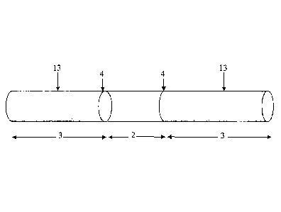
Fig. 5a shows schematically a conventional rod form element 1 comprising a hot
zone
2 and cold ends 3 meeting at hot zone/cold end interfaces 4 formed by the
junction
between the different materials of the hot zone and the cold ends.
A typical method of manufacture is to form the hot zone 2 and cold ends 3
separately
and then join or weld them together to form the heating element. However, this
does
not prevent other traditional methods known in the art being used including
forming a
one piece body such as helical cut tubes. In the present invention, no special
treatment
is necessarily applied to the hot zone since it is desired to maintain the hot
zone at a
io relatively high resistance. However known processes such as forming a glaze
to the
element are not precluded. Any means known in the art to produce the hot zone
using
a silicon carbide base material is applicable. A suitable material is re-
crystallised
silicon carbide. The term `re-crystallised' indicates that after formation the
material is
heated to high temperatures (typically greater than 2400 C e.g. 2500 C) to
form a
self bonded structure comprising predominantly a-silicon carbide. Typical
resistivity
values of the hot zone range from 0.07S2.cm to 0.085 .cm.
Fig 1. shows an outline of a typical process used to manufacture a three piece
welded
heating element. For manufacturing the cold ends, predetermined amounts of
silicon
carbide powder of various particle size and purity and carbon and/or a carbon
source
(for example wood flour, rice hulls, wheat flour, walnut shell flour or any
other
appropriate source of carbon) are blended with a binder (for example a
cellulose based
binder) in a suitable mixer (for example a Hobart mixerTM) to the desired
rheology for
extrusion.
A typical formulation of the mix used for the cold end material is shown in
Table 2.
11
CA 02727111 2010-12-06
WO 2009/147436 PCT/GB2009/050618
Table 2
Material Commercial Name Quantity (wt%)
Black Silicon Carbide 36/70 Sika PCK 15.79
Green Silicon Carbide F80 Sika III 26.43
Carbon source/porosity inducer Wheat flour 17.21
Carbon source/porosity inducer Wood flour 6.71
Carbon source Petroleum coke powder 31.46
Binder Magnafloc 139 2.37
Wheat flour and wood flour provide a carbon source and introduce porosity in
the
material. 36/70 Sika and F80 Sika are commercially available silicon carbide
materials (supplied by Saint Gobain although other commercial equivalent
grades can
be used) and comprise predominantly a-silicon carbide. 36/70 Sika is black
silicon
carbide containing traces of minor impurities. F80 Sika is green silicon
carbide and
contains less impurities than black silicon carbide. Magnafloc is a
commercially
available anionic acrylamide copolymer based binder material, manufactured by
io CIBA (WT), Bradford. The formulation is not restricted to this recipe and
other
recipes comprising silicon carbide, other sources of carbon and binders known
in the
art can be used. However, for the purposes of explaining the present approach
the
recipe shown in Table 2 was used throughout all of the investigations.
is The mix is extruded into the desired shape although other forming
techniques (e.g.
pressing or rolling) may be used if appropriate. Conventional heating element
shapes
include rods or tubes. Once extruded, the shaped mix is allowed to dry to
remove
moisture and then calcined to carbonise the wheatflour and the wood flour
carbon
precursors so as to introduce porosity into the bulk material. Typically the
porosity is
20 above 40% resulting in a bulk density in the range 1.3 to 1.5 g.cm 3. The
calcined
material is then cut to the desired shape. For the jointed elements, a spigot
manufactured from calcined cold end material may attached to one end by means
of a
cement comprising of a mixture of resin, silicon carbide and carbon. The
spigot
prepares the cold end material for attachment onto the hot zone material. (It
is not
12
CA 02727111 2010-12-06
WO 2009/147436 PCT/GB2009/050618
necessary to use a spigot - welds can be made without a spigot - however a
spigot
reinforces the mechanical strength of the joint).
The final stage of preparation of the cold end is siliconising. This comprises
the
reaction of silicon with the carbon present and infiltration of molten silicon
into the
porosity of the calcined material. The calcined bar together with the attached
spigot is
placed in a boat and covered with a mixture of a controlled amount of silicon
metal,
vegetable oil and graphite powder, typically in in the ratio 100:3:4. The
amount of
silicon required depends upon the porosity of the calcined bar - the lower the
porosity
io the less silicon is required. Typical amounts are 1.4-2 (for example 1.6)
times the
weight of the calcined bar.
Typically a graphite boat is used for the siliconising step. The purity of the
silicon
metal is important so as to prevent any impurities interfering with the
siliconising
is step. Various commercial silicon metals may be used depending upon grain
size and
purity. Typical impurities found in silicon metal are aluminium, calcium, and
iron.
The boat containing the calcined bar and silicon/carbon mixture is then heated
in a
furnace under a protective atmosphere (for example flowing nitrogen) to a
20 temperature in excess of 2150 C. A protective atmosphere limits undesirable
oxidation of furnace components as well as the calcined material and silicon
mixture
at the high temperature. A nitrogen containing atmosphere is desirable as
nitrogen acts
a dopant of the silicon carbide formed. At this temperature, the silicon metal
melts
and infiltrates the pore structure of the calcined material whereby some
reacts with the
25 carbon in the body to form secondary silicon carbide and the remaining
silicon fills
the pore structure to provide an almost fully dense silicon-silicon carbide
composite.
During the siliconising process, the silicon metal also permeates the joint
between the
spigot and the bulk material and reacts with excess carbon in the cement
material to
30 form a high temperature reaction bonded joint with the spigot.
The hot zone is made by analogous mixing, forming (e.g. by extrusion), and
drying
steps but not necessarily from the same mixture as the cold end [porosity for
13
CA 02727111 2010-12-06
WO 2009/147436 PCT/GB2009/050618
siliconising is not required for the hot zone] and is then recrystallised. For
the
purposes of this approach any hot zone material of appropriate resistance may
be used
and appropriate recrystallised a-silicon carbide bodies are available
commercially.
The hot zone may then be attached to the cold end [i.e. to the other end of
the spigot]
using the same cement material completing the heating element. The heating
element
including the attached hot portion is then re-fired to temperatures sufficient
to reaction
bond the hot zone to the spigot. A typical temperature is between 1900 C and
2000 C
which is below the temperatures at which (3-SiC transforms to a-SiC.
Optionally, a
glaze or coating can be applied to the heating element to provide chemical
protection
to the under body..
As indicated above, other methods may be used for securing the hot zone to the
cold
ends without the use of a spigot.
If required a glaze may be applied to the element.
Conventionally, the surface of the cold end near the terminal end is then
prepared to
provide a smooth surface such as by sand blasting for a metallisation step. A
metallisation coating provides an area of low electrical resistance so as to
protect any
attached electrical contacts from overheating. A metallisation layer such as
aluminium
metal is applied to the surface of a proportion of the cold end at the
terminal ends by
spraying or other means known in the art. Contact straps are then fitted over
the
metallised area to provide sufficient electrical connectivity to a power
source. Further
detail of the metallisation step is discussed below.
The present applicant has realised that by controlling the reaction parameters
during
the siliconising stage conditions can be created to promote (3-silicon carbide
formation
rather than a-silicon carbide. The reaction rate is controlled by controlling
process
parameters such as silicon particle size, impurities and the reaction time
during the
siliconisation stage. By inhibiting the formation of a-silicon carbide at the
siliconising
temperature and increasing the proportion of (3-silicon carbide in the bulk
material of
the cold end, the resistivity is reduced, resulting in an improved resistance
ratio of the
14
CA 02727111 2010-12-06
WO 2009/147436 PCT/GB2009/050618
element. A number of process changes were used by the present applicant, each
contributing to reducing the electrical resistance of the cold end bulk
material. By
combining these effects, the overall electrical resistance of the cold end may
be
substantially reduced. Below shows the process parameters investigated by the
present
applicant to reduce the electrical resistance of the cold end material.
Various commercial silicon metals having varying degrees of aluminium impurity
were used in the manufacture of cold end materials. Table 3 shows the various
commercial silicon metals used.
Table 3
Supplier Grain Size specified (mm) Aluminium Content (%)
Elkem 0.5 -3 0.04
Elkem 0.2 - 2 0.17
Graystar LLC 0.5-6.0 0.21
S & A Blackwell 0.5-3.0 0.25
Variation in resistivity with aluminium content was found but it was evident
that
particle size of the silicon metal had a greater effect. The samples made
using the
Graystar LLC sourced material, having an aluminium content of 0.21% and a
particle
size in the range of 0.5-6.0 mm showed the least resistivity and so this
aluminium
1s content was used in all subsequent tests.
In order to isolate the effects of grain size on the resistivity of the cold
end material
from the other parameters, trials were performed using silicon metals during
the
siliconising procedure having a constant aluminium content of 0.21%
(established in
the earlier investigation) but varying grain size (see Table 4). Fig 3 shows
the
variation of electrical resistivity with temperature for cold ends produced
using silicon
with varying grain sizes. All samples were processed in a graphite tube
furnace at
constant temperature of 2180 C and constant furnace push rate of -2.54
cm/minute
(1"/minute). The graph shows that there is a relationship between the particle
size of
the silicon with the resistivity of the cold end material. A particle size of
less than
0.5mm was considered detrimental to the process, although as discussed below
lower
particle sizes can be tolerated with suitable changes to manufacturing
conditions.
CA 02727111 2010-12-06
WO 2009/147436 PCT/GB2009/050618
Table 4
Supplier Grain Size Specified (mm) Aluminium Content (%)
S & A Blackwell 0.5-6.0 0.21
S & A Blackwell 0.25-6.0 0.21
S & A Blackwell 0.5-3.0 0.21
S & A Blackwell 0.2-2.0 0.21
Increasing the silicon particle size tends to reduce the rate of reaction of
silicon and
carbon such that the conditions for the formation of a-silicon carbide are not
favourable. Consequently, (3-silicon carbide is preferentially formed. Of
course, too
large a silicon particle size will result in poor coverage of the article
being siliconised
and may lead to inhomogeneity in the element produced. A minimum particle size
of
0.5mm is preferred, although as can be seen from Fig. 2, lower values can be
tolerated.
Other controlling parameters affecting the reaction parameters and thereby
affecting
the resistivity of the cold end, are the reaction temperature, the ramp rate
to
temperature, and the dwell time at the reaction temperature.
(3-silicon carbide starts to convert to a-silicon carbide only at about 2100
C, and
therefore, one would presume that by reducing the reaction temperature more 0-
silicon carbide would preferentially be formed. Siliconising the cold end
material at
temperatures ranging from 1900 C to 2180 C conducted in a tunnel furnace at a
push
rate of -4.57 cm/minute (1.8 inch/min) and -2.54 cm/minute (1 inch/min)
revealed no
clear relationship between the resistivity of the cold end material and the
furnace
temperature. In the majority of cases, the minimum resistivity value achieved
was at a
maximum furnace temperature of 2180 C, although for the reasons expressed
below
this need not be the maximum temperature experienced by the product. At
relatively
low temperatures such as 1900 C siliconising was found to be incomplete and in
areas
the material remained unreacted.
16
CA 02727111 2010-12-06
WO 2009/147436 PCT/GB2009/050618
In order to enable the reaction of silicon and carbon, a temperature in excess
of
2150 C appears to be advisable. This appears to be due to the fact that at
atmospheric
pressure, silicon oxide will not vapourise at lower temperatures and acts as a
barrier to
silicon movement. Any reaction between silicon oxide and carbon will also only
occur
at such temperatures.. It has been shown that siliconising under a vacuum
allows the
reaction to occur at much lower temperatures, for example 1700 C because
vapourisation of silicon oxide occurs at lower temperatures in a vacuum. The
applicant however believes that nitrogen is necessary as a dopant in order to
optimise
the resistivity of the cold ends rendering processing in a vacuum impractical.
A
partial pressure of nitrogen has been shown to decrease the resistivity of the
product.
However, at temperatures above 2150 C a-silicon carbide is formed.
Once the reaction is underway, the reaction between silicon metal and carbon
is,
1s exothermic. The exotherm results in a localised temperature increase within
the
carrier boats holding the carbonaceous silicon carbide and silicon. As a-
silicon
carbide is stable at higher temperatures than (3-silicon carbide, the
applicant believes
that the localised temperature increase results in a-silicon carbide being
formed in
preference to (3-silicon carbide. By controlling the effects of the exotherm,
the
transformation of (3-silicon carbide to a-silicon carbide can be inhibited to
some
extent.
The effect of the exotherm can be controlled by the ramp rate to temperature,
for
example, in a tube furnace, by controlling the push rate through the furnace.
Fig. 6a
shows conceptually as a temperature/time diagram what is happening during a
typical
siliconisation step in a graphite tube furnace having a temperature profile
with a
uniform ramp rate to maximum temperature, a plateau at temperature, and a
uniform
cooling rate. As a carrier boat containing articles for siliconising passes
through the
furnace it experiences a furnace environment having the profile of the solid
line
represented by a ramp rate to temperature 5, a plateau temperature 6, and a
cooling
rate 7 down from temperature. The temperature of an article carried by the
boat
follows the temperature profile of the furnace until silicon begins to react
with carbon.
The exothermic nature of this reaction means that the article will experience
a
17
CA 02727111 2010-12-06
WO 2009/147436 PCT/GB2009/050618
localised temperature above that in the furnace environment. This is shown by
the
dotted line 8, indicating maximum temperature 9, with the temperature increase
attributable to the exotherm being indicated as arrow 10.
s Fig. 6b shows the temperature for the same tube furnace but with a lower
push rate of
the carrier boat through the furnace. Although the rate of temperature
increase of the
article is slower during the initial heating cycle, this only becomes critical
when the
silicon oxide begins to vapourise. During this period, controlled evolution of
silicon
oxide vapour acts as a restriction on rapid infiltration of silicon into the
article. This
io effectively controls the exothermic reaction of carbon and silicon,
limiting the
localised temperature increase. Additionally the slower rise to temperature
gives a
longer time for the heat generated by the exotherm to escape, so limiting the
localised
temperature increase. These limitations to the localised temperature increase
result in
a reduced conversion of (3-silicon carbide to a-silicon carbide so resulting
in a higher
15 (3-silicon carbide to a-silicon carbide ratio in the fired material.
It will be noted that another result of slowing the push rate is that the ramp
down from
temperature takes longer and the time at the plateau is longer. This may
facilitate
more complete siliconising of the article and so increase the yield of (3-
silicon carbide.
20 Of course too long at maximum temperature (if above 2100 C) may start to
result in
transformation of (3-silicon carbide to a-silicon carbide and so the actual
time and
temperature profile to use may vary. These times can be changed by using a
tube
furnace having a different temperature profile as indicated schematically in
Fig. 6c in
which a slow ramp up rate 5 as in Fig. 6b is combined with a faster ramp down
rate 7
25 as in Fig. 6a.
In the above reference has been made to a tube furnace. It will be evident
that similar
temperature profiles may be obtained in other furnaces operating in batch or
continuous mode with appropriate control of temperature and atmosphere.
Further,
30 more complex profiles can be adopted [e.g. a ramp rate to a first
temperature, a dwell
at that temperature to permit a large fraction of siliconising to occur, and
then a
change to a second temperature to permit the balance of siliconising to
occur].
18
CA 02727111 2010-12-06
WO 2009/147436 PCT/GB2009/050618
In order to investigate the effects of reaction time, a graphite tube furnace
was used.
The furnace used had internal dimensions -20.3cm (8") diameter x -152.4cm
(60")
long. By varying the push rate through the furnace, the duration at the
reaction
temperature can be varied thereby controlling the reaction rate. The faster
the push
rate, the shorter the reaction time and conversely the slower the push rate
the longer
the reaction time. However, this does not prevent other furnaces known in the
art
being used that can provide varying reaction temperatures and reaction times.
Taking these factors into consideration, the present applicant investigated
the
io resistivity of the cold end material siliconised at various push rates
ranging from
-1.27cm/min (0.5 in/min) to -4.57cm/min (1.8 in/min) at a fixed furnace
temperature
of 2180 C. In these investigations Graystar silicon metal (as indicated in
Table 3
above) was used, a minimum resistivity was obtained for a push rate of -
1.27cm/min
(0.5 in/min). Fig. 3 shows a plot of resistivity of the cold end material
versus
is temperature when siliconised at different push rates. The reduction in
resistivity
achieved by slowing the push rate from -2.54cm/min (1 in/min) to -1.27cm/min
(0.5
in/min) is small compared with that when the push rate is reduced from -3.81
cm/min
(1.5 in/min) to -2.54cm/min (1 in/min). Although the push rate of -1.27cm/min
(0.5
in/min) showed the greatest reduction in resistivity, such a slow push rate
may limit
20 production capacity. A compromise can thus be made between the duration at
the
reaction temperature and production requirements. With the particular furnace
used, a
push rate of -2.54 cm/minute (1 inch/minute) was considered optimum.
Example 1
25 This example aimed to make elements of similar geometry to the commenrcial
element type Globar SD being 20 mm diameter, with a 250 mm hot zone length,
and a
450 mm cold end length, and resistance 1.44 ohms
A cold end mix was made according to the recipe shown in Table 2 (Mix A) and
30 extruded into a tube. After calcining, the rod was cut into approximately
450mm
lengths and a spigot attached to the cold end material by applying a cement
comprising silicon carbide, resin and carbon. The tube together with the
spigot was
then placed in a graphite boat for the siliconising stage and covered in a
blanket of a
19
CA 02727111 2010-12-06
WO 2009/147436 PCT/GB2009/050618
predetermined amount of silicon metal and carbon. The cold end material was
then
siliconised using the process steps described above. These are:-
The particle size distribution of silicon was 0. 5 - 6.0mm;
The furnace push rate set to -2.54cm/min (1 inch/min);
The aluminium content of the silicon was 0.21 %.
The cold end material was siliconised at a temperature of 2180 C. After the
siliconising stage, a hot zone was attached onto the spigot of the cold end
using the
cement. A cold end was attached to either end of the hot zone. The hot zone
was a
250mm long recrystallised Globar SD Hot Zone material commercially available
from
Kanthal and identified as Mix B. The combination of the cold ends and the hot
zone
was then fired in a furnace to a temperature between 1900 C and 2000 C, to
reaction
bond the hot zone to the spigotted cold ends.
By using the optimised process parameters discussed above, resistivity of the
cold end
decreased from 0.03 S cm for a conventional cold end to 0.012 S cm at 600 C,
which
according to Ohm's Law represents a decrease in dissipated power of 66%. In
terms
of ratio of resistance of hot zone per unit length to cold end per unit
length, the above
techniques results in a ratio of 60:1 compared with 30:1 for commercial
available
standard material.
To measure the energy efficiency that results from the present approach, a
formed
heating element was installed into a simple brick lined furnace and the power
required
to maintain a furnace temperature of 1250 C was measured and compared against
a
standard Globar element commercially available from Kanthal of exactly the
same
dimensions and resistance, the only difference being the cold end resistivity
as
described above.
The power consumed from the standard heating element was 1286W but using the
material according to the present approach a power of only 1160W was consumed,
which represents a power saving of 126W or 9.8%.
CA 02727111 2010-12-06
WO 2009/147436 PCT/GB2009/050618
Example 2
As a further illustration of the advantages of the present approach,
comparisons were
made between samples prepared using the technique described in Example 1 with
known samples currently on the market. Samples were randomly taken from each
of
the cold ends and hot zone from a number of heating elements. Samples 1 to 2
represent material that have undergone different process treatments and
Samples 3
and 4 represent commercial materials. A description of each sample type is
shown in
Table 5.
Table 5
Sample Type Description
Sample 1 Material according to the present approach
(Graystar silicon 0.25-6.0mm; 0.20% Al; furnace
push rate 1 inch/min) - see Example 1
Sample 2 (Comparative) Sample 1 but furnace push rate set to 1.8 inch/min
Sample 3 (Comparative) Commercial material (Erema E )
Sample 4 (Comparative) Commercial material (12R Type )
io Due to the difficulty in accurately differentiating between a-silicon
carbide and f3-
silicon carbide using x-ray diffraction techniques, samples were analysed
using
Electron Back Scattered Diffraction (EBSD). As is known in the art, EBSD uses
back
scattered electrons emitted from the sample in a SEM to form a diffraction
pattern that
is imaged on a phosphor screen. Analysis of the diffraction pattern allows the
is identification of the phases present and their crystal orientation.
Backscattered and
fore-scatter detector (FSD) image were gathered using the diodes on a NordlysS
detector. Secondary and in-lens images were gathered using the detectors on
the SEM.
The EBSD patterns were gathered and saved using the OI-HKL NordlysS detector.
The EBSD and Energy Dispersive Analysis Spectrum (EDS) maps were gathered
20 using 01-HKL CHANNELS software (INCA-Synergy). By setting the EBSD to
analyse the diffraction pattern generated by the phases:
= a-silicon carbide (SiC 6H);
= (3-silicon carbide (SiC 3C);
= silicon;
21
CA 02727111 2010-12-06
WO 2009/147436 PCT/GB2009/050618
and
= carbon
their quantitative amounts can thus be determined. The crystal structures of
the phases
used in the analysis is shown in Table 6.
Table 6
Phase Crystal Structure Lattice parameter (A)
SiC 3C (0) Cubic a = 4.36
SiC 6H (a) Hexagonal a = 3.08, c = 15.12
Si Cubic a = 5.43
C Amorphous -
Figure 4a shows a backscattered image for Sample 1. The different contrasts in
the
image represent the different phases in the body of the material. The dark
areas
represent graphite, the grey areas represent silicon carbide and the light
areas
represent silicon. The phase contrast between a-silicon carbide phase (SiC 6H)
and f3-
silicon carbide phase (SiC 3C) can be made out in the SEM in-lens detector
image
shown in Fig. 4b. The grey areas represent the (3-silicon carbide phase (SiC
3C) and
the lighter areas represent the a-silicon carbide phase (SiC 6H). The
remainder of the
body is a matrix of carbon and silicon. Image analysis was used to measure the
1s proportion of a-silicon carbide phase (SiC 6H) and (3-silicon carbide phase
(SiC 3C)
in the image.
Table 7 shows a breakdown of the results for Samples 1 to 4 measured using the
above technique and comparisons were made with their corresponding electrical
properties.
22
CA 02727111 2010-12-06
WO 2009/147436 PCT/GB2009/050618
Table 7
Properties Sample 1 Sample 2 Sample 3 Sample 4
SiC 3C (0) Vol% 51 37 36 31
SiC 6H (a) Vol% 28 30 36 14
Silicon Vol% 15 15 15 7
Carbon Vol% 6 18 13 48
Mean Resistivity of Cold End S2.cm 0.001269 0.002473 0.003600 0.002368
Mean Resistance per unit length of 0.000550 0.001071 0.001522 0.001099
Cold End (RCE) 52 /cm
Mean Resistivity of Hot Zone S2.cm 0.070184 0.073076 0.075119 0.071737
Mean Resistance per unit length of Hot 0.030394 0.031646 0.031765 0.033296
Zone (RHE) S2/cm
Mean Ratio of RHE:RCE (equivalent 55.300 29.5474 20.8636 30.29327
to ratio of resistivity as uniform cross
section)
Sample 1 represents the optimum material formulated according to an embodiment
of
the present approach and demonstrates a positive relationship between the
proportion
of (3-silicon carbide (51vol%) in the body with its corresponding electrical
properties.
Moreover, Sample 1 yields the greatest proportion of total SiC (51vol% +
28vo1%).
By optimally controlling the process parameters, more SiC is generated through
reaction alone.
Comparing Sample 1 with Samples 2 and 3 it can be seen that the increased
proportion of (3-silicon carbide in Sample 1 (51% compared with 37% and 36% in
Samples 2 and 3) results in a lower resistivity material . The effect of the
reduced
resistivity has a direct effect in improving the ratio of the resistance per
unit length of
the hot zone to cold end.
23
CA 02727111 2010-12-06
WO 2009/147436 PCT/GB2009/050618
Thus, by optimising the control parameters during the reaction between silicon
and
carbon, conditions that promote the formation of the more electrically
conductive f3-
silicon carbide (SiC 3C) component can be created.
Traditionally only a small area of the cold end body at the terminal ends is
metallised
in order to create an area of lowered contact resistance onto which metallic
contact
straps such as aluminium braid are fitted with spring clips or clamps. This is
to
prevent the electrical contacts from overheating and thus, degrading. This has
been
the norm for many years. For example, Table 8 below indicates the diameter,
cold end
length and metallised length for some commercial elements from two
manufacturers.
Also shown are the % of cold end sprayed and the ratio of the metallised
length to
diameter. Typically, aluminium metal is used for the metallisation process
Table 8
Diameter Min cold end Metallised % cold end Metallised
(mm) length (mm) length (mm) sprayed length/diamete
Kanthal
10 100 50 50.0% 5.00
12 100 50 50.0% 4.17
14 100 50 50.0% 3.57
16 100 50 50.0% 3.13
100 50 50.0% 2.50
200 50 25.0% 2.00
32 250 70 28.0% 2.19
38 250 70 28.0% 1.84
45 250 70 28.0% 1.56
55 250 70 28.0% 1.27
Erema
10 150 30 20.0% 3.00
12 150 30 20.0% 2.50
14 200 30 15.0% 2.14
16 250 30 12.0% 1.88
20 300 50 16.7% 2.50
25 300 50 16.7% 2.00
300 50 16.7% 1.67
300 50 16.7% 1.43
300 50 16.7% 1.25
400 50 12.5% 1.11
400 50 12.5% 1.00
24
CA 02727111 2010-12-06
WO 2009/147436 PCT/GB2009/050618
The present applicant has realised that by applying an electrically conductive
coating
along an increased proportion of the length, a reduced resistance path is
provided to
the hot zone, thereby increasing the electrical resistance ratio of the hot
zone to the
cold end. This is demonstrated by a schematic representation of the heating
element as
shown in Fig 5(a and b). Fig. 5a shows the case using traditional
metallisation
techniques in which terminal portions 12 are provided to permit contact with
conductors. The cold ends between terminal portions 12 and the cold end//hot
zone
interfaces 4 are not metallised. Over this non-metallised portion current
transfer is
entirely through the material of the cold end.
By applying a conductive coating over 70% or more of the length of the cold
end
[>70%, or >80% or >90%, or even the entire cold end] an additional path for
current
is provided in parallel with the cold end material. This conductive coating
may be a
metallisation. Fig. 5b shows an element in accordance with this aspect in
which a
1s conductive coating (12, 13) extends over a large part of the surface of the
cold end
providing both a parallel and preferred conductive path 13, and, at the ends
remote
from the hot zone, terminal portions 12.
Although aluminium has traditionally been used, and could be used in the
present
invention, in some cases it is not best suited as a coating material because
the high
temperatures experienced near the hot zone may tend to degrade the aluminium
coating. Metals more resistant to degradation at high temperatures may be
used.
Typically such metals would have melting points above 1200 C, or even above
1400 C. Example of such metals include iron, chromium, nickel or a combination
thereof, but the invention is not limited to these metals. In the most
demanding
applications more refractory metals could be used if desired. Although metals
have
been mentioned above any mechanically and thermally acceptable material that
has a
significantly lower electrical resistivity than the material of the cold end
would
achieve a benefit over an untreated cold end.
Moreover, more than one type of coating can be applied to the cold end to
cater for
the different temperatures experienced along the cold end. For example,
aluminium
metal could be used near the terminal end or electrical contact area where it
is
CA 02727111 2010-12-06
WO 2009/147436 PCT/GB2009/050618
relatively cold and a higher melting point metal, or one less reactive, could
be used at
the higher temperature region near the hot zone.
Since the metallisation process provides an area of lowered resistance, it has
the
advantage that it can improve existing high resistive materials and that is
the subject
of the presently claimed invention. For example, the metallisation coating can
be used
to convert a high resistive recrystallised body which would generally be used
for the
hot zone, to a cold end and yet be able to provide a respectable electrical
resistance
ratio, for example in the order of 30:1.
In some cases, this does away with the need to formulate a separate cold end
body and
would also enable elements of one piece construction to be utilised. In some
applications one piece elements have advantages in terms of mechanical
strength.
Fig.8 shows an element formed of a single piece of recrystallised silicon
carbide in
which the extent of metallisation 13 defines the cold ends 3.
Furthermore, cold ends of multiple sections can be manufactured. Such cold
ends
would have the advantage that the thermal conductivity of the recrystallised
material
is believed to be below the thermal conductivity of the normal cold end
material and
so acts to reduce heat loss through the cold end. Such an element is shown in
Fig. 7a)
described below.
In other instances, the conductive coating would equally be applicable to
heating
elements formed as one piece such as helical tubular rods. Typical rods of
this type
are CrusiliteTM Type X elements and GlobarTM SG and SR rods. When applied to
the
cold end formed by the first approach described above, the effect of the
metallisation
coating increases the electrical resistance per unit length ratio to values
exceeding
100:1.
Traditionally, the coating is applied by flame spraying aluminium wire.so that
the
aluminium adheres to the surface of the body. The present applicant has
realised that
the coating process is not restricted to such techniques and other coating
techniques
can be used, and for some metals will necessarily be used. Examples of such
methods
26
CA 02727111 2010-12-06
WO 2009/147436 PCT/GB2009/050618
include plasma spraying and arc spraying. Arc spraying can be used for some
high
temperature resistant metals, for example Kanthal spray wire - a range of
FeCrAl
FeCrAlY and Ni-Al alloys - and these materials can conveniently be used in the
present invention.
Example 3
To verify the effects of a metal coating independent of the underlying body,
the
metallisation technique of the present invention was applied to two types of
cold end
body materials.
The first element (Fig. 5b) was as described in Example 1.
The second element (Fig. 7a) was of like dimensions to the first element, but
comprised a hot zone 14 with hybrid cold ends 15 comprising one part 16 formed
1s from the mixture of Table 2 siliconised according to the process parameters
described
in Example 1, and a second part 17 formed from recrystallised hot zone
material (Mix
B).
In both cases the length of the cold end was kept to 450mm. For the hybrid
material,
100mm of its length is formed from Mix A and the remaining part of the cold
end is
extended to 450mm by attaching 350mm of recrystallised hot zone material (Mix
B).
The hot zone body made from Mix B consisting of recrystallised Globar SD (see
Table 2) was then attached to the cold end body material to complete the
heating
element. The cold end (450mm) was then metallised by spraying with aluminium
metal. In the particular investigation the entire length of the cold end was
metallised
but it will be evident that this is not a necessary requirment.
The heating element was then installed into a simple brick-lined furnace and
the
power required for maintaining the furnace temperature at 1250 C was measured.
Comparisons were made with a standard "GLOBAR SD" heating element of like hot
zone and cold end dimensions to the first and second element, but metalllised
as
known in the art, i.e. where only 50mm of the cold end is metallised (see Fig.
5a).
27
CA 02727111 2010-12-06
WO 2009/147436 PCT/GB2009/050618
It was found that the power consumed from the standard heating element (Fig.
5a)
was 1286W but using the improved metallisation step according to the present
invention, a power consumption of only 1160W was consumed when the cold end
s body was made entirely of Mix A (Fig. 5b), which represents a power saving
of 126W
or 9.8%. Moreover, using the improved metallisation process on the hybrid cold
end
material consisting partially of recrystallised hot zone material (Fig. 7a), a
power of
1203W was consumed, representing a power saving of 83W or 6.4%.
io Although the underlying hybrid cold end body of fig 7a is not as efficient
as the cold
end described in Example 1 [Fig. 5b], the lower power consumption in
comparison to
standard heating elements known in the art demonstrates the benefits of
overspraying
the cold end body thereby creating an area of reduced resistance.
15 Example 4
In a further test, comparisons were made to see the effects of metallising an
underlying cold end body using the improved metallisation step according to
the
present invention. In these tests 200mm (80% of the cold end length) from the
terminal end was metallised compared to 50 mm (20% of the cold end length) as
in
20 known art. In both cases, the metallising coating was applied to a cold end
formed
using the process parameters as described in Example 1.
The heating element was made to the following size:-
Hot Zone:- 950mm (recrystallised Globar SDTM)
25 Cold End:- 250mm
The power required to maintain the heating elements at a hot zone surface
temperature
of 1000 C in free air was measured. Using the conventional terminal
metallisation
technique, the ratio of the electrical resistance per unit length of the hot
zone to the
30 cold end was measured to be 54:1. However, using the metallisation coating
of the
present invention, the ratio improved to 103:1, which by calculation from
Ohm's Law
represents a substantial reduction in power dissipation of 50%.
28
CA 02727111 2010-12-06
WO 2009/147436 PCT/GB2009/050618
The reduced resistivity of the new cold end materials of the present invention
is
accompanied to some extent by an increase in thermal conductivity which can
offset
to a degree some of the advantages of the material. However, this can be put
to
advantage in that the cross-section of the cold end can be reduced while still
retaining
an acceptably good ratio of hot zone to cold end electrical resistivity (e.g.
30:1). Such
a construction reduces heat transfer within the cold end in comparison with a
full
diameter cold end of the same material. This reduction in cross section can be
achieved for tube elements by increasing the inner diameter of the cold end
tube while
leaving the outer diameter constant to match the outer diameter of the hot
zone.
However, it is preferable to instead reduce the outer diameter of the cold
ends so that
they are narrower than the hot zone. This has particular advantage in that:-
the radiating surface of the cold end is reduced, so reducing heat loss
= the cold ends can be covered with thermally insulating material or a
thermally
insulating sleeve to reduce heat loss still further
= the insulating material or insulating sleeve need not extend beyond the
outer
diameter of the hot zone.
Heat transfer through the cold ends can also be reduced by thinning or
perforating the
material at selected points in the cold ends (e.g. by use of slots), and this
can be
combined with reducing the thickness of the material over all or part of the
cold ends
Providing thermally insulated cold ends will result in reduced heat loss and
so a raised
temperature of the cold end. This elevation in temperature will result in a
lowering of
resistivity and hence of cold end resistance.
The cold end does not to be reduced in cross-section over its entire length.
Example 5
Elements as specified in Table 9 below were tested in a specially-built
Element Test
Furnace, constructed by Carbolite, furnace design number 3-03-414 in such a
way that
all external ambient conditions had no effect on the power required to hold
the
furnace at temperature. Using this furnace, it was possible to control and
monitor all
aspects of the conditions in which the elements were tested including:-
furnace temperature;
29
CA 02727111 2010-12-06
WO 2009/147436 PCT/GB2009/050618
= desired surface power load applied to the elements (by use of water-cooled
tubes acting as an artificial load extracting heat from the furnace); and,
= the atmospheric conditions.
The elements were tested in sets of three at a time, the power to each element
being
separately controlled depending on the resistance of each element. Each test
was
conducted under a constant flow of dry nitrogen gas regulated into the furnace
at 20
litres/min. This gave constant atmospheric conditions. The furnace insulation,
element lead-in holes, aluminium straps and element power clip connections
remained
constant throughout testing of the various element types. The power applied to
each
element was monitored at 10 minute intervals and in this way a determination
of the
point at which equilibrium or steady state conditions applied (power supplied
matching heat loss to the load and environment) could be made.
Table 9
Cold
End
Resistance Cross Mean
ratio section Power Saving
Element Type RHE:RCE (cm) (W) (%)
3 piece element as Fig. 5a, conventional
material cold ends - Cold end material as
Sample 2, Table 5
Cold end 19.1 mm outer diameter (OD) x
8.5 mm inner diameter (ID) 25.0 2.3 8537.36
3 piece element as Fig. 5a , low resistivity
cold ends
Cold end material as Sample 1, Table 5
Cold end 19.1 mm OD x 8.5 mm ID 65.2 2.3 8369.68 1.97
3 piece element with insulated 14 mm
cold ends as Fig. 7b
Cold end material as Sample 2, Table 5
Cold End 14.0 mm x 7.5 mm ID
Hot zone l9.lmm OD 27.2 1.1 8331.45 2.41
3 piece Globar SD with 14 mm insulated
and plugged cold ends as Fig.7b, with
bore insulated
Cold end material as Sample 2, Table 5
Cold End 14.0 mm x 7.5 mm ID
Hot zone l9.lmm OD 27.2 1.1 8318.78 2.56
1s Under these test conditions results as detailed in Table 9 were obtained
for elements
[of Globar SD 20-600-1300-2.30 design within modifications indicated in Table
9],
CA 02727111 2010-12-06
WO 2009/147436 PCT/GB2009/050618
where the diameter is nominally 20 mm and the hot zone length is 600 mm and
the
overall length is 1300 mm and the nominal resistance is 2.30 ohms. The furnace
temperature was set at 1000 C and the water cooling system arranged in such a
way
that a surface power loading on the elements of approximately 8.5 Watts/cm was
achieved. These conditions are representative of one set of typical conditions
under
which such elements can be used.
As can be seen, the change from standard cold end material with geometry as
defined
in Fig 5a to new cold end material yields a 1.97% reduction in power use at
equilibrium.
In reducing the cross sectional area of the cold end and applying a 2.5 mm
thick layer
of ceramic fibre insulation material 18 as shown in Fig. 7c, in this case to
47.8% of
the original, the element ratio decreases from 65: 1 to 27 : 1 but the power
saving is
seen to improve from 1.97% to 2.41%. This clearly demonstrates that despite a
decreased hot zone:cold end resistance ratio, the efficiency of the heating
element is
improved as a result of the reduction of the cross section. Insulating the
cold ends has
the combined effect of preventing heat loss and increasing the material
temperature,
thereby further reducing the resistivity. Also the nominal diameter of the
element
remains unchanged and the element continues to be easily located into a lead-
in hole
in a furnace with no additional insulation or plugging required.
Furthermore, if the cold ends are insulated with a 2.5 mm thick ceramic fibre
insulating material, a further power reduction is realised from 1.97% to 2.56%
over
standard. Insulating the bore of the cold ends has an additional effect of
preventing
heat loss and increasing the cold end material temperature, thereby further
reducing
the resistivity
Example 6.
To provide a comparable set of performance results a number of elements
tubular
elements were made which [except where indicated] had nominal 20mm diameter
cold ends each of 375mm length bracketing a 20mm diameter hot zone of 600mm
length. Actual diameters were:-
31
CA 02727111 2010-12-06
WO 2009/147436 PCT/GB2009/050618
Nominal diameter Minimum outer Maximum outer Minimum inner Maximum inner
(mm) diameter (mm) diameter (mm) diameter (mm) diameter (mm)
20 18.80 19.30 7.90 8.70
These elements were tested in the manner of Example 5 above and the 12 hour
equilibrium powers required to maintain a temperature of 1000 C are summarised
in
Table 10.
Power % % Resistance
[W] Power Saving ratio
[A] A one piece recrystallised silicon 8410 100 0 13.1
carbide element in which end portions were
impregnated with silicon to form the cold
ends
[B] A one piece recrystallised silicon 8416 100.07 -0.07 13.2
carbide element in which end portions were
impregnated with silicon to form the cold
ends and the bore of the tube plugged with
refractory fibre
[C] A three piece recrystallised silicon 8424 100.17 -0.17 24.7
carbide hot zone having silicon
impregnated silicon carbide cold ends
bonded to the hot zone
[D] A three piece recrystallised silicon 8357 99.38 0.62 52.1
carbide hot zone having cold ends formed
by the first approach mentioned above
bonded to the hot zone
[E] A three piece recrystallised silicon 8375 99.59 0.41 25.3
carbide hot zone having 14 mm diameter
terminals cold ends formed by the first
approach mentioned above bonded to the
hot zone
[F] A single piece recrystallised silicon 8139 96.78 3.22 16.9
carbide element sprayed with metal
[FeCrAl] to form cold ends
[G] A single piece recrystallised silicon 8128 96.65 3.35 16.9
carbide element sprayed with metal
[FeCrAl] to form cold ends with the bore of
the tube plugged with refractory fibre
[H] A five piece element comprising a 8049 95.71 4.29 51
recrystallised silicon carbide hot zone,
75mm silicon impregnated cold end
portions attached to the hot zone, and
metallised recrystallised silicon carbide
terminal portions completing the cold zones
[Fig. 7a)
32
CA 02727111 2010-12-06
WO 2009/147436 PCT/GB2009/050618
As can be seen, in these tests, metallisation of a recrystallised silicon
carbide material
to form a cold end provided significant power savings over using conventional
silicon
impregnated cold ends. A hybrid element in which a material of lower
electrical
resistance than the recrystallised silicon carbide [e.g. silicon impregnated
silicon
carbide] is interposed between the recrystallised silicon carbide and the hot
zone
provided still better savings.
A further effect of using metallised recrystallised silicon carbide as a means
of
reducing heat loss from the ends of silicon carbide heating elements, is that
it results
in lower temperatures at the terminal end of the element. Fig. 9 shows the
results of
measurement of temperature in the bore of elements [A], [C], and [H] above. As
can
be seen the temperature at the terminal end [-25mm from the end] is
significantly
lower for element [H] in accordance with the present invention than for
elements [A]
and [C]. Lower terminal end temperatures will reduce the risk of overheating
of the
1s terminal straps.
The relative lengths of relatively low electrical resistance cold end material
and
metallised recrystallised silicon carbide can be chosen to meet the particular
application. The length of the section relatively low electrical resistance
cold end
material can be varied, according to the total length of the cold end, the
operating
temperature of the furnace, and the thickness and insulation properties of the
thermal
lining of the equipment. Preferably the relatively low electrical resistance
cold end
material will be less than 50% of the total length of the cold end that is
positioned
inside the thermal lining.
For example, if the thermal lining is 300mm thick, and the total cold end
length is
400mm, there will be 100mm length of cold end positioned outside the confines
of the
lining, to allow electrical connections to be made, and 300mm of cold end
within the
confines of the thermal lining. In this case, the preferred length of the
relatively low
electrical resistance cold end material interposed between the metallised
recrystallised
silicon carbide and the hot zone will be less than 50% of 300mm, or less than
150mm.
It will be apparent that more than just five sections [as in example [H]] can
be used in
constructing a silicon carbide heating element, and such constructions are
included in
the scope of the present invention.
33
CA 02727111 2010-12-06
WO 2009/147436 PCT/GB2009/050618
In the above, discussion has been primarily about tubular elements. It should
be
understood that the present invention encompasses rod elements and elements of
cross
section other than circular. Where the word "diameter" is used this should be
taken as
meaning the maximum diameter transverse to the longest axis of the element, or
part
of element, referred to.
The presently claimed invention only claims some of the inventive features
disclosed.
To preserve the right to file divisional application the applicant indicates
that one or
more of the following features alone or in combination may be the subject of
later
divisional applications.
i) A silicon carbide heating element having one or more hot zones and two or
more cold ends, the hot zones comprising a different silicon carbide
containing material from the cold ends, and in which the silicon carbide in
1s the material of the cold ends comprises sufficient (3-silicon carbide that
the
material has an electrical resistivity less than 0.002 Q.cm at 600 C and less
than 0.0015 Q.cm at 1000 C; optionally in which:-
= the material of the cold ends comprises a-silicon carbide and (3-silicon
carbide; optionally in which the volume fraction of (3-silicon carbide is
greater than the volume fraction of a-silicon carbide; and/or
= the ratio of the volume fraction of (3-silicon carbide to the volume
fraction
of a-silicon carbide is greater than 3:2; and/or
= the material of the cold ends comprises greater than 45vo1% (3-silicon
carbide; and/or
= the total amount of silicon carbide is greater than 70vol%; and/or
= the material of the cold end comprises:-
i. SiC 70-95vo1%
ii. Si 5-25vo1%
iii. C 0-l Ovol%
with SiC + Si + C making up >95% of the material of the material; and/or;
= the ratio of the electrical resistivity of the material of the hot zone to
the
electrical resistivity of the material of the cold end is greater than 40:1.
34
CA 02727111 2010-12-06
WO 2009/147436 PCT/GB2009/050618
ii) A method of manufacture of a cold end for a heating element, the method
comprising the step of exposing a carbonaceous silicon carbide body
comprising silicon carbide and carbon and/or carbon precursors, to silicon
at a controlled reaction temperature sufficient to enable the silicon to react
with the carbon and/or carbon produced from the carbon precursors to
form (3-silicon carbide in preference to a-silicon carbide, and for an
exposure time sufficient that the amount of (3-silicon carbide in the cold
end is sufficient that the material has an electrical resistivity less than
0.002 Q.cm at 600 C and less than 0.0015 Q.cm at 1000 C; optionally in
which:-
the reaction parameters are controlled to promote (3-silicon carbide
formation in preference to a-silicon carbide by controlling one or more of
the following process variables:-
b. silicon particle size
1s c. purity levels of the raw materials
d. ramp rate to reaction temperature; and/or.
= the silicon has a particle size greater than 0.5mm; and/or
= the silicon has a particle size in the range 0.5mm to 3mm.
iii) A silicon carbide heating element having one or more hot zones and two or
more cold ends, in which greater than 70% of the length of at least one
cold end is coated with a conductive coating having an electrical resistivity
lower than that of the material of the cold end; optionally in which:-.
= greater than 80% of the length of the cold end is coated with the
conductive coating; and/or
= greater than 90% of the length of the cold end is coated with the
conductive coating; and/or
= the ratio between the metallised length of the cold end to the maximum
dimension of the cold end transverse to the longest axis of the cold end is
greater than 7:1; and/or
= the conductive coating is metallic; and/or
= the conductive coating comprises aluminium; and/or
CA 02727111 2010-12-06
WO 2009/147436 PCT/GB2009/050618
= the metallic coating has a melting point above 1200 C; and/or
= the metallic coating has a melting point above 1400 C; and/or
= the metallic coating comprises nickel, chromium, iron, or mixtures thereof;
and/or
= the conductive coating changes in composition along its length, the
composition of the coating towards the hot zones having a greater stability
at high temperature than the composition of the coating remote from the
hot zones; and/or
= the coating is metallic comprising more than one metal type and in which
io the melting point of each metal type increases along the length of the cold
end from a first end for connection to an electrical source towards a second
end nearer the hot zones.
iv) A silicon carbide heating element as described above, in which the cross-
is sections of the cold ends at least for part of their length are less than
the
cross-sections of the hot zones optionally in which:-.
= the element is tubular; and/or
= the cold ends have a narrower wall thickness than the hot zones; and/or
= the outer diameter of the cold ends is less than the outer diameter of the
hot
20 zone; and/or.
= the cold ends are thinned or perforated at selected points; and/or
= the cold ends are thermally insulated; and/or
= the maximum dimension of the cold ends transverse to the longest axis of
the cold ends is less than the maximum dimension of the one or more hot
25 zones transverse to the longest axis of the one or more hot zones; and/or
36