Note: Descriptions are shown in the official language in which they were submitted.
CA 02727513 2011-01-06
BLANKET PROBE
FIELD
[0001] This relates to a blanket probe for non-destructive inspection of
metals such as
carbon steel, copper, brass, cupro-nickel, ferritic and other alloys with a
finite thickness.
BACKGROUND
[0002] RFT (remote field testing), which may also be referred to as RFEC
(remote field
eddy current) and RFET (remote field electromagnetic technique), can be used
to find defects
in carbon steel, copper, brass, cupro-nickel, ferritic and other alloys with a
finite thickness.
An example of a device that allows this is the Ferroscope 308, produced by
Russell NDE
Systems Inc. of Edmonton, Alberta, Canada (www.russelltech.com).
[0003] Using the Ferroscope 308, an RFT probe is moved down the inside of a
pipe or
tube and is able to detect inside and outside defects with approximately equal
sensitivity.
Although RFT works in nonferromagnetic materials such as copper and brass, its
sister
technology eddy current is also suitable for these materials.
[0004] The basic RFT probe consists of an exciter coil (also known as a
transmit or send
coil) which sends a signal to the detector (or receive coil). Exciter coil 20
is energized with an
AC current and emits an alternating electro-magnetic field. The field travels
outwards from
exciter coil 20, through the pipe wall, and along pipe 12. The detector is
placed inside pipe 12
two to three pipe diameters away from exciter 20 and detects the magnetic
field that has
travelled back in from the outside of the pipe wall (for a total of two
through-wall transits).
[0005] In areas of metal loss, the field arrives at the detector with a faster
travel time
(greater phase) and greater signal strength (amplitude) due to the reduced
path through the
steel. Hence the dominant mechanism of RFT is through-transmission, and the
dominant
energy source is the axial magnetic field.
SUMMARY
[0006] According to an aspect, there is provided a blanket probe for detecting
the
CA 02727513 2011-01-06
2
thickness of a wall having a non-planar surface. The blanket probe comprises a
probe portion
comprising a planar substrate that is flexible in one or two dimensions, an
array of detectors
mounted on the substrate and at least one interface for communicating signals
to and from
each detector.
[0007] According to other aspects, the substrate may be a flexible printed
circuit board.
The array of detectors may be a two dimensional array of detector coils. The
array of
detectors may be sensitive to an electromagnetic field having mutually
orthogonal directions.
The planar substrate may comprise one or more stiffeners to reduce flexibility
in one
dimension.
[0008] According to other aspects, the wall may be the wall of a pipe, tank or
vessel. The
wall may be made from at least one of carbon steel, copper, brass, cupro-
nickel, and ferritic.
[0009] According to another aspect, one or more multiplexers may connect the
array of
detectors to the at least one interface to serially record a detection signal.
[0010] According to other aspects, there may be at least one exciter for
exciting the wall.
The at least one exciter may generate an electromagnetic field. The blanket
probe may futher
comprise an operator unit for inputting instructions and displaying test
results, an interface
unit comprising the at least one interface for receiving detection signals
from the detectors
and sending control signals to the exciter unit, and an exciter unit for
controlling the at least
one exciter. The operator unit, the interface unit and the exciter unit may
communicate by
wired or wireless links. At least the operator unit and the interface unit may
be housed within
a portable housing.
[0011] According to other aspects, the wall may be a pipe wall and the at
least one exciter
is positioned on an opposite side of the pipe from the probe portion, inside
the pipe, or
adjacent to the probe portion.
[0012] According to another aspect, there is provided a method of testing a
non-planar
wall having a finite thickness, comprising the steps of: positioning a planar
substrate that is
CA 02727513 2011-01-06
3
flexible in one or two dimensions on the non-planar wall, the planar substrate
having an array
of detectors; exciting the non-planar wall; measuring detected signals
generated by the array
of detectors; and generating an output that characterizes the non-planar wall.
[0013] According to other aspects the planar substrate may be a flexible
printed circuit
board and the array of detectors may be a two dimensional array of detector
coils. Measuring
detected signals may comprise measuring mutually orthogonal components of an
electromagnetic field. Measuring detected signals may comprise using
multiplexers to
serially record the detected signals. The non-planar wall may be made from at
least one of
carbon steel, copper, brass, cupro-nickel, and ferritic.
[0014] The method may further comprise the step of inputting instructions into
an
operator unit and transmitting the instructions to an interface unit, the
interface unit measuring
the detected signals and controlling an exciter that excites the non-planar
wall.
BRIEF DESCRIPTION OF THE DRAWINGS
[0015] These and other features will become more apparent from the following
description in which reference is made to the appended drawings, the drawings
are for the
purpose of illustration only and are not intended to be in any way limiting,
wherein:
FIG. 1 is a schematic view of an exciter coil and blanket probe separated by
180
with respect the axis of the pipe, and with the axis of the exciter coil
perpendicular to the axis
of the pipe.
FIG. 2 is a schematic view of an exciter coil and blanket probe separated by
180
with respect the axis of the pipe, and with the axis of the exciter coil
parallel to the axis of the
pipe.
FIG. 3 is a schematic view of an exciter coil and blanket probe on the same
side
of the pipe, with the axis of the exciter coil perpendicular to the axis of
the pipe.
FIG. 4 is a schematic view of an exciter coil and blanket probe on the same
side
of the pipe, with the axis of the exciter coil parallel to the axis of the
pipe.
FIG. 5 is a schematic view of an exciter coil placed inside the pipe, with the
axis
of the exciter coil parallel to the axis of the pipe.
CA 02727513 2011-01-06
4
FIG. 6 is a schematic view of an exciter coil placed inside the pipe, with the
axis
of the exciter coil perpendicular to the axis of the pipe.
FIG. 7 is a schematic view of multiple exciter coils on the same side of the
pipe as
the blanket probe, with the axis of the exciter coils parallel to the axis of
the pipe.
FIG. 8 is a schematic view of multiple exciter coils on the same side of the
pipe as
the blanket probe, with the axis of the exciter coils perpendicular to the
axis of the pipe.
FIG. 9 is a schematic view of multiple exciter coils separated by 180 with
respect
the axis of the pipe from the blanket probe, and with the axis of the exciter
coils parallel to the
axis of the pipe.
FIG. 10 is a schematic view of multiple exciter coils separated by 180 with
respect the axis of the pipe from the blanket probe, and with the axis of the
exciter coils
perpendicular to the axis of the pipe.
FIG. 11 is a schematic view of an instrument system for the blanket probe.
FIG. 12 is a schematic view of an array of detectors of the blanket probe.
FIG. 13 is a schematic view of an exciter unit.
FIG. 14 is a schematic view of an exciter box.
FIG. 15 is a block diagram of a blanket probe with detectors and multiplexers
FIG. 16 is a bottom plan view of a flexible circuit board used in a blanket
probe.
FIG. 17 is a top plan view of the flexible circuit board of FIG. 16.
FIG. 18 is a top plan view of a blanket probe unit.
FIG. 19 is a side elevation view in section of the blanket probe unit of FIG.
18.
FIG. 20 is a schematic diagram of a column of detectors and a multiplexer in
the
blanket probe.
FIG. 21 is a top plan view of a multiplexer board.
FIG. 22 is a schematic view of an interface unit.
FIG. 23 is a schematic view of an operator's control unit.
FIG. 24 through 26 are examples of color maps used to identify outer defects,
where closer spaced lines represent darker colors, which relate to a lower
intensity detected
magnetic field.
FIG. 27 and 28 are examples of color maps used to identify internal defects,
where closer spaced lines represent darker colors, which relate to larger
detected phase
CA 02727513 2011-01-06
changes.
FIG. 29 is a schematic view of a blanket probe used to detect differential
phase
measurements.
FIG. 30 is a graph showing the differential phase versus the axial distance on
a
5 pipe.
DETAILED DESCRIPTION
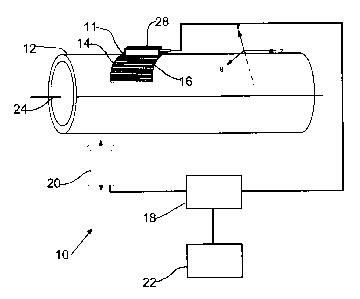
[0016] Referring to FIG. 1, there is shown a blanket probe 10 that is used to
detect the
thickness of a wall that has a non-planar surface, such as a pipe 12 as shown.
Blanket probe
10 has a probe portion 11 comprising a planar substrate, such as a flexible
printed circuit
board 14, which is flexible in one or two dimensions. Referring to FIG. 12, an
array of
detectors 16 is mounted on substrate 14. Preferably, detectors 16 are in a two
dimensional
array, and are detector coils, although other types of detectors known in the
art may also be
used. Detectors 16 are connected to send and receive signals via an interface
18. As will be
discussed, in a preferred embodiment, detectors 16 are sensitive to mutually
orthogonal
electromagnetic fields.
[0017] FIG. 1 through 10 show the various possible configurations that blanket
probe 10
can be used to examine object 12. The actual configuration of blanket probe 10
will depend
on the object being inspected, the preferences of the user, the type of
equipment being used,
and what is being looked for. Objects that may commonly be inspected include a
pipe,
pressure vessel or storage tank. Other suitable objects made may also be
inspected that are
made from suitable metals such as carbon steel, copper, brass, cupro-nickel,
ferritic and other
alloys with a finite thickness. The cross-section of the object may not
necessarily be circular,
but will generally be non-planar. A wired interface 18 between probe portion
11, exciter 20,
and ferroscope 22 is shown, however blanket probe 10 will optionally have a
wireless
interface 18. The details of the interface will be explained below. Probe
portion 11 is
sensitive to magnetic fields in three mutually orthogonal directions shown by
r (radial), 0
(circumferential), and z (axial).
[0018] FIG. 1 shows a possible configuration where probe portion 11 is on one
side of a
CA 02727513 2011-01-06
6
pipe and exciter 20 is on the opposite. Exciter 20 can be opposite the centre
of probe portion
11 or laterally displaced from probe portion 11 as shown. In this
configuration the axis of
exciter coil 20 is perpendicular to the axis 24 of pipe 12.
[0019] FIG. 2 shows a possible configuration where probe portion 11 is on one
side of
pipe 12 and exciter 20 is on the opposite. Exciter 20 is shown as being
laterally displaced
from probe portion 11. In this configuration the axis of exciter 20 is
parallel to axis 24 of pipe
12.
[0020] FIG. 3 shows a possible configuration where probe portion 11 and
exciter coil are
both on the same side of pipe 12. In this configuration the axis of exciter
coil 20 is
perpendicular to axis 24 of pipe 12.
[0021] FIG. 4 shows a possible configuration where probe portion 11 and
exciter coil are
both on the same side of pipe 12. In this configuration the axis of exciter
coil 20 is parallel to
axis 24 of pipe 12.
[0022] FIG. 5 shows a possible configuration where exciter 20 is inside of
pipe 12.
Exciter 20 can be laterally displaced from probe portion 11. In this
configuration the axis of
exciter coil 20 is parallel to axis 24 of pipe 12.
[0023] FIG. 6 shows a possible configuration where exciter 20 is inside of
pipe 12.
Exciter 20 can be laterally displaced from probe portion 11. In this
configuration the axis of
exciter coil 20 is perpendicular to axis 24 of pipe 12.
[0024] FIG. 7 shows a possible configuration where probe portion 11 and
exciter coils
are both on the same side of pipe 12. In this configuration there are multiple
exciter coils 20
(two shown) where the axis of exciter coil 20s is parallel to axis 24 of pipe
12.
[0025] FIG. 8 shows a possible configuration where probe portion 11 and
exciter coils 20
are both on the same side of pipe 12. In this configuration there are multiple
exciter coils
CA 02727513 2011-01-06
7
(two shown) where the axis of exciter coil 20 is perpendicular to axis 24 of
pipe 12.
[0026] FIG. 9 shows a possible configuration where probe portion 11 is on one
side of a
pipe and multiple exciter coils 20 (two shown) are on the other side. In this
configuration the
axis of exciter coils is parallel to axis 24 of pipe 12.
[0027] FIG. 10 shows a possible configuration where probe portion 11 is on one
side of a
pipe and multiple exciter coils 20 (two shown) are on the other side. In this
configuration the
axis of exciter coils is perpendicular to axis 24 of pipe 12.
[0028] Blanket Probe Design - There will now be described a preferred
embodiment of
blanket probe 10. Once the principles of operation are understood, it will be
understood that
modifications to this embodiment, such as the arrangement of components, type
of
components, methods of acquiring data transmitting signals, etc. may be made
while
providing the same functions
[0029] Referring to FIG. 11, a functional block diagram of the major elements
of blanket
probe 10 is shown as a system of instrumentation with a probe portion 11,
interface 18,
exciter unit 21, and operator control & recorder unit 26. Referring to FIG.
12, probe portion
11 contains a rectangular array of 256 magneto-impedance detectors 16 and
sixteen 16-
channel analog multiplexers 28, which are used as line concentrators. The
object being tested
is an insulated pipe 12.
[0030] The operator selects parameters from a software driven menu on a
portable
computer as part of operator control block 26 to set up test conditions and
execute test
instances. The operator's computer 31 (shown in FIG. 24), called the client,
displays
measurement data presenting the progress of tests in real time, which is
displayed on a two-
dimensional color map. Computer 31 also logs test instances placing their
record on a mass
storage media (e.g., memory stick).
[0031] Interface Unit - The interface unit 18 preferably provides a two-way
wireless
access between the operator's computer 31 (client - shown in FIG. 24) and
probe portion 11
CA 02727513 2011-01-06
8
where command information and measurement data are exchanged. Interface 18 may
also
provide a wired connection. The interface unit 18 also preferably provides the
excitation
signal for a remote exciter unit 20 through a wireless link. The purpose for
this arrangement
is to supply an excitation signal while at the same time also provide a
synchronous reference
signal to the lock-in analyzer, a function that is performed by the server
computer 30, which is
part of the interface unit 18.
[0032] The exciter transceiver 86 is permanently in the receive mode to
receive the
excitation signal, the digital signal processor 34 transforms the excitation
signal, which may
be in the form of pulses into a sine wave, and the power amplifier 36 supplies
the necessary
current to drive exciter coil 20, which provides the excitation magnetic
field. FIG. 12 shows
further details of probe portion 11. As shown, probe portion 11 has an array
of 256 magneto-
impedance detectors 16, although other array designs and different numbers of
detectors 16
may also be used.
[0033] Exciter Unit - Exciter unit 21, which powers an exciter coil 20,
consists of
transceiver 86, digital signal processor 42, digital to analog converter 50
and audio frequency
power amplifier 36. The purpose of exciter 20 is to set up an alternating
magnetic field,
whose flux which is conveyed through the ferromagnetic body of the object 12
being tested.
This field is generated by passing a controlled amount of alternating current
at one frequency
or multiple frequencies through a solenoid coil placed adjacent to the wall of
the object 12
being tested. For the case of a pipe, the axis of exciter coil 20 can be
parallel or perpendicular
to the axis of pipe 12. Exciter coil 20 is placed sufficiently far away from
probe portion 11 to
avoid direct coupling; only Through Transmission ("TT") coupling conveyed by
the
ferromagnetic material of the object being tested is the desired arrangement.
Two alternative
exciter implementations are described next.
[0034] Referring to FIG 13, a block diagram of an exciter unit 52 that drives
exciter coil
20 is shown. The exciter current is supplied by an audio amplifier 36 that is
driven by a
digital signal processor 42, which receives a train of rectangular pulses with
a frequency equal
to the excitation frequency from the transceiver 86. The purpose of the
digital signal
processor 42 is to convert the rectangular pulses produced at the output of
transceiver 86 into
CA 02727513 2011-01-06
9
a sequence of binary coded words representing a sine wave. The digital to
analog converter
50, in turn, produces an analog signal to drive the power amplifier 36 from
the coded
waveform. In this instance transceiver 86 permanently remains in the receive
mode. Control
of exciter 20 is exercised through the client computer 31 (shown in FIG. 24)
which sets up
the operational parameters in server computer 30. These features allow
portability of this
instrument, making it useful particularly in confined working conditions. A
diagram of an
exciter unit box 52 is shown in FIG. 14 with amplifier 36, transceiver 86,
signal processor 42
and digital to analog converter 50, a battery 54, BNC connector 56 for an
antenna, an on/off
switch 58, a pilot light 60. Exciter coil 20 may be connected to box 52 using
a connector 62,
such as a four-pin 90 quick-twist BendixTM or LemoTM connector.
[0035] Probe Portion - Referring to FIG. 12, probe portion 11 is constructed
from
flexible printed circuit board 14, which contains an array of detectors 16. In
this illustration,
256 magneto-impedance detectors 16 are arranged in a rectangular array. The
electronic and
mechanical design aspects of probe portion 11 are described below.
[0036] Electrical Design Aspects of Probe Portion - A block diagram in FIG. 15
shows
the interconnection of magneto-impedance detectors 16, analog multiplexers 28,
high-pass
filters 64 (shown in FIG. 21), and a data acquisition system (DAS) 66. The USB
output port
68 of DAS 66 is connected to server computer 30. The circuit is intended for
use with coil or
electronic magnetic field.
[0037] Referring to FIG. 15, a line concentrator 70 consisting of sixteen
analog
multiplexers (first-tier) 28 is used to sequentially connect signals from the
256 detectors 16 in
groups of sixteen to a 16 channel data acquisition system (DAS) 66. Each
multiplexer 28 is
assigned to a row of sixteen detectors 16 and DAS 66 samples the detectors 16
along a
column selected by first-tier multiplexer 28, which shares a common address
bus. Analog
multiplexers 1 to 16 comprise the first-tier multiplexer; the second-tier is
the analog internal
analog multiplexer (not shown) within data acquisition system 66. Columns
containing 16
detectors are selected by the address lines on the first-tier analog
multiplexers 28. The server
computer 30 sequentially addresses columns starting from the column on the far
left and
CA 02727513 2011-01-06
incrementally advancing towards the far right. For each column selected, the
internal analog
multiplexer of data acquisition system 66 sequentially samples along the row
of detectors 16
starting from the top row and incrementally advancing towards the bottom. The
common of
the selector switch of each analog multiplexer is connected to a corresponding
channel of the
5 data acquisition system 66.
[0038] Mechanical Design Aspects of Probe Portion- Referring to FIG. 16, the
side of
the flexible circuit board 14 containing magneto-impedance detectors is
intended to be placed
in close proximity to the surface of the object being tested. The depicted
example contains a
10 square array of 256 detectors 16, where a conducting trace is drawn from
each detector 16
towards one of the four 68-pin SCSI connectors 74. Detectors 16 may be AMI204
detectors
available from Aichi Steel of Japan. Note that axis 24 of the pipe under test
is in the vertical
direction. FIG. 17 shows the top side of the flexible circuit board and
showing the placement
scheme for the 68-pin SCSI connectors 74.
[0039] Referring to FIG. 18, the complete probe portion 11 is shown. The upper
flexible
circuit board 16 contains sixteen analog multiplexers 28 and high-pass filters
(HPF 64 shown
in FIG. 21). Axis 24 of the pipe under test is in the vertical direction. The
68-pin SCSI
connectors 74 at the bottom center makes connection to the data acquisition
system 66.
Flexible circuit board 14 may include stiffeners 75 on either end to only
allow flexibility in
one direction.
[0040] Referring to FIG. 19, in this configuration, a mezzanine board 76 is
used to carry
the analog multiplexers 28, as shown in FIG. 21. Board 76 is rigid, is mounted
above the
detector board 14 and is secured by pins 78 at the top and bottom center of
board 76, which
pass through a stack of mylar sheets 80 where they attach to detector board
16.
[0041] Mylar sheets 80 are used to form a laminate which separates detector
board 14
from mezzanine board 76. This arrangement allows detector board 14 to bend
around the
outer surface of a pipe 12, as shown in FIG. 11. Flexible board 14 contains
256 magneto-
impedance type detectors 16 as shown in FIG. 16. Referring to FIG. 21, rigid
circuit board
76 contains sixteen 16-channel analog multiplexers (first tier) 28 and sixteen
high-pass filters
CA 02727513 2011-01-06
11
64.
[0042] Detectors - Suitable results have been obtained by using Aichi Steel's
AM1204
two-axis magneto-impedance detectors. In pipe examination applications, these
detectors are
capable of measuring the magnetic field along an axis parallel to pipe 12 and
around its
circumference. Other benefits making this type of detector a good choice
include: AMI 204's
are -100 times more sensitive than coil type detectors, and probe portion 11
affords higher
density array than could be formed with coil type detectors. The AMI204 is a
two-axis
magneto-impedance detector capable of measuring magnetic fields in two
mutually
orthogonal directions, both of which are parallel to the planar surface of the
device's package.
The AM1204 magneto impedance detector may be used in a ball grid array (BGA)
package,
which is mounted on a DIP carrier. The AM1204 detector is available in a
surface mount
package, which contains two detector units (one for each direction). Each
detector contains
two magneto-impedance detectors wound with amorphous magnetic wire, a pulse
generator,
logic control circuit, and an instrumentation amplifier. The frequency range
of the measured
magnetic field can vary over the range from a static field to an alternating
field up to 1 kHz.
[0043] First-Tier Multiplexer - Referring to FIG. 20, as mentioned above,
multiplexers
28 are used to perform the switching so that the 256 analog signals from AMI
204 detectors
can be applied to data acquisition system 66 in groups of 16 channels at a
time. This function
is accomplished by first-tier analog multiplexers 28. Each multiplexer 28 is
designated to a
given column containing sixteen detectors 16, and all multiplexers 28 sample a
selected row
of detectors in unison. The data acquisition system 66 has its internal
sixteen channel
multiplexer, which forms the second tier where voltages across a given row of
detectors are
selected. FIG. 20 shows a conceptual schematic diagram for a column containing
sixteen
AMI204 detectors 16 and an analog multiplexer 28. Probe portion 11 has sixteen
of these
columns of detectors 16.
[0044] FIG. 21 shows a drawing of the line concentrator 70 with first-tier
multiplexers
28. The depicted multiplexers 28 may be Analog Devices ADG426 in the SSOP
surface
mount package. A high-pass filter 64 accompanies each multiplexer 28, which is
used as a
CA 02727513 2011-01-06
12
DC block.
[0045] The 68-pin SCSI receptacles 74 on the left and right are interconnected
with short
pieces of ribbon cable 82 (of equal length) to flexible circuit board 14. The
SCSI receptacle
74 on the bottom center is used for making connection to data acquisition
system 66.
[0046] Interface Unit - Referring to FIG. 22, a conceptual drawing of the
physical
layout of interface unit 18 in a box 92 is shown. Interface unit 18 manages
the traffic of data
and control signals to/from operator's computer 31 (shown in FIG. 24). It also
generates the
excitation signal which is also the phase reference for the lock-in detector.
The excitation
signal is sent wirelessly to exciter 20 by the interface unit transceiver 46
to the exciter
transceiver 86. Interface unit 18 is comprised of a data acquisition system
66, an interface
unit transceiver 46, server computer 30, and battery 54.
[0047] The entire blanket probe instrument 10, with exception of exciter 20,
can be
packaged in an aluminum instrument case 92, for example, with the lid (not
shown) of case 92
containing probe portion 11 and its cable. It may also be possible to use the
lid of the case to
contain exciter 20. Each item is firmly secured in place within well fitted
foam
compartments. Blanket probe 10 is preferably operated with the items left in
place. A panel
provides the on/off switch 58, pilot light 60, a multi-pin BendixTM quick
connector 62, and a
BNC connector 56 for antenna or cable. The following sub-sections contain a
brief
description of components within the interface unit.
[0048] Transceiver 46 may be an ACCESTM WM-09-232-020 radio modem which
operates at 9600 baud. It is connected to one of the I/O ports of the server
computer 30 using
a RS-232 nine pin connector (not shown), and operates in the half-duplex mode.
The purpose
of transceiver 46 is to provide a remote means of executing tests and
receiving measurement
data. The transmitter section of the interface unit's transceiver 46 serves
two functions in
separate time intervals: (1) provides a wireless link to exciter 20, and (2)
returns measurement
data to the client computer at the operator's position.
[0049] The data acquisition system 66 may be an ACCES model USB-AI16-16A data
CA 02727513 2011-01-06
13
acquisition system which contains a 16 channel analog multiplexer (second-
tier), 16-bit
analog-to-digital converter, and serial interface using a USB port 67 (shown
in FIG. 15).
[0050] Server 30 is a compact computer which responds to the invigilation of a
test run.
It sets up the DAS operational parameters, records measurement data, performs
data
reduction, and transmits processed data via a radio modem to the client
computer. There are
two important tasks performed by server; these are: respond to the operator's
test condition
selections; and provide digital signal processing functionality (lock-in
analyzer) to reduces the
bulk of measurement data that needs to be transmitted to the client computer
for display and
logging.
[0051] Server 30 is programmed to automatically load set-up test parameters in
the data
acquisition system, and begin to sequentially scan through all columns using
first-tier
multiplexers 28 and channels (rows of detectors) using the second-tier
multiplexer which is an
internal component of the data acquisition system 66. For each row position
selected by first-
tier multiplexers 28, data acquisition system 66 records the voltage
measurement across the
sixteen columns of detectors 16 for a given row position and writes the
corresponding data to
a unique text file. When the test routine has completed, there will be 16 text
files.
[0052] A MatlabTM program may then be used to automatically read the 16 text
files and
apply a digital signal processing algorithm to compute the magnitude and phase
values for all
of the detector positions. This information is stored in a separate text file,
which is later
transmitted from server 30 to the client computer over a pair of radio modems.
The client
receives the processed data and displays results using a two-dimensional color
graphic display
revealing defect location.
[0053] Battery 90 is preferably designed with inverters to efficiently provide
the required
operating voltages for the analog multiplexers, instrumentation amplifiers,
analog-to-digital
converter, micro-controller, modulator (transmitter), and de-modulator
(command receiver).
It is recommended that rechargeable batteries such as Li-ion or gel-cells be
used.
[0054] Operator's Computer and Radio Modem - Referring to FIG. 24, a block
diagram
CA 02727513 2011-01-06
14
of the client computer 31 and transceiver 32, such as a radio modem, is shown.
Test instances
are invigilated by the operator for the client computer 31. A data packet
containing the
frequency of the oscillator, and number of complete cycles that will be
recorded, is preferably
transmitted to server computer 30 between transceivers 32 and 46.
[0055] The operator exercises control of the instrument and displays
measurement data
using a portable (lap-top) computer 31. A modem computer miming for example
WindowsXPTM or LINUXTM is preferably. Lab View (or equivalent) may be used to
generate
control data and record measurement data. A kernel of MATLABTM could be
installed to
perform digital signal processing, statistical analysis, and to display
graphics. This would
allow curve fitting and data interpolation for high quality graphics. The
computer
communicates directly to the interface box through a USB port.
[0056] Results - There will now be described some results that were obtained
using the
embodiment described above.
[0057] Amplitude Measurements - The first part of our research was to
determine
whether only amplitude measurements would be sufficient to determine the
location and
severity of defects. A 6" steel pipe was machined with a 16mm diameter milling
tool to model
external defects. Pipe 12 also had internal defects; these were machined with
a 26mm
diameter mill to model 35 %, 40 %, and 75 % pitting-type wall loss.
[0058] Exciter coil 20 was placed opposite probe portion 11 as shown in FIG.
1. Note
that the axis of the coil is perpendicular to axis 24 of pipe 12. A voltage
was induced on each
detector coil of probe portion 11, which was proportional to the intensity of
the normal
component of the magnetic field on the surface of pipe 12. To equalize the
effect of having a
non-uniform magnetic field distributed over the circumference of pipe 12, the
instrument was
first calibrated on a known-good-pipe.
[0059] A calibration process, written in MatlabTM, was used to obtain
weighting factors
that are used to compensate for the voltage variations among the detector
coils. In our
experiment we recorded five complete cycles of voltage waveform on each coil
and computed
CA 02727513 2011-01-06
their root-mean-square (r.m.s.) values. The r.m.s. value of the voltage on
each detector coil
was computed by MatlabTM and displayed on a two-dimensional display using a
color map to
show the field intensity versus coil position.
5 [0060] FIG. 24 through 26 show examples of the color map used to identify
the location
of 35 %, 40 %, and 75 % outer defects, respectively. The darkness of the color
is represented
by the spacing of the lines. For example, a darker color shows a lower
intensity of magnetic
field in comparison to a bright color. Probe portion 11 was moved to different
locations to
check the sensitivity of various detector coils. FIG. 24 depicts the results
of an amplitude
10 measurement of the 35 % outer defect, where the defect appears in the third
column, second
row. FIG. 25 depicts the results of an amplitude measurement of the 40% outer
defect, where
the defect appears in the second column, third row. FIG. 26 depicts the
results of an
amplitude measurement of the 75 % outer defect, where the defect appears is in
the third
column, second row.
[0061] Outer defects were easily detected using an amplitude measurement
method with
blanket probe 10, however, it was found that internal defects were difficult
to recognize. That
is because external defects have an amplitude variation of 15 % to 25 %
whereas for internal
defects, the variation is an order of magnitude smaller. The phase measurement
method is
therefore preferably, as it is far more sensitive for locating internal
defects.
[0062] Phase Measurement - An important aspect of our design is to develop a
simple
and reliable phase measurement technique that could detect internal defects.
Phase
information was obtained from the Fourier coefficient of the fundamental
component of the
measured signal, which is compared to the phase of the voltage signal of the
other detectors.
[0063] Exciter coil 20 was placed on one side of a steel pipe with probe
portion 11 placed
on the opposite side. It was experimentally determined that exciter coil 20
could be offset by
as much as -23cm from the center of probe portion 11. In that way exciter coil
20 was at a
distance sufficiently removed from probe portion 11 to avoid interference
caused by the
returning lines of magnetic flux. The axis of the coil was perpendicular to
axis 24 of pipe 12.
A calibration was performed on known-good-pipe to determine the phase
relationships of
CA 02727513 2011-01-06
16
every detector within the array with respect to the reference detector.
[0064] FIG. 27 and 28 show examples of a color map used to identify the
location of
50% and 70% internal defects, respectively. Dark colored spots (represented by
closer
spacing of lines) shows large phase change associated with a perturbation of
magnetic field in
the region of an internal defect. FIG. 27 relates to a 50% inner defect with a
16 mm diameter.
the defect appears in the third column and second row. However, in FIG. 28,
which relates
to a 70% inner defect there is ambiguity as to the location of the defect, and
we can only
conclude that it appears somewhere in the third column. To improve
sensitivity, differential
phase measurements may used.
[0065] Differential Phase Measurements - In search of a better measurement
method
that would improve the visibility in locating internal defects, we have
discovered that by
taking differential phase measurements, the resolution is significantly
enhanced over the
relative phase method. Furthermore, a consistent pattern of phase shift over
the defect region
was observed, independent on the size of the defect. FIG. 29 shows a diagram
giving the
location of probe portion 11 and exciter coils 20 on a pipe 12. An oscillator
block 96 is used
to represent the input signal that is amplified by amplifier block 36. In this
situation, probe
portion 11 is represented by two detectors 16a and 16b, which are used to
obtain differential
phase measurements. The pair of adjacent detectors 16a and l6bare placed at
positions A, B,
C, D, and E. The vertical arrow shows the center of the pair of detectors 16a
and 16b.
[0066] Since differences are taken between detectors 16a and 16b, calibration
of the
instrument was not required. The benefit of using the differential phase
measurement method
was first discovered through observations. Over regions of known good pipe, a
constant
phase difference of approximately 2 was measured, which is shown in FIG. 30.
As detectors
16a and 16b approach the periphery of the defect, there is a sharp increase to
6 .
Approximately 1/3 of the way into the defect region a null in phase is
approached. At the
center of the defect region there is a slight phase reversal of approximately
V. FIG. 30 is a
graph showing differential phase versus axial distance on a pipe. The graph
shows
measurements of 70% (line 110) and 30% (line 112) inner defects with 26mm
diameter. The
center line 114 shows the location of the defect in relation to phase
differences. Line 114 on
CA 02727513 2011-01-06
17
the graph shows the location of the defect with respect to data measurements
taken.
[0067] In this patent document, the word "comprising" is used in its non-
limiting sense to
mean that items following the word are included, but items not specifically
mentioned are not
excluded. A reference to an element by the indefinite article "a" does not
exclude the
possibility that more than one of the element is present, unless the context
clearly requires that
there be one and only one of the elements.
[0068] The following claims are to be understood to include what is
specifically
illustrated and described above, what is conceptually equivalent, and what can
be obviously
substituted. Those skilled in the art will appreciate that various adaptations
and modifications
of the described embodiments can be configured without departing from the
scope of the
claims. The illustrated embodiments have been set forth only as examples and
should not be
taken as limiting the invention. It is to be understood that, within the scope
of the following
claims, the invention may be practiced other than as specifically illustrated
and described.