Note: Descriptions are shown in the official language in which they were submitted.
CA 02728697 2010-12-20
WO 2010/000062 PCT/CA2009/000892
132-TRG-01 1286-03PCT
- 1
MULTIPLE-BIT PER CELL (MBC) NON-VOLATILE
MEMORY APPARATUS AND SYSTEM HAVING POLARITY
CONTROL AND METHOD OF PROGRAMMING SAME
CROSS-REFERENCE TO RELATED APPLICATIONS
[001] This application claims benefit to US patent
application 12/166,876 filed July 2, 2008.
TECHNICAL FIELD
[002] The present invention relates generally to non-
volatile memory systems and more specifically to a
nonvolatile multiple-bit per cell (MBC) memory system
having data polarity control.
BACKGROUND
[003] In conventional single-bit per cell memory devices,
the memory cell assumes one of two information storage
states, either an "on" state or an "off" state. The binary
condition of "on" or "off" defines one bit of information.
As a result, a memory device capable of storing n-bits of
data requires (n) separate memory cells.
[004] Increasing the number of bits, which can be stored
using single-bit per cell memory devices depends upon
increasing the number of memory cells on a one-for-one
basis with the number of bits of data to be stored. Methods
for increasing the number of memory bits stored in a memory
device composed of single-bit capacity cells have relied
upon techniques such as manufacturing larger die which
contain more memory cells, or using improved
photolithography techniques to build smaller memory cells.
CA 02728697 2010-12-20
WO 2010/000062 PCT/CA2009/000892
132-TRG-01 1286-03PCT
- 2 -
Reducing the size of a memory cell allows more cells to be
placed on a given area of a single die.
[005] An alternative to single-bit per cell designs is the
storage of multiple-bits of data. in a single memory cell.
One type of memory in which this approach has been followed
is an electrically erasable and programmable device known
as a flash memory cell. In flash cells, programming is
carried out by applying appropriate voltages to the source,
drain, and control gate of the device for an appropriate
time period. This causes electrons to tunnel or be injected
from a channel region to a floating gate. The amount of
charge residing on the floating gate determines the voltage
required on the control gate in order to cause the device
to conduct current between the source and drain regions.
This voltage is termed the threshold voltage, Vth, of the
cell. Conduction represents an "on" or erased state of the
device and corresponds to a logic value of one. An "off" or
programmed state is one in which current is not conducted
between the source and drain regions and corresponds to a
logic value of zero. By setting the threshold voltage of
the cell to an appropriate value, the cell can be made to
either conduct or not conduct current for a given set of
applied voltages. Thus, by determining whether a cell
conducts current at a given set of applied voltages, the
state of the cell (programmed or erased) can be found.
[006] A multiple-bit per cell (MBC) flash memory cell is
produced by creating multiple, distinct threshold voltage
levels within the device. Each distinct threshold voltage
corresponds to a set of data bits. This allows multiple
bits of binary data to be stored within the same memory
cell. When reading the state of the memory cell, each cell
has a binary decoded value corresponding to a value
CA 02728697 2010-12-20
WO 2010/000062 PCT/CA2009/000892
132-TRG-01 1286-03PCT
3 -
dependant upon the conduction of the cell at its present
threshold voltage level. The threshold voltage level for
which the cell compares to a sense amplifier having a pre-
selected input value indicates the bit set representing the
data programmed into the cell. Proper data storage requires
that the multiple threshold voltage levels of a MBC memory
cell be separated from each other by a sufficient amount so
that a level of a cell can be programmed or erased in an
unambiguous manner. The relationship between the data
programmed into the memory cell and the threshold voltage
levels of the cell depends upon the data encoding scheme
adopted for the cells.
[007] In programming a MBC memory cell, the objective is to
apply a programming voltage over a proper time period to
store enough charge in the floating gate to move the
threshold voltage to a desired level. This level represents
a state of the cell corresponding to an encoding of the
data which is to be programmed into the cell. However,
dividing of the threshold voltage range for a two state
(one bit) cell into multiple threshold voltage levels
reduces the margin (threshold voltage difference) between
levels. This necessitates tighter system design tolerances
and reduced programming operation noise margins so that
adjacent levels can be differentiated and programming
errors reduced. However, the tightening of the programming
and read operation threshold voltage windows has led to
slower programming procedures and introduced another
potential source of memory system errors.
[008] U.S. Patent No. 6,937,510 entitled "Non-Volatile
Semiconductor Memory", issued Aug. 30, 2005 to Hosono et
al. which is hereby incorporated by reference, provides a
method and apparatus for programming and reading data from
CA 02728697 2010-12-20
WO 2010/000062 PCT/CA2009/000892
132-TRG-01 1286-03PCT
- 4 -
a non-volatile semiconductor device having multiple-bit per
cell (MBC) memory cells.
[009] However, this method results in an increase in the
number of programming states, which must be traversed,
programming time, and power consumption compared to other
known methods.
[0010] Accordingly, there is a need for the development of
an improved an apparatus, method, and system using a MBC
memory cell as well as non-volatile memory devices and
systems utilizing such improved MBC memory cells.
CA 02728697 2010-12-20
WO 2010/000062 PCT/CA2009/000892
132-TRG-01 1286-03PCT
- 5 -
SUMMARY
[0011] It is an object of the present invention to provide
an apparatus, method, and system using MBC memory cells
that reduce the number of highest programming states used
to program a given field of data.
[0012] According to one aspect of the present invention
there is provided a multiple-bit per cell (MBC) non-
volatile memory apparatus that includes a memory array
having one or more electrically erasable blocks. The blocks
include one or more reprogrammable pages. The
reprogrammable pages include upper and lower pages sharing
common word-lines. The upper and lower pages include
respective upper and lower data fields. The upper and lower
data fields include respective virtual upper and lower
cells of MBC memory cells. The MBC memory cells have
respective threshold voltages programmable to a selected
one of first level, second level, third level, or fourth
level in order from the lowest voltage level. Programming
the lower cells includes programming the respective
threshold voltages from the first threshold voltage level
to the second threshold voltage level. Programming upper
cells includes programming the respective threshold
voltages from the first threshold voltage level to the
fourth threshold voltage level or from the second threshold
voltage level to the third threshold voltage level. The
apparatus also includes a controller for writing data to
the memory array, wherein the controller selectively
inverts data to maximize a number of the bits within a
lower page to be programmed and selectively inverts data to
minimize a number of bits to be programmed in the
respective upper page.
CA 02728697 2010-12-20
WO 2010/000062 PCT/CA2009/000892
132-TRG-01 1286-03PCT
- 6 -
[0013] According to another aspect of the present invention
there is provided a system that includes a multiple-bit
per cell (MBC) non-volatile memory apparatus that includes
a memory array including one or more electrically erasable
blocks. The blocks include one or more reprogrammable
pages. The reprogrammable pages including upper and lower
pages sharing common word-lines. The upper and lower pages
including respective upper and lower data fields. The upper
and lower data fields including respective virtual upper
and lower cells of MBC memory cells. The MBC memory cells
having respective threshold voltages programmable to a
selected one of first level, second level, third level, or
fourth level in order from the lowest voltage level.
Programming the lower cells includes programming the
respective threshold voltages from the first threshold
voltage level to the second threshold voltage level, and
programming upper cells includes programming the respective
threshold voltages from the first threshold voltage level
to the fourth threshold voltage level or from the second
threshold voltage level to the third threshold voltage
level. The memory apparatus also includes a controller for
writing data to the memory array, wherein the controller
selectively inverts data to maximize a number of the bits
within a lower page to be programmed and selectively
inverts data to minimize a number of bits to be programmed
in the respective upper page.
[0014] According to still another aspect if the present
invention there is provided a system that includes a
multiple-bit per cell (MBC) non-volatile memory apparatus
that includes a memory array including one or more
electrically erasable blocks. The blocks include one or
more reprogrammable pages. The reprogrammable pages
including upper and lower pages sharing common word-lines.
CA 02728697 2010-12-20
WO 2010/000062 PCT/CA2009/000892
132-TRG-01 1286-03PCT
7 -
The upper and lower pages including respective upper and
lower data fields. The upper and lower data fields
including respective virtual upper and lower cells of MBC
memory cells. The MBC memory cells having respective
threshold voltages programmable to a selected one of first
level, second level, third level, or fourth level in order
from the lowest voltage level. Programming the lower cells
includes programming the respective threshold voltages from
the first threshold voltage level to the second threshold
voltage level, and programming upper cells includes
programming the respective threshold voltages from the
first threshold voltage level to the fourth threshold
voltage level or from the second threshold voltage level to
the third threshold voltage level. The system also includes
a controller for writing data to the memory array, wherein
the controller selectively inverts data to maximize a
number of the bits within a lower page to be programmed and
selectively inverts data to minimize a number of bits to be
programmed in the respective upper page.
[0015] According to another aspect of the invention there is
provided a method.of programming a lower page and an upper
page in a multi-bit per cell (MBC) non-volatile memory, the
method includes steps of counting a number of bits having a
`0' in a lower data word; inverting all of the bits in the
lower data word if the number of `0' bits is less than half
of a total number of bits in the lower data word;
programming the lower page with the lower data word;
counting a number of bits having a 10' in an upper data
word; inverting all of the bits in the upper data word if
the number of 10' bits is greater than half of a total
number of bits in the upper data word; and programming the
upper page with the upper data word.
CA 02728697 2010-12-20
WO 2010/000062 PCT/CA2009/000892
132-TRG-01 1286-03PCT
8 -
[0016] According to yet another aspect of the present
invention there is provided a method of reading data in a
multi-bit per cell (MBC) non-volatile memory including
steps of sensing threshold voltages of MBC cells within a
page; providing an upper data word by comparing the
threshold voltages to a predetermined voltage reference;
and inverting the upper data word if an upper page polarity
flag is set.
[0017] According to still another aspect of the present
invention there is provided a method of reading data in a
multi-bit per cell (MBC) non-volatile memory including
steps of sensing threshold voltages of MBC cells within a
page; providing a lower data word by comparing the
threshold voltages to two predetermined voltage references;
and inverting the lower data word if a lower page polarity
flag is set.
[0018] In many other publications in this field of art, the
terms single level cell (SLC) and multilevel cell (MLC) are
used to describe cells capable of storing one binary digit
of data or a plurality of binary digits of data
respectively. In this disclosure, for clarity, the terms
single bit per cell (SBC) and multiple-bit per cell (MBC)
are used to describe cells capable of storing one binary
digit of data or a plurality of binary digits of data
respectively.
[0019] It is noted that the representation of binary data
can be arbitrarily assigned to a particular range of
threshold voltage representing a zero (`0') or a one
For convenience, the common convention of assigning an
erased/unprogrammed cell to represent a `1' and a
CA 02728697 2010-12-20
WO 2010/000062 PCT/CA2009/000892
132-TRG-01 1286-03PCT
- 9 -
programmed cell to represent a `0' for an SBC memory cell
is used in this disclosure.
[0020] Also, in this disclosure, an MBC memory cell for
storing M bits per cell has N=2M possible states (State 1,
State 2, ... State n, ... State N-l, State N) . According to
convention, a data value stored in a MBC memory cell by
State n is the ones' complement of the binary Grey Code
representation of n-1 (D = dM_ldM_2...dldo) , wherein do to dm-1
represent the bits stored in a first page to the (M-1)th
page respectively.
[0021] In the particular case where M=2 and N=4, the first
page and second pages are also referred to as the lower
page and upper page respectively. A binary value of `11' is
represented by a first range of threshold voltage of an
erased memory cell or a first state, a binary value of 110'
is represented by a second range of threshold voltage of
the memory cell or a second state, a binary value of 100'
is represented by a third range of threshold voltage of the
memory cell or a third state, and a binary value of 101' is
represented by a fourth range of threshold voltage of the
memory cell or a fourth state in order from the lowest
voltage level.
[0022] The present invention therefore provides a non-
volatile memory device having tighter distribution of
programmed cell threshold voltage (Vth) reduced power
consumption, reduced programming time, and enhanced device
reliability compared to the state of the art heretofore.
CA 02728697 2010-12-20
WO 2010/000062 PCT/CA2009/000892
132-TRG-01 1286-U3 PUT
-
BRIEF DESCRIPTION OF THE DRAWINGS
[0023] Further features and advantages of the present
invention will become apparent from the following detailed
description, taken in combination with the appended
drawings, in which:
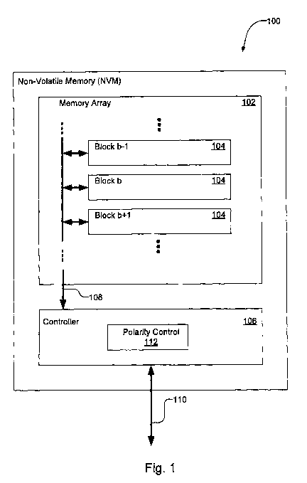
[0024] Fig. 1 is a diagram of a non-volatile memory
apparatus in accordance with the present invention;
[0025] Fig. 2 is a diagram of a block shown in Fig. 1;
[0026] Fig. 3 is a diagram of a page shown in Fig. 2;
[0027] Fig. 4 is a diagram of a Multiple-bit per Cell (MBC)
memory cell shown in Fig. 3;
[0028] Fig. 5 is a diagram of an example threshold voltage
distribution of MBC memory cells shown in Fig. 3;
[0029] Fig. 6 is a diagram showing an alternative
representation of the MBC memory cell shown in Fig. 4;
[0030] Fig. 7 is a diagram showing a alternative
representation of the page shown in Fig. 3;
[0031] Figs. 8a to 8c are diagrams of example threshold
voltage distributions of MBC memory cells of the page shown
in Fig. 3;
[0032] Fig. 9 is a flowchart of a method of programming data
words into a lower page and an upper page in accordance
with the present invention;
[0033] Fig. 10 is a more detailed flowchart of the method
shown in Fig. 9;
CA 02728697 2010-12-20
WO 2010/000062 PCT/CA2009/000892
132-TRG-01 1286-03PCT
- 11 -
[0034] Figs. 11 and 12 are flowcharts of steps in the method
shown in Fig. 10;
[0035] Figs. 13 and 14 are flowcharts of methods of reading
data in accordance with the present invention;
[0036] Fig. 15 is a diagram of a memory system including the
non-volatile memory apparatus shown in Fig. 1 in accordance
with the present invention;
[0037] Fig. 16 is a diagram of a non-volatile memory
apparatus in accordance with the present invention;
[0038] Fig. 17 is a diagram of a memory system including the
non-volatile memory apparatus shown in Fig. 16 in
accordance with the present invention;
[0039] Fig. 18 is a diagram of a non-volatile memory
apparatus in accordance with the present invention;
[0040] Fig. 19 is a diagram of a memory system including the
non-volatile memory apparatus shown in Fig. 18 in
accordance with the present invention;
[0041] Fig. 20 is a diagram of a non-volatile memory
apparatus in accordance with the present invention;
[0042] Fig. 21 is a diagram of a memory system in accordance
with the present invention including the non-volatile
memory apparatus shown in Fig. 20 in accordance with the
present invention; and
[0043] Figs. 22A to 22D are diagrams of electric devices
including the memory systems shown in Figs. 15, 17, 19, and
21 respectively.
CA 02728697 2010-12-20
WO 2010/000062 PCT/CA2009/000892
132-TRG-01 1286-03PCT
- 12 -
[0044] It will be noted that throughout the appended
drawings, like features are identified by like reference
numerals.
CA 02728697 2010-12-20
WO 2010/000062 PCT/CA2009/000892
132-TRG-01 1286-03PCT
- 13 -
DETAILED DESCRIPTION OF THE EMBODIMENTS
[0045] Referring first to Fig. 1, there is shown a diagram
of a non-volatile memory (NVM) apparatus 100 in accordance
with the present invention. The memory apparatus 100 is
preferably a Flash memory but may be any type of EEPROM
(Electrically Erasable Programmable Read-Only Memory) . The
memory apparatus includes at least one memory array 102
that includes one or more memory blocks 104. For the
purpose of this disclosure a block is defined as an
erasable section of memory.
[0046] The memory apparatus 100 also includes a controller
106 for controlling the functions of the memory array such
as executing commands received on an interface 110, writing
data received on the interface 110 to the memory array 102,
reading data from the memory array 102 and providing the
data to the interface 110, and erasing data from the blocks
104. The controller 106 includes a polarity control 112
function which will be described in detail herein below. It
should be noted that the polarity control 112 may be
implemented in hardware, software, firmware, or any
combination thereof and still be within the scope of the
invention.
[0047] For convenience and clarity, interconnect 108 between
the memory array 102 and the controller 106 is shown as a
simplified schematic representation 108. This interconnect
108 includes conventional memory architecture such as row-
decoders, word-lines, bit-lines, column-decoders, page
buffers, and sense amplifiers which are well understood by
those skilled in the art.
[0048] Referring to Fig. 2, there is shown further details
of the block 104 shown in Fig. 1. The block 104 includes at
CA 02728697 2010-12-20
WO 2010/000062 PCT/CA2009/000892
132-TRG-01 1286-03PCT
- 14 -
least one page 202. For the purpose of this disclosure a
page is defined as a writable section of memory. A word or
data word is defined as binary number that can be stored in
a page. The parameter j is defined as the width of a data
word/page.
[0049] Referring to Fig. 3, there is shown further details
of a page 202 shown in Fig. 2. The page 202 includes a data
field 302 and a spare field 304. The data field 302
includes a plurality of Multi-Bit per Cell (MBC) memory
cells 306. The spare field 304 includes a polarity flag 308
that will be described further herein below and a
conventional error correction code (ECC) 310.
[0050] Referring to Fig. 4 there is shown an MBC memory cell
shown 306 shown in Fig. 3. A threshold voltage 402 of the
MBC memory cell 306 is programmable to one of N
predetermined threshold voltages. In this example
embodiment N is chosen to be 4. The four predetermined
threshold voltages 404,406,408,410 corresponding to states
1 to 4 from the lowest to highest value.
[0051] In Fig. 5 there is shown an example distribution
diagram of the threshold voltages 402 of a page 202. The y-
axis 502 represents a number of cells programmed to each
state 404,406,408,410 and the x-axis 504 represents
threshold voltage (Volts) corresponding to each state
404,406,408,410. In this example, the MBC memory cells 202
are about evenly distributed over the four predetermined
threshold voltages 404,406,408,410. The threshold voltages
preferably have a small deviation from the ideal
predetermined values and have enough margin from adjacent
reference voltages VRefl, VRef2, VRef3 506, 508, 510 to provide
reliable operation. The asymmetrical predetermined
CA 02728697 2010-12-20
WO 2010/000062 PCT/CA2009/000892
132-TRG-01 1286-03PCT
- 15 -
reference voltages 506,508,510 is one example of a
conventional threshold voltage scheme. The present
invention is also applicable to other threshold voltage
schemes such as the scheme described in applicant's co-
pending U.S.: application no.: 2008/0062760, titled: "FLASH
MULTI-LEVEL THRESHOLD DISTRIBUTION SCHEME", by Kim, Filed:
Jun. 13, 2007, which is hereby incorporated by reference.
[0052] The representation of the MBC cell 306 shown in Fig.
4 is a schematic representation physical hardware.
Alternatively, the MBC cell 306 can be represented as shown
in Fig. 6. In this example, the four states 404,406,408,410
of the MBC memory cell 306 are represented as two virtual
SBC (single bit per cell) cells 602,604 each having one bit
per cell. In general, where the number of states in a MBC
memory cell is N, the number of virtual cells having one
bit per cell is M=1og2N and N is preferably chosen to be an
integer power of 2. In the embodiment described here, N=4
and M=2. The lower cell 602 and an upper cell 604 are
addressable using two different row-addresses.
[0053] Furthermore, as shown in Fig. 7, the page 202 shown
in Fig. 3 can be represented as including a virtuallower
page 702 and a virtual upper page 712 which can be
addressed independently using the two different row-
addresses. The lower page 702 and upper page 712 include a
respective lower data field 704 and upper data field 714 as
well as a respective lower spare field 706 and upper spare
field 716. The lower data field 704 and upper data field
714 include a respective plurality (j) of lower cells 602
and upper cells 604. The lower spare field 706 and upper
spare field 712 include a respective lower page polarity
flag 708 and upper page polarity flag 718 as well as a
respective lower ECC 710 and upper ECC 720.
CA 02728697 2010-12-20
WO 2010/000062 PCT/CA2009/000892
132-TRG-01 1286-03PCT
- 16 -
[0054] Furthermore still, a plurality of lower pages 702
within a block 102 may be referred to as an lower plane
(not shown) and a plurality of upper pages 712 within a
block 102 may be referred to as an upper plane (not shown).
This is known as a dual-plane or more generally a multi-
plane architecture in the art wherein each plane can be
addressed independently even though physically sharing the
same row-decoders, word-lines, and cells.
[0055] When a block 104 is erased, all MBC memory cells 306
in the block are set to State 1 404. State 1 404
corresponds to cells that have been erased and are assigned
the data value `11' by convention. State 2 406 corresponds
to a data value of 110', State 3 408 corresponds to a data
value of `00', and State 4 410 corresponds to a data value
of '01'.
[0056] Programming (storing a `0') the lower cell 602
includes steps of programming the MBC cell 306 from State 1
404 to State 2 406. Programming the upper cell 604 includes
steps of programming the MBC cell 306 from State 1 404 to
State 4 410 or from State 2 406 to State 3 408.
[0057] In general, programming the mtn cell of the M virtual
cells includes steps of programming the MBC cell 306 from
one of states 1, 2, to 2m-1 to one of states 2m, 2m-1,
to 2m+l+l respectively.
[0058] Fig. 8a to 8c show example distributions 802,804,806
of a page 202 after erase and write operations. In Fig. 8a
all of the cells 306 are in State 1 404 after being erased.
In Fig. 8b there is shown a distribution 804 after the
lower data field 704 has been programmed 512 with a data
word wherein the data word has a different number of 10's
than `1's. Note, as described further herein below, more
CA 02728697 2010-12-20
WO 2010/000062 PCT/CA2009/000892
132-TRG-01 1286-03PCT
- 17
cells 306 are programmed 512 to State 2 406 than left in
State 1 404. In Fig. 8c there is shown a distribution 806
after the upper data field 714 has been programmed 514,516
with a data word wherein the data word has a different
number of `0's than `l's. Note, as further described herein
below, fewer cells 306 are programmed 514,516 to States 3
and 4 408,410 from States 2 and 1 406,404 respectively. It
should also be noted that State 4 410 in Fig. 8c has the
lowest number of cells when compared to States 1 to 3
404,406,408.
[0059] In Fig, 9 there is shown a flow chart 900 of a method
of programming data words into a lower page 702 and an
upper page 712 in accordance with the present invention.
The method includes a step 902 for programming a lower page
702 with more 10's than `l's by selectively inverting the
data word to be programmed into the lower page 702; and a
step 904 for programming an upper page 712 with more `l's
than `0's by selectively inverting the data word to be
programmed into the upper page 712. It should be noted that
a dotted line 903 between steps 902 and 904 means that in
is not necessary to program an upper page 712 immediately
after programming the corresponding lower page 702. For
example, a plurality of lower pages 702 within a block 104
may be programmed before the corresponding upper pages 712
are programmed and still be within the scope of the
invention.
[0060] Fig. 10 is a more detailed flowchart 1000 of the
method depicted by the flowchart 900 shown in Fig. 9. The
step of programming the lower page 902 includes steps of:
counting 1002 a number of `0's in a data word to be
programmed into the lower page 702; deciding 1004 if the
lower data word has fewer `0's than `l's or alternatively
CA 02728697 2010-12-20
WO 2010/000062 PCT/CA2009/000892
132-TRG-01 1286-03PCT
- 18 -
less than j/2 (half the word/page width); if yes, setting
1006 a lower page polarity flag 708, and inverting 1008 the
lower data word; if no, clearing 1012 the lower page
polarity flag 708; and programming 1010 the lower data word
into the lower page 702 (described in further detail herein
below). The step of programming the upper page 904 includes
steps of: counting 1014 a number of 10's in a data word to
be programmed into the upper page 712; deciding 1016 if the
upper data word has more `0's than `1's or alternatively
greater than j/2; if yes, setting 1018 an upper page
polarity flag 718, and inverting 1020 the upper data word;
if no, clearing 1024 the upper page polarity flag 718; and
programming 1010 the upper data word into the upper page
712 (described in further detail herein below).
[0061] Fig. 11 is a flowchart of the step 1010 for
programming the lower data word into the lower page 702 of
the method depicted by the flowchart 1000 shown in Fig. 10.
For each bit in the data word to be programmed 1102, if the
data bit is a `1' then inhibit programming 1104 or leave it
in State 1 404; if the data bit is a `0' then program 512
the cell from State 1 404 to State 2 406.
[0062] Fig. 12 is a flowchart of the step 1022 for
programming the upper data word into the upper page 712 of
the method depicted by the flowchart 1000 shown on Fig. 10.
First, a lower data word is read from the lower page 702
sharing the same word-line as the upper page 712. Then for
each bit in the lower data word and upper data word, if the
upper/lower data bits are 111' 1204,1206 then programming
is inhibited 1208 and the cell remains in State 1 404; if
the upper/lower data bits are 110' 1204,1206 then the cell
is programmed 516 from State 1 406 to State 4 410; if the
upper/lower data bits are `01' 1204,1212 then programming
CA 02728697 2010-12-20
WO 2010/000062 PCT/CA2009/000892
132-TRG-01 1286-03PCT
19 -
is inhibited 1214 and the cell remains in State 2 406; else
if the upper/lower data bits are `00' 1204,1206 the cell is
programmed 514 from State 2 406 to State 3 408.
[0063] Fig. 13 is a flowchart 1300 of a method of reading
data from an upper page 712 in accordance with the present
invention. First, a threshold voltage 402 is sensed 1302
from each cell 306 in the page 202; if the threshold
voltage is not greater than VRef2 1304 and the polarity flag
is not set 1306 then the upper bit is a `1' 1310; if the
threshold voltage is not greater than VRef2 1304 and the
polarity flag is set 1306 then the upper bit is a `0' 1308;
if the threshold voltage is greater than VRef2 1304 and the
polarity flag is not set 1307 then the upper bit is a 10'
1308; else if the threshold voltage is greater than VRef2
1304 and the polarity flag is set 1307 then the upper bit
is a `1' 1310.
[0064] Fig. 14 is a flowchart 1400 of a method of reading
data from a lower page 702 in accordance with the present
invention. First, a threshold voltage 402 is sensed 1402
from each cell 306 in the page 202; if the threshold
voltage is less than VRefl or greater than VRef3 1404 and the
polarity flag is not set 1406 then the lower bit is a 11'
1410; if the threshold voltage is less than VRefl or greater
than VRef3 1404 and the polarity flag is set 1406 then the
upper bit is a 10' 1408; if the threshold voltage is
greater than VRefl and less than VRef3 1404 and the polarity
flag is not set 1407 then the upper bit is a `0' 1408; else
if the threshold voltage is greater than VRef1 and less than
VRef3 1404 and the polarity flag is set 1407 then the upper
bit is a `1' 1410.
CA 02728697 2010-12-20
WO 2010/000062 PCT/CA2009/000892
132-TRG-01 1286-03PCT
- 20 -
[0065] In general, a threshold voltage of the MBC cell is
sensed in a conventional manner, if the sensed threshold
voltage is less than VRefl then the value stored is N-1 (all
`l's, or ones' complement of Grey code representation of
0) , if the sensed threshold voltage is between VRef (n-1) and
VRefn then the value stored in the MBC cell is the ones'
complement of the Grey code representation of n-1, and if
the sensed threshold voltage of the MBC memory cell is
greater than VRef (N-1) then the value, stored is the ones'
complement of the Grey code representation of N-1.
Furthermore, if a corresponding polarity flag is set then
the value read from the MBC cell is inverted.
[0066] The M virtual pages can be read f rom the Mth page to
the first page sequentially in order. For reading the Mth
page the threshold voltages are compared to VRef (2M-1) ; then
for reading the (M-1)th page the threshold voltages are
compared to VRef (2M 2 ) and VRef3 (2M 2 ) ; then for reading the (M-
,
2) th page the threshold voltages are compared to VRef (2M-3
VRef3 (2M 3 ) , VRef5 (2M 3 ) , and VRef7 (2M 3) ; and so on until the first
where the threshold voltages are compared to VRefl, VRef3,
VRef5, ... VRef (N-1)
[0067] Fig. 15 is a diagram of a memory system 1500 in
accordance with the present invention. The system 1500
includes a memory controller 1502 that has a host interface
1504 and a parallel bus interface for connecting to one or
more nonvolatile memories 100 having polarity control 112
as described herein above.
[0068] Referring next to Figs. 16 and 17 there is shown
another non-volatile memory apparatus 1600 and system 1700
in accordance with the present invention wherein a
controller 106 is adapted to communicate over a system bus
CA 02728697 2010-12-20
WO 2010/000062 PCT/CA2009/000892
132-TRG-O1 1286-03PCT
- 21 -
1506 with a memory controller 1702 having polarity control
112.
[0069] In Figs. 18 and 19 there is shown another non-
volatile memory apparatus 1800 and system 1900 in
accordance with the present invention. The non-volatile
memory apparatus 1800 is substantial the same as the one
100 shown in Fig. 1, except that it has a serial input 1802
and a serial output 1804 instead of a parallel interface
110. The memory system 1900 includes one or more of the
non-volatile memory apparatus 1800 shown in Fig. 18. A
memory controller 1902 having a host interface 1504, a
serial output 1904 and a serial input 1906 controls the
memory system 1900 in a manner, for example, as described
in applicant's co-pending U.S. application titled:
"MULTIPLE INDEPENDENT SERIAL LINK MEMORY", no: 11/324,023,
filed: Dec. 30, 2005 by Kim et al which is hereby
incorporated by reference.
[0070] Figs. 20 and 21 show another non-volatile memory
apparatus 2000 and system 2100 in accordance with the
present invention wherein a controller 106 is adapted to
communicate over a serial bus 1904,1906 with a memory
controller 2102 having polarity control 2104. The non-
volatile memory apparatus 2000 is substantial the same as
the one 1600 shown in Fig. 16, except that it has a serial
input 1802 and a serial output 1804 instead of a parallel
interface 110. The memory system 2100 includes one or more
of the non-volatile memory apparatus 2000 shown in Fig. 20.
A memory controller 2102 having a host interface 1504, a
serial output 1904 and a serial input 1906 controls the
memory system 2100 in a manner, for example, as described
in application no.: 11/324,023, supra.
CA 02728697 2010-12-20
WO 2010/000062 PCT/CA2009/000892
132-TRG-01 1286-03PCT
- 22 -
[0071] It should be noted that while embodiments of system
having parallel interfaces (Figs. 15 and 17) and serial
interfaces (Figs. 19 and 21), systems having any
combination of parallel and serial interfaces are also
within the scope of the invention.
[0072] While embodiments including MBC memory cells having 2
bits per cell have been described, the present invention is
also applicable to apparatus, methods, and systems
including MBC memory cells having greater than 2 bits per
cell.
[0073] In general, referring again to Fig. 4, an MBC memory
cell 306 having M bits per cell includes N states (State 1,
State 2, ... State n, ... State N-l, State N) from the lowest
to the highest value of Vth in order, wherein ,see Fig. 5,
State n represents a data value (D) that is a 1's
complement of the Gray Code value of n-1 (n=1 to N) , and
wherein the LSB (least significant bit) of D to the MSB
(most significant bit) of D represent data stored in
virtual cells. Programming the mth bit of D into the mth
virtual cell includes programming the MBC memory cell from
one of states 1, 2, ... 2m-1 to one of states 2m, 2m-1, ... 2m-
1+1 respectively.
[0074] A controller selectively inverts polarity of data to
be programmed to maximize a number of bits to be programmed
within each one of pages 1 to M-1 and selectively inverts
the polarity of the data to be programmed to minimize a
number of bits to be programmed within the Mth page.
[0075] As described herein above the memory systems shown in
Figs. 15, 17, 19, and 21 may also be embedded, as shown in
Figs. 22A, 22B, 22C, and 22D respectively, in an electric
device 2200. The electric device 2200 may be, for example,
CA 02728697 2010-12-20
WO 2010/000062 PCT/CA2009/000892
132-TRG-01
- 23 1286-03PCT
-
a memory stick, a solid state disk (SSD), a laptop
computer, a desktop computer, a personal digital assistant
(PDA), audio player, or the like where the advantages of
embodiments of the present invention as described herein
are especially beneficial.
[0076] Therefore the present invention provides an
apparatus, method, and system for programming a multiple-
bit per cell memory cell that reduces the number of highest
programming states used to program a given field of data
and hence provides a non-volatile memory device having
tighter distribution of programmed cell threshold voltage
(Vth), reduced power consumption, reduced programming time,
and enhanced device reliability compared to the state of
the art heretofore.
[0077] The embodiments of the invention described above are
intended to be exemplary only. The scope of the invention
is therefore intended to be limited solely by the scope of
the appended claims.
CA 02728697 2010-12-20
WO 2010/000062 PCT/CA2009/000892
132-TRG-01
- 24 1286-03PCT
Table of Elements
Element Name Reference Number
Non-Volatile Memory 100
Apparatus
Memory Array 102
Block 104
Controller 106
Interconnection 108
Interface 11.0
Polarity Control 112
Page 202
Data Field 302
Spare Field 304
MBC Memory Cell 306
Polarity Flags 308
Error Correction Code 310
(ECC)
Threshold Voltage 402
States/Threshold Voltages 404,406,408,410
1 to 4
Example Threshold Voltage 500
Distribution
Vertical Axis, Number of 502
Cells
Horizontal Axis, Voltage 504
Reference Voltages 1 to 3 506,508,510
Program From State 1 to 2 512
Program From State 2 to 3 514
Program From State 1 to 4 516
Lower Bit 602
Upper Bit 604
Lower Page 702
Lower Data Field 704
Lower Spare Field 706
Lower Polarity Flag 708
CA 02728697 2010-12-20
WO 2010/000062 PCT/CA2009/000892
132-TRG-01 1286-03PCT
- 25 -
Element Name Reference Number
Lower ECC 710
Upper Page 712
Upper Data Field 714
Upper Spare Field 716
Upper Polarity Flag 718
Upper ECC 720
Threshold Voltage 802,804,806
Distribution
Method of Programming 900
Flowchart
Program Lower Page 902
Disconnect between 902 and 903
904
Program Upper Page 904
Detailed Method of 1000
Programming Flowchart
Steps for Programming 1002 to 1012.
Lower Page
Steps for Programming 1014 to 1024
Upper Page
Steps for Programming 1102 to 1104
Lower Data Word
Steps for Programming 1202 to 1214
Upper Data Word
Reading Upper Data Word 1300
Flowchart
Steps for Reading Upper 1302 to 1310
Data Word
Reading Lower Data Word 1400
Flowchart
Steps for Reading Lower 1402 to 1410
Data Word
Memory System 1500
Memory Controller 1502
Host Interface 1504
Parallel Bus 1506
Non-Volatile Memory 1600
CA 02728697 2010-12-20
WO 2010/000062 PCT/CA2009/000892
132-TRG-01 1286-03PCT
- 26 -
Element Name Reference Number
Memory System 1700
Memory Controller w/ 1702
Polarity Control
Non-Volatile Memory w/ 1800
Serial Interface
Serial Input Interface 1802
Serial Output Interface 1804
Memory System w/ Serial 1900
Interconnect
Memory Controller w/ 1902
Serial Interface
Serial Output 1904
Serial Input 1906
Non-Volatile Memory w/ 2000
Serial Interface
Memory System 2100
Memory Controller w/ 2102
Serial Interface and
Polarity Control
Electric Device 2200