Note: Descriptions are shown in the official language in which they were submitted.
CA 02730229 2011-01-07
WO 2010/005983 PCT/US2009/049832
PROPERTY MODULATED MATERIALS AND METHODS OF MAKING THE SAME
FIELD OF THE DISCLOSURE
The disclosure relates generally to layered, such as, for example,
nanolayered, or graded
materials and methods of making them. The disclosure also relates generally to
articles
produced from the layered or graded materials.
BACKGROUND
In general, today's advanced material applications are subjected to
environments and stre sses,
which benefit from combinations of material properties. For example, in
ballistic applications, a
material is sought which is lightweight and thus fuel efficient, while at the
same time provides
great impact absorption properties to prevent injury or mechanical failure to
an underlying
structure that may be the target of shrapnel or an exploding device. In
aircraft or seacraft
applications, materials that are strong, light-weight and at the same time
corrosion resistant are
also sought. In an attempt to achieve these and other material property
combinations, composite
materials (i.e., multiphase materials) are employed.
There are many types of composite materials. For example, particle-reinforced
composite
materials, fiber-reinforced composite materials, structural composite
materials or layered
composite materials are generally well-known. Each type of composite material
can include two
or more phases wherein one phase makes up the majority of the material and is
know as the
matrix material and the second phase (and potentially additional phases)
make(s) up a lesser
extent of the composite and can be dispersed within the matrix material or
layered within the
matrix material to form a sandwich. The presence of the second and additional
phases affects the
material properties (such as, for example, the mechanical and thermal
properties) of the
composite material. That is, the material properties of the composite material
are dependent
upon the material properties of the first phase and the second phase (and
additional phases) as
well as the amounts of the included phases forming the composite. Thus,
material properties of a
composite can be tailored for a specific application by the selection of
specific concentrations of
the phases, as well as potentially, the sizes, shapes, distribution, and
orientation of the included
phases.
Difficulties in the formation, durability, and tailoring of material
properties have however
impeded or prevented the use of composite materials in some applications. For
example,
material failure may be due, at least in part, to abrupt property changes
along phase interfaces.
CA 02730229 2011-01-07
WO 2010/005983 PCT/US2009/049832
-2-
GLOSSARY AND SUMMARY
The following terms are used throughout this disclosure.
"Composite" is a material including two or more distinct characteristics or
phases. For example,
a material which includes a layer or zone of a first
microstructure/nanostructure together with a
layer or a zone of a second or different microstructure/nanostructure is
considered a composite
for purposes of this disclosure.
"Property Modulated Composite" defines a material whose structural,
mechanical, thermal,
and/or electrical properties can be represented by a period function of one or
more space
coordinates, such as, for example, a growth direction of the material.
"Electrodeposition" defines a process in which electricity drives formation of
a deposit on an
electrode at least partially submerged in a bath including a component or
species, which forms a
solid phase upon either oxidation or reduction.
"Electrodepositable Species" defines constituents of a material deposited
using
electrodeposition. Electrodeposited species include metal ions forming a metal
salt, as well as
particles which are deposited in a metal matrix formed by electrodeposition.
Polymers, metal
oxides, and intermetallics can also be electrodeposited.
"Waveform" defines a time-varying signal.
The present disclosure relates to property modulated materials. More
particularly, the present
disclosure relates to a material electrodeposited to include layers or zones
of property modulated
bulk material. Property modulation is achieved through nanostructure and
microstructure
(collectively referred to herein as "nanostructure") modulation during a
deposition process.
These "Nanostructure Modulated Composites" (NMCs) are comprised of layers with
distinct
nanostructures (each nanostructure has its own distinct phase to form a
composite), where the
nanostructure may be defined by grain size (i.e., average grain size), grain
orientation, crystal
structure, grain boundary geometry, or a combination of these. That is, the
NMCs are formed
from a single bulk material (e.g., Fe, an alloy of Ni and Fe, a polymer, a
metal including ceramic
CA 02730229 2011-01-07
WO 2010/005983 PCT/US2009/049832
-3 -
particles) deposited to include adjacent layers which have a distinct
nanostructure (e.g., a first
layer of large grain size Fe adjacent to a second layer including small grain
size Fe).
"Nanostructure Graded Composites" (NGCs) are materials which display a
nanostructure
gradient in a given direction. NGCs are similar to NMCs except that the
nanostructured layers in
the latter case are diffuse in a NGC so that there are no distinct interfaces
between layers. That
is, instead of having distinct layers, NGCs have difuse or combination regions
between sections
or zones defined by a particular nanostructure.
In embodiments, the present disclosure provides an electrodeposition process
to produce NMCs
and NMGs. In embodiments, a layered material can be created by varying the
appropriate
electrodeposition parameter at predetermined intervals during the course of
deposition.
Embodiments described herein provide processes for the production of NMC and
NGC having
predetermined layers or gradients.
Embodiments described herein also provide property modulated alloys comprising
layers in
which each layer has a distinct mechanical or thermal property and where that
distinct property is
achieved by controlling the nanostructure of the layer during deposition.
Embodiments described herein also provide bulk materials produced from NMCs
and/or NGCs,
where the bulk materials have overall mechanical, thermal, and/or electrical
properties that are
achieved as a result of the combined mechanical, thermal, and/or electrical
properties of the
individual layers comprising the NMC and/or NGC.
Other embodiments provide articles produced from NMCs and/or NGCs, where the
articles have
overall mechanical, thermal, and electrical properties that are achieved as a
result of the
combined mechanical, thermal, and electrical properties of the individual
layers comprising the
NMC and/or NGC.
Other embodiments provide NMCs and NGCs comprising a plurality of alternating
layers of at
least two distinct microstructures in which at least one microstructure layer
thickness is varied in
a predetermined manner over the overall thickness of the alloy.
CA 02730229 2011-01-07
WO 2010/005983 PCT/US2009/049832
-4-
Embodiments described herein also provide processes for production of
continuously graded
alloys in which the relative concentrations of specific microstructure
elements (such as grain
size, crystal orientation or number of dislocation sites) varies throughout
the thickness of the
alloy. Such alloys may be produced, for example, by slowly changing the
appropriate
electrodeposition parameter (such as, for example temperature) during
deposition rather than by
rapidly switching from one deposition condition (in this case temperature), to
another.
In NMCs and NGCs, properties of commercial interest may be achieved by varying
the layer
thickness and structure. For example, by electroforming a metal or an alloy
whose microstructure
varies from amorphous (single nanometer grains) to crystalline (multi-micron
size grains) a
material may be created having a predetermined gradient in hardness.
In general, in one aspect, embodiments herein provide methods for producing a
property
modulated composite utilizing electrodeposition. The method includes providing
a bath
including at least one electrodepositable species; providing a substrate upon
which the at least
one electrodepositable species is to be electrodeposited; at least partially
immersing said
substrate into the bath; and changing one or more plating parameters in
predetermined durations
between a first value and a second value. The first value produces a first
material having a first
composition and a first nanostructure defined by one or more of a first
average grain size, a first
grain boundary geometry, a first crystal orientation, and a first defect
density. The second value
produces a second material having a second composition and a second
nanostructure defined by
one or more of a second average grain size, a second grain boundary geometry,
a second crystal
orientation, and a second defect density, wherein the first and second
compositions are the same,
while the first nanostructure differs from the second nanostructure. (That is,
one or more of the
first average grain size, first grain boundary geometry, first crystal
orientation and first defect
density differs from the second average grain size, second grain boundary
geometry, second
crystal orientation and second defect density.)
Such embodiments can include one or more of the following features. The one or
more plating
parameters utilized in the methods can be selected from the group consisting
of temperature, beta
(B), frequency, peak to peak current density, average current density, duty
cycle, and mass
transfer rate. In embodiments, the more than one plating parameters can be
changed between the
first value and the second value. For example, two or more (e.g., 2, 3, 4)
plating parameters can
be changed. In one embodiment, both beta and temperature are changed (e.g.,
plating parameters
CA 02730229 2011-01-07
WO 2010/005983 PCT/US2009/049832
-5-
B1, Ti are utilized during a first period of time and B2, T2 are utilized
during a second period of
time). More than two values of the plating parameters can be utilized in
methods in accordance
with the disclosure. For example, in a method in which temperature (T) is
varied, the method
may apply two or more (e.g., 2, 3, 4, 5, 6, etc.) values of temperature (e.g.,
Ti, T2, T3, T4, T5,
T6) can be utilized. The changing of the one or more plating parameters
between a first value
and the second value can include varying the one or more plating parameters as
a continuous
function of time (i.e., as a waveform, such as a sine wave, a triangle wave, a
sawtooth wave, a
square wave, and combination thereof). The first and second materials can be
one or more of a
metal (e.g., nickel, iron, cobalt, copper, zinc, manganese, platinum,
palladium, hathium,
zirconium, chromium, tin, tungsten, molybdenum, phosphorous, barium, yttrium,
lanthanum,
rhodium, iridium, gold and silver), a metal oxide, a polymer, an
intermetallic, a ceramic (e.g.,
tungsten carbide) and combinations thereof. The method can be utilized to
produce a layered
property modulated composite. Alternatively, the method can be used to produce
a graded
property modulated composite. In these property modulated composites the
layers (for layered)
or sections (for graded) include different mechanical properties, thermal
properties, and/or
electrical properties between adjacent layers or sections. For example in a
layered property
modulated composite, a first layer can include a first mechanical property
(such as, for example,
a high hardness, low ductility) and a second layer can include a second
mechanical property
(such as, for examples, low hardness, but high ductility). Examples of
mechanical properties
which can differ between layers or sections include, for example, hardness,
elongation, tensile
strength, elastic modulus, stiffness, impact toughness, abrasion resistance,
and combinations
thereof Examples of thermal properties which can differ between layers or
sections include,
coefficient of thermal expansion, melting point, thermal conductivity, and
specific heat. For the
layered property modulated composites, each layer has a thickness. The
thickness of the layers
can be within the nanoscale to produce a nanolaminate (e.g., thickness of each
layer is about 1
nm to about 1,000 nm, 10 nm to 500 nm, 50 nm to 100 nm thick, 1 nm to 5 nm).
Each layer in
the nanolaminate can be substantially similar in thickness. Alternatively, the
thickness of the
layers can vary from one layer to the next. In some embodiments, the
thicknesses are greater
than 1,000 nm (e.g., 2,000 nm, 5,000 nm, 10,000 nm).
An advantage of embodiments described herein is the control of the mechanical
and thermal
properties of a material (e.g., mechanical properties, thermal properties) by
tailoring inter-grain
boundaries or grain boundary orientations. For example, by modulating the
orientation and grain
geometry at the grain boundaries, a bulk material may be produced which
resists deformation in
CA 02730229 2011-01-07
WO 2010/005983 PCT/US2009/049832
-6-
several ways. For example, without wishing to be bound by theory, it is
believed that in
structures that contain large, aligned crystals, slippage will occur,
resulting in a ductile material.
In another example, by interleaving layers comprising amorphous
microstructures or
polycrystalline structures, a harder and more brittle layer may be realized.
These layers may be
very strong and may serve as "waiting elements" in the bulk material. The
result may be a
material that is both strong and ductile.
Another advantage of embodiments described herein is control of a failure mode
of a material by
changing the grain orientation in one layer to another orientation in the next
layer in order to
prevent defect or crack propagation. For example, polycrystals tend to cleave
on specific planes
on which cracks grow easily. Changes in the grain boundary plan orientation
may be introduced
from one layer to the next, which may prevent or at least retard cracks from
propagating through
the material.
Another advantage of embodiments described herein is control of mechanical,
thermal, and/or
electrical properties of a material by tailoring atomic lattice dislocations
within the grains. It is
believed that in structures that contain a large number of lattice
dislocations, premature failure
may occur and the material may not reach its theoretical strength. In a graded
or laminated
structure, materials with differing or un-aligned dislocations may be layered
together to form a
material that may approach its theoretical strength.
Another advantage of embodiments described herein is control of plastic
deformation (i.e. the
behavior of dislocations) near layer boundaries. In a material where the
microstructure is
laminated, such plastic deformations may be distributed over a larger volume
element, thereby
reducing the possibility of crack formation or stress pile-up.
Another advantage of embodiments described herein is the ability to tailor
thermal conductivity
in an NMC or NGC material. For example, by depositing materials in layers
which vary from
one crystal orientation or phase to another crystal orientation or phase of
the material, and where
the layers have thickness on the order of the phonon or electron mean free
path or coherence
wavelength of the material, a change in thermal conductivity can be realized.
Another advantage of embodiments described herein is the ability to tailor
electrical conductivity
in an NMC or NGC material. For example, by depositing materials in layers or
in graded
CA 02730229 2016-05-13
-7-
sections which vary the dislocation density within the grains, the electrical
conductivity of the
material can be altered.
Accordingly, in one aspect the present invention resides in a method for
producing a property
modulated composite, the method comprising: providing a bath including at
least one
electrodepositable species; providing a substrate upon which the at least one
electrodepositable
species is to be electrodeposited; at least partially immersing said substrate
into the bath; and
changing two or more plating parameters in predetermined durations between a
first value which
produces a first material having a first composition and a first nanostructure
defined by one or
more of a first average grain size, a first grain boundary geometry, a first
crystal orientation, and
a first defect density, and a second value which produces a second material
having a second
composition and a second nanostructure defined by one or more of a second
average grain size, a
second grain boundary geometry, a second crystal orientation, and a second
defect density, to
produce 10 or more layers having either the first nanostructure or the second
nanostructure; with
the proviso that the second composition is the same as the first composition
while the first
average grain size differs from the second average grain size, the first grain
boundary geometry
differs from the second grain boundary geometry, the first crystal orientation
differs from the
second crystal orientation, and the first defect density differs from the
second defect density;
wherein said two or more plating parameters include beta and temperature.
In another aspect the present invention resides in a method for producing a
property modulated
composite, the method comprising: providing a bath including at least one
electrodepositable
species; providing a substrate upon which the at least one electrodepositable
species is to be
electrodeposited; at least partially immersing said substrate into the bath;
and changing two or
more plating parameters in predetermined durations between a first value which
produces a first
material having a first composition and a first nanostructure defined by one
or more of a first
average grain size, a first grain boundary geometry, a first crystal
orientation, and a first defect
density, and a second value which produces a second material having a second
composition and
a second nanostructure defined by one or more of a second average grain size,
a second grain
boundary geometry, a second crystal orientation, and a second defect density,
to produce greater
than 75 layers having either the first nanostructure or the second
nanostructure; with the proviso
that the second composition is the same as the first composition while the
first average grain size
differs from the second average grain size, the first grain boundary geometry
differs from the
second grain boundary geometry, the first crystal orientation differs from the
second crystal
CA 02730229 2016-05-13
-7a-
orientation, and the first defect density differs from the second defect
density; wherein said two
or more plating parameters include beta and temperature.
BRIEF DESCRIPTION OF THE DRAWINGS
The drawings are not necessarily to scale; the emphasis instead being placed
upon illustrating the
principles of the disclosure.
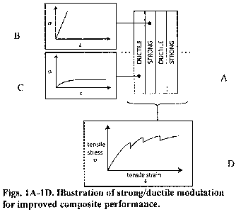
FIG. lA is an illustration of alternating strong layers and ductile layers to
form a composite.
FIG. 1B illustrates the stress versus strain curve for an individual strong
layer. FIG. 1C
illustrates the stress versus strain layer for an individual ductile layer.
FIG. 1D illustrates the
stress versus strain curve showing improved performance of the composite
(combination of
strong and ductile layers).
FIG. 2 is an illustration of a composite including grain modulation.
FIG. 3A is an illustration of a composite including modulated grain boundary
geometry. FIG.
3B is an illustration of another composite including modulated grain boundary
geometry.
FIG. 4 is an illustration of an NMC in accordance with the present disclosure
that includes layers
that alternate between two different preferred orientations.
FIG. 5 is an illustration of another NMC whose layers alternate between
preferred and random
orientations.
FIG. 6 is an illustration of another NMC whose layers possess alternating high
and low defect
densities.
FIG. 7 is an illustration of another NMC whose layers possess defects of
opposite sign. The
borders between the layers are darkened for clarity.
FIG. 8 is a graph of Vicker's micohardness versus plating bath temperature for
an iron (Fe)
material electrodeposited in accordance with the present disclosure.
CA 02730229 2011-01-07
WO 2010/005983 PCT/US2009/049832
-8-
FIG. 9 is a graph of ultimate tensile strength and percentage of elongation
versus frequency for
an electrodeposited Fe in accordance with the present disclosure.
FIG. 10 is an illustration of terminology that may be used to describe a sine
wave function used
to control the current density in the electrodepositionielectroformation
process. Positive values
of J (current density) are cathodic and reducing, whereas negative values are
anodic and
oxidizing. For net electrodeposition to take place with a sine wave function
the value of f3 must
be greater than one (i.e.. Joffset must be greater than one).
DETAILED DESCRIPTION
1. Modulation of Properties
In one embodiment, property modulated composites are provided comprising a
plurality of
alternating layers, in which those layers have specific mechanical properties,
such as, for
example, tensile strength, elongation, hardness, ductility, and impact
toughness, and where the
specific mechanical properties are achieved by altering the nanostructure of
those layers. This
embodiment is illustrated in Figs. 1A-1D.
In general, tensile strength may be controlled through controlling frequency
of a signal used for
electrodepositing a material. In general, percentage of elongation of a
material can also be
controlled through frequency. In general, hardness, ductility, and impact
toughness can be
controlled through controlling deposition temperature. Other methods for
controlling tensile
strength, elongation, hardness, ductility and impact toughness are also
envisioned.
Another embodiment provides property modulated composite comprising a
plurality of
alternating layers, in which those layers have specific thermal properties,
such as thermal
expansion, thermal conductivity, specific heat, etc. and where the specific
thermal properties are
achieved by altering the nanostructure of those layers.
2. Modulation of Structure
Another embodiment provides NMCs comprising a plurality of alternating layers
of at least two
nanostructures, in which one layer has substantially one grain size and
another layer has
substantially another grain size, and where the grain sizes may range from
smaller than 1
nanometer to larger than 10,000 nanometers. Such a structure is illustrated in
Fig. 2. Smaller
grain sizes, which can range, e.g., from about 0.5 nanometers to about 100
nanometers, generally
CA 02730229 2011-01-07
WO 2010/005983 PCT/US2009/049832
-9-
will yield layers that generally exhibit high impact toughness. Large grain
sizes, which generally
will be greater than 1,000 nanometers, such as, for example, 5,000 or 10,000
nanometers and
generally will produce layers that provide greater ductility. Of course, the
grain sizes will be
relative within a given group of layers such that even a grain size in the
intermediate or small
ranges described above could be deemed large compared to, e.g., a very small
grain size or small
compared to a very large grain size.
Generally, such grain sizes can be controlled through process parameters, such
as, for example
deposition temperature (e.g., electrodeposition bath temperature). To modulate
grain size
utilizing temperature control, a first layer defined by large grains can be
formed by increasing
the deposition temperature and a second layer defined by smaller grains can be
formed by
decreasing the temperature. (The material composition does not change between
the first and
second layers ¨ only the grain size modulates).
The thickness of the individual layers in the NMCs can range from about 0.1
nanometer to about
10,000 nanometers or more. Layer thickness may range from about 5 nanometers
to 50
nanometers, although varied thicknesses are expressly envisioned. The NMCs may
contain
anywhere from 2-10, 10-20, 20-30, 30-50, 75-100, 100-200, or even more layers,
with each layer
being created with a desired thickness, and nanostructure/microstructure.
When structural modulations are characterized by individual layer thicknesses
of 0.5 ¨ 5
nanometers, it is possible to produce materials possessing a dramatically
increased modulus of
elasticity, or "supermodulus." The modulated structural trait can include, for
example, one or
more of grain size, preferred orientation, crystal type, degree of order
(e.g., gamma-prime vs.
gamma), defect density, and defect orientation.
In another embodiment, NMCs can comprise a plurality of alternating layers of
at least two
nanostructures, in which one layer has substantially one inter-grain boundary
geometry and
another layer has substantially another inter-grain boundary geometry, as
illustrated in Figs. 3A
and 3B.
In still another embodiment, NMCs can comprise a plurality of alternating
layers of at least two
nanostructures, in which one layer has substantially one crystal orientation
and another layer has
substantially another crystal orientation (Fig. 4), or no preferred
orientation (Fig. 5).
CA 02730229 2011-01-07
WO 2010/005983 PCT/US2009/049832
-10-
In still another embodiment, NMCs can comprise a plurality of alternating
layers of at least two
nanostructures, in which one layer has grains possessing a substantially
higher defect density and
another layer has grains possessing a substantially lower defect density, an
example of which is
illustrated schematically in Fig. 6. Similarly, embodiments can include
materials whose layers
alternate between defect orientation or sign, as illustrated in Fig. 7.
In still another embodiment, NMCs or NGCs can comprise a plurality of
alternating layers or
diffuse zones of at least two nanostructures. Each layer or zone has a
mechanical, thermal,
and/or electrical property associated with it, which is a distinct property as
compared to an
adjacent layer or zone. For example, a NMC can include a plurality of first
layers each of which
have a Vicker's microhardness value of 400 and a plurality of second layers
each of which have
a Vicker's microhardness value of 200. The NMC is formed such that on a
substrate the first and
second layers alternate so that each of the deposited layers has a distinct
mechanical property as
compared to the layer's adjacent neighbor (i.e., the mechanical properties
across an interface
between first and second layers are different). In some embodiments, property
modulation in
Vicker's hardness is created by alternating the deposition temperature in an
electrochemical cell.
Referring to Fig. 8, the first layers having a Vicker's microhardness value of
400 can be formed
by electrodepositing Fe at a temperature 60 C, whereas second layers having a
Vicker's
microhardness value of 200 can be deposited at a temperature of 90 C.
In other embodiments, mechanical or thermal properties of NMCs or NGCs can be
controlled
through other deposition conditions such as, for example, frequency of an
electrical signal used
to electrodeposit layers on a substrate. In general, by increasing the
frequency of the signal
utilized in electrodeposition of a material, an increase in ductility (e.g.,
increase in ultimate
tensile strength and percentage elongation) can be realized as illustrated in
Fig. 9.
In addition to the frequency, the wave form of the electrical signal used to
electrodeposit layers
can also be controlled. For example, a sine wave, a square wave, a triangular
wave, sawtooth, or
any other shaped wave form can be used in electrodeposition. In general, the
frequency of the
waves can very from very low to very high, e.g., from about 0.01 to about
1,000 Hz, with ranges
typically being from about 1 to about 400 Hz (e.g., 10 Hz to 300 Hz, 15 Hz to
100 Hz). The
current also can be varied. Currents ranging from low to high values are
envisioned, e.g., from
CA 02730229 2011-01-07
WO 2010/005983 PCT/US2009/049832
-11-
about 1 to about 400 mA/cm2, with typical ranges being from about 10 to about
150 mA/cm2, in
particular, 20 to 100 mA/cm2.
3. Production Processes
One embodiment provides a process for the production of a property modulated
composite
comprising multiple layers with discrete nanostructures. This process
comprises the steps of:
i) providing a bath containing an electrodepositable species (i.e., a species
which when deposited
through electrodeposition forms a material, such as a metal);
ii) providing a substrate upon which the metal is to be electrodeposited;
iii) immersing said substrate in the bath;
iv) passing an electric current through the substrate so as to deposit the
metal onto the substrate;
and
v) heating and cooling the bath or the substrate according to an alternating
cycle of
predetermined durations between a first value which is known to produce one
grain size and a
second value known to produce a second grain size.
Another embodiment provides a process for the production of a property
modulated composite
comprising multiple layers with discrete nanostructures. This process
comprises the steps of:
i) providing a bath containing an electrodepositable species (e.g., a species
which forms a metal
when electrodeposited);
ii) providing a substrate upon which the metal is to be electrodeposited;
iii) immersing the substrate in the bath; and
iv) passing an electric current through the substrate in an alternating cycle
of predetermined
frequencies between a first frequency which is known to produce one
nanostructure and a second
frequency known to produce a second nanostructure.
Another embodiment provides a process for the production of a property
modulated composite
comprising multiple layers with discrete nanostructures. This process
comprises the steps of:
i) providing a bath containing an electrodepositable species (e.g., a species
which forms a metal
when electrodeposited);
ii) providing a substrate upon which the metal is to be electrodeposited;
iii) immersing the substrate in the bath;
iv) passing an electric current through the substrate in an alternating cycle
of predetermined
frequencies between a first frequency which is known to produce one
nanostructure and a second
CA 02730229 2011-01-07
WO 2010/005983 PCT/US2009/049832
-12-
frequency known to produce a second nanostructure, while at the same time
heating and cooling
the bath or the substrate according to an alternating cycle of predetermined
durations between a
first value and a second value.
Additional embodiments relate to processes for the production of a material
where production
parameters may be varied to produce variations in the material nanostructure,
including beta,
peak-to-peak current density, average current density, mass transfer rate, and
duty cycle, to name
a few.
In embodiments, the bath includes an electrodepositable species that forms an
iron coating/layer
or an iron alloy coating/layer. In other embodiments, the bath includes an
electrodepositable
species that forms a metal or metal alloy selected from the group consisting
of nickel, cobalt,
copper, zinc, manganese, platinum, palladium, hafnium, zirconium, chromium,
tin, tungsten,
molybdenum, phosphorous, barium, yttrium, lanthanum, rhodium, iridium, gold,
silver, and
combinations thereof.
Though the discussion and examples provided herein are directed to metallic
materials, it is
understood that the instant disclosure is equally applicable for metal oxides,
polymers,
intermetallics, and ceramics (all of which can be produced using deposition
techniques with or
without subsequent processing, such as thermal, radiation or mechanical
treatment).
EXAMPLES
The following examples are merely intended to illustrate the practice and
advantages of specific
embodiments of the present disclosure; in no event are they to be used to
restrict the scope of the
generic disclosure.
Example I: Temperature Modulation
One-dimensionally modulated (laminated) materials can be created by
controlled, time-varying
electrodeposition conditions, such as, for example, current/potential, mass
transfer/mixing, or
temperature, pressure, and, electrolyte composition. An example for producing
a laminated,
grain-size-modulated material is as follows:
1. Prepare an electrolyte consisting of 1.24M FeC12 in deionized water.
2. Adjust the pH of the electrolyte to -0.5-1.5 by addition of HC1.
CA 02730229 2011-01-07
WO 2010/005983 PCT/US2009/049832
-13-
3. Heat the bath to 95 C under continuous carbon filtration at a flow rate of
¨ 2-3 turns (bath
volumes) per minute.
4. Immerse a titanium cathode and low-carbon steel anode into the bath and
apply a current such
that the plating current on the cathode is at least 100 mA/cm2.
5. Raise and lower the temperature of the bath, between 95 C (large grains)
and 80 C (smaller
grains) at the desired frequency, depending on the desired wavelength of grain
size modulation.
Continue until the desired thickness is obtained.
6. Remove the substrate and deposit from the bath and immerse in deionized
(DI) water for 10
minutes.
7. Pry the substrate loose from the underlying titanium to yield a free-
standing, grain-size
modulated material.
Example II: Beta Modulation
This example involves electroplating NMCs by modulating the beta value. In
embodiments
where the current density is applied as a sine wave having (1) a peak cathodic
current density
value (J+>0), (2) a peak anodic current density value (k<0), and (3) a
positive DC offset current
density to shift the sine wave vertically to provide a net deposition of
material, properties of the
deposited layers or sections can be modulated by changing a beta value. (See
Fig. 10). The beta
value is defined as the ratio of the value of peak cathodic current density to
the absolute value of
peak anodic current density. At low beta value (< 1.3), the electroplated iron
layers have low
hardness and high ductility, while at high beta (> 1.5 ), the plated iron
layers have high hardness
and low ductility. The laminated structure with modulated hardness and
ductility makes the
material stronger than homogeneous material.
The electroplating system includes a tank, electrolyte of FeC12 bath with or
without CaC12,
computer controlled heater to maintain bath temperature, a power supply, and a
controlling
computer. The anode is low carbon steel sheet, and cathode is titanium plate
which will make it
easy for the deposit to be peeled off. Carbon steel can also be used as the
cathode if the deposit
does not need to be peeled off from the substrate. Polypropylene balls are
used to cover the bath
surface in order to reduce bath evaporation.
The process for producing an iron laminate is as follows:
1. Prepare a tank of electrolyte consisting of 2.0 M FeC12 or 1.7 M FeC12 plus
1.7 CaC12 in
deionized water.
CA 02730229 2011-01-07
WO 2010/005983 PCT/US2009/049832
-14-
2. Adjust the pH of the electrolyte to -0.5 ¨ 1.5 by addition of HC1.
3. Control the bath temperature at 60 C.
4. Clean the titanium substrate cathode and low carbon steel sheet anode with
deionized water
and immerse both of them into the bath.
5. To start electroplating a high ductility layer, turn on the power supply,
and controlling the
power supply to generate a shifted sine wave of beta 1.26, by setting the
following parameters:
250 Hz with a peak current cathodic current density of 43 mA/cm2 and a peak
anodic current
density of -34 mA/cm2 applied to the substrate (i.e., a peak to peak current
density of 78 mA/cm2
with a DC offset of 4.4 mA/cm2). Continue electroplating a for an amount of
time necessary to
achieve the desired high ductility layer thickness.
6. To continue electroplating a high hardness layer, change the power supply
wave form using
the computer, with a beta value of 1.6, by setting the following parameters:
250 Hz with a peak
current cathodic current density of 48 mA/cm2 and a peak anodic current
density of -30 mA/cm2
applied to the substrate (i.e., a peak to peak current density of 78 mA/cm2
with a DC offset of 9.0
mA/cm2). Continue electroplating for an amount of time needed to achieve the
desired high
hardness layer thickness. (Optionally, the temperature can be decreased to 30
C during this
deposition step to further tailor the hardness of the layer.)
7. Remove the substrate and deposit from the bath and immerse in DI water for
10 minutes and
blow it dry with compressed air.
8. Peel the deposit from the underlying titanium substrate to yield a free-
standing temperature
modulated laminate.
Example III: Frequency Modulation
This example describes a process of electroplating NMCs by modulating the
frequency of the
wave-form-generating power supply. The wave-form can have any shape, including
but not
limited to: sine, square, and triangular. At low frequency (< 1 Hz), the
plated iron layers have
high hardness and low ductility, while at high frequency (> 100 Hz), the
electroplated iron layers
have low hardness and high ductility. The laminated structure with modulated
hardness and
ductility makes the material stronger than homogeneous material.
The electroplating system includes a tank, electrolyte of FeC12 bath with or
without CaC12,
computer controlled heater to maintain bath temperature at 60 C, a power
supply that can
generate wave forms of sine wave and square wave with DC offset, and a
controlling computer.
The anode is a low carbon steel sheet, and the cathode is a titanium plate
which will make it easy
CA 02730229 2011-01-07
WO 2010/005983 PCT/US2009/049832
-15-
for the deposit to be peeled off Carbon steel can also be used as the cathode
if the deposit does
not need to be peeled off from the substrate. Polypropylene balls are used to
cover the bath
surface in order to reduce bath evaporation.
The process for producing an iron laminate is as follows:
1. Prepare a tank of electrolyte consisting of 2.0 M FeC12 or 1.7 M FeC12 plus
1.7 CaC12 in
deionized water.
2. Adjust the pH of the electrolyte to -0.5 ¨ 1.5 by addition of HC1.
3. Control the bath temperature at 60 C.
4. Clean the titanium substrate cathode and low carbon steel sheet anode with
deionized water
and immerse both of them into the bath.
5. To start electroplating a high ductility layer, turn on the power supply,
and controlling the
power supply to generate a sine wave having a beta of 1.26, by setting the
following parameters:
10-1000 Hz with a peak current cathodic current density of 43 mA/cm2 and a
peak anodic
current density of -34 mA/cm2 applied to the substrate (i.e., a peak to peak
current density of 78
mA/cm2 with a DC offset of 4.4 mA/cm2). Continue electroplating for an amount
of time
necessary to achieve the desired high ductility layer thickness.
6. To continue electroplating a high hardness layer, change the power supply
wave form (shifted
sine wave having a beta of 1.26) using the computer, with the following
parameters: 1 Hz with a
peak current cathodic current density of 43 mA/cm2 and a peak anodic current
density of -34
mA/cm2 applied to the substrate (i.e., a peak to peak current density of 78
mA/cm2 with a DC
offset of 4.4 mA/cm2). Keep on electroplating for a specific amount of time
which is determined
by the desired high hardness layer thickness.
7. Remove the substrate and deposit from the bath and immerse in deionized
(DI) water for 10
minutes and blow it dry with compressed air.
8. Peel the deposit from the underlying titanium substrate to yield a free-
standing temperature
modulated laminate.
Possible Substrates
In the examples described above the substrates used are in the form of a
solid, conductive
mandrel (i.e., titanium or stainless steel). While the substrate may comprise
a solid, conductive
material, other substrates are also possible. For example, instead of being
solid, the substrate
may be formed of a porous material, such as a consolidated porous substrate,
such as a foam, a
mesh, or a fabric. Alternatively, the substrate can be formed of a
unconsolidated material, such
CA 02730229 2011-01-07
WO 2010/005983 PCT/US2009/049832
-16-
as, a bed of particles, or a plurality of unconnected fibers. In some
embodiments, the substrate is
formed from a conductive material or a non-conductive material which is made
conductive by
metallizing. In other embodiments, the substrate may be a semi-conductive
material, such as a
silicon wafer The substrate may be left in place after deposition of the NMCs
or NGCs or may
be removed.
Articles Utilizing NMCs or NGCs
Layered materials described herein can provide tailored material properties,
which are
advantageous in advance material applications. For example, the NMCs and NGCs
described
herein can be used in ballistic applications (e.g., body armor panels or tank
panels), vehicle
(auto, water, air) applications (e.g., car door panels, chassis components,
and boat, plane and
helicopter body parts) to provide a bulk material that is both light weight
and structurally sound.
In addition, NMCs and NGC can be used in sporting equipment applications
(e.g., tennis racket
frames, shafts), building applications (support beams, framing),
transportation applications (e.g.,
transportation containers) and high temperature applications (e.g., engine and
exhaust parts).