Note: Descriptions are shown in the official language in which they were submitted.
CA 02731251 2016-05-18
PHYSICAL PROPERTY SENSOR WITH ACTIVE ELECTRONIC CIRCUIT AND
WIRELESS POWER AND DATA TRANSMISSION
SUMMARY
[0001] In various aspects, the wireless sensor s described herein are
configured to
record and transmit data as well as sense and, optionally, actuate to monitor
physical
properties of an environment and, optionally, effect changes within that
environment. In one
aspect, the implantable wireless sensor can comprise a power harvesting unit;
a voltage
regulation unit, a transducing oscillator unit, and a transmitting coil. The
voltage regulation
unit is electrically coupled to the power harvesting unit and is configured to
actuate at a
minimum voltage level. The transducing oscillator unit is electrically coupled
to the voltage
regulation unit and is configured to convert a sensed physical property into
an electrical
signal. Also, the transmitting coil is configured to receive the electrical
signal and to transmit
the electrical signal to an external antenna.
[0002] Optionally, the wireless sensor can be configured to delay the
energizing the
voltage regulation unit until a predetermined time delay has elapsed In one
example, a
resistive-capacitive (RC) circuit can be used to effect the desired delay.
100031 In a further aspect, the power harvesting unit can comprise an
antenna
configured to receive the external energizing magnetic field; a first
capacitor coupled to the
antenna that is configured to store energy in the resonance mode; and a means
for rectifying
and at least doubling voltage to be stored in a second capacitor for use by
the sensor at a
subsequent time.
FIGURES
[0004] The accompanying drawings, which are incorporated in and constitute
a part
of this specification, illustrate certain aspects of the instant invention and
together with the
description, serve to explain, without limitation, the principles of the
invention. Like
reference characters used therein indicate like parts throughout the several
drawings.
CA 02731251 2011-01-19
WO 2010/011612
PCT/US2009/051177
[0005] Figure 1 is a schematic circuit diagram showing one embodiment of
a power
harvesting unit that employs a voltage doubling scheme.
[0006] Figure 2 is a schematic circuit diagram showing one embodiment of
a circuit
comprising a power harvesting unit and an end of burst detection unit.
[0007] Figure 3 is a schematic circuit diagram illustrating one
embodiment of a
circuit having a voltage regulation circuit.
[0008] Figure 4 is a schematic circuit diagram showing one embodiment of
a circuit
schematic for the RC time-based oscillator unit.
[0009] Figure 5 is a schematic circuit diagram showing a variable
capacitor and an IC
that is configured to convert capacitance to a digital signal are utilized to
form a digital sensor
with a transducing capacitor.
[0010] Figure 6 is a schematic circuit diagram showing an MCU controlling
the
timing of the rest of the circuit. In addition, the MCU can provide the
control signal for the
transducing A-to-D converting unit, can store the measured data into local
memory, and can
deliver modulated data for transmission to the interrogator.
[0011] Figures 7(a) and 7(b) illustrate one embodiment of a PCB-based
sensor circuit
encapsulated by a fused silica housing.
[0012] Figure 8 is a schematic circuit diagram of an exemplary embodiment
of a
wireless sensor showing a coil (L1) that is an energy harvesting coil and a
capacitor (C10) or
a resistor (R5) that varies predictably with the measured physical property.
In one aspect, a
coil (L2) serves as a transmitting coil and a resistor (R1) acts as an
attenuator.
[0013] Figure 9 depicts a schematic circuit diagram for an exemplary
embodiment of
a wireless sensor that uses one coil instead of two.
[0014] Figure 10 depicts the same exemplary circuit as in Figure 9 but
with a voltage
doubling scheme.
[0015] Figure 11 is a schematic illustration of an exemplary experimental
set-up used
in one pressure sensing experiment.
[0016] Figure 12 is a graph showing the results of the pressure sensing
experiment
schematically shown in Figure 11.
2
CA 02731251 2011-01-19
WO 2010/011612
PCT/US2009/051177
DETAILED DISCRIPTION OF THE DESCRIPTION
[0017] The present invention can be understood more readily by reference
to the
following detailed description, examples, drawing, and claims, and their
previous and
following description. However, before the present devices, systems, and/or
methods are
disclosed and described, it is to be understood that this invention is not
limited to the specific
devices, systems, and/or methods disclosed unless otherwise specified, as such
can, of course,
vary. It is also to be understood that the terminology used herein is for the
purpose of
describing particular aspects only and is not intended to be limiting.
[0018] The following description of the invention is provided as an
enabling teaching
of the invention in its best, currently known embodiment. To this end, those
skilled in the
relevant art will recognize and appreciate that many changes can be made to
the various
aspects of the invention described herein, while still obtaining the
beneficial results of the
present invention. It will also be apparent that some of the desired benefits
of the present
invention can be obtained by selecting some of the features of the present
invention without
utilizing other features. Accordingly, those who work in the art will
recognize that many
modifications and adaptations to the present invention are possible and can
even be desirable
in certain circumstances and are a part of the present invention. Thus, the
following
description is provided as illustrative of the principles of the present
invention and not in
limitation thereof.
[0019] As used throughout, the singular forms "a," "an" and "the" include
plural
referents unless the context clearly dictates otherwise. Thus, for example,
reference to "a
capacitor" can include two or more such capacitors unless the context
indicates otherwise.
[0020] Ranges can be expressed herein as from "about" one particular
value, and/or to
"about" another particular value. When such a range is expressed, another
aspect includes
from the one particular value and/or to the other particular value. Similarly,
when values are
expressed as approximations, by use of the antecedent "about," it will be
understood that the
particular value forms another aspect. It will be further understood that the
endpoints of each
of the ranges are significant both in relation to the other endpoint, and
independently of the
other endpoint.
3
CA 02731251 2011-01-19
WO 2010/011612
PCT/US2009/051177
[0021] As used herein, the terms "optional" or "optionally" mean that the
subsequently described event or circumstance may or may not occur, and that
the description
includes instances where said event or circumstance occurs and instances where
it does not.
[0022] The present invention comprises wireless physical property sensors
incorporating active circuitry and systems incorporating the same. Optionally,
the sensors
can be integrated with a hermetic, unitary package. Active circuitry
comprises, e.g.,
integrated circuits (ICs). The inclusion of active circuitry in the electrical
design of a
wireless sensor imparts many new traits. It enables the sensor to sense
multiple physical
outputs of interest such as, but not limited to, temperature, flow, stress,
strain, and chemical
properties. The addition of active circuitry also decouples the parasitic
effects that would
otherwise present signal processing challenges, allows for precise
compensation or
calibration of the sensor and enables some level of real-time statistical
computing, averaging,
filtering or combination thereof to ensure the statistical fidelity of the
information collected
by the sensor. The active circuitry can be used to manage the power source¨be
it an on-
board temporary (e.g., a capacitor or ultra-capacitor) or a permanent (e.g., a
battery) source of
energy to operate the sensor in a partially or fully autonomous manner. The
active circuitry
allows for storage of multiple sets of information collected by the sensor or
used in
processing of the sensor data. Also, the active circuitry enables the storage
of personal
information relative to the identity of the host and/or the sensor.
Furthermore, the active
circuitry can enable the use of robust protocols and data transmission
techniques to
communicate with the interrogator, minimizing the risk of miscommunication and
simplifying the interrogator. Sensors ascending to the present invention find
widespread use
in biomedical, industrial, consumer and automotive applications.
[0023] Two distinct types of wireless sensors embodying the
characteristics of the
prior paragraphs are disclosed herein: analog and digital sensors. The terms
"analog" and
"digital" refer to the format of communication between the sensor and the
interrogator. The
analog sensor generates a variable frequency signal whose frequency precisely
represents the
data to be retrieved. The digital sensor digitizes information collected by
the sensor prior to
transmitting it to the interrogator using some type of binary modulation such
as, without
limitation, PSK, ASK and FSK.
4
CA 02731251 2011-01-19
WO 2010/011612 PCT/US2009/051177
Analog wireless sensor
[0024] In one aspect, the analog wireless sensor is comprised of the
following
components: a power harvesting unit, an "end of burst" detection unit, a
voltage regulation
unit, a transducing oscillator unit, and a transmitting coil. Each of these
components, as well
as their overall assembly and packaging, are exemplarily described below.
[0025] The power harvesting unit is comprised of an inductor (L) and a
capacitor (C).
The inductor couples RF magnetic fields and the capacitor forms a resonant
circuit when
connected with the inductor and rectifying diodes, energy storage capacitors,
and over-
voltage protection units. The L and C are tuned to the RF magnetic field
present with the
following equation for maximum energy harvesting.
Equation (1) f = (2 * * (LCP)-1
[0026] The number of rectifying diodes used varies according to the
geometry of the
circuit. At least one rectifying diode for half wave rectification and a
plurality of rectifying
diodes for full wave rectification are needed. In one non-limiting example, a
minimum of
one rectifying diode for half wave rectification and four rectifying diodes
for full wave
rectification can be used. Optionally, when higher voltage generation is
required, a voltage
multiplying scheme can be employed, such implementation can involve the
addition of a
number of diodes and capacitors. The energy storage capacitor employs
relatively large
capacitance value compared to other capacitors in the circuit because it is
the only energy
source for operation of the wireless sensor in sequential systems. The value
can vary from
hundreds of pico Farad to tens of microFarad. A Zener diode can be used as an
over-voltage
protection unit.
[0027] Figure 1 shows one embodiment of a power harvesting unit that
employs a
voltage doubling scheme. When the interrogator an generates energizing
magnetic field in
proximity to the sensor, the small antenna (Lr) and a capacitor (Cr) pick up
the AC voltage in
resonance mode. That AC voltage is rectified and charged to a first capacitor
C2 through
diode Dl. Again, the voltage charged in C2 is added to the AC voltage in Lr
and Cr, and
rectified and charged to capacitor Cs through diode D2. Now due to C2, D1, and
D2, the AC
voltage available in Lr and Cr is doubled and stored to a second capacitor,
Cs, as a DC
voltage to be used for sensor operation at a subsequent time. A zener diode
(Dz) may be
CA 02731251 2011-01-19
WO 2010/011612
PCT/US2009/051177
incorporated to provide over-voltage protection. This circuit is useful, when
the sensor chip
used requires high voltage.
[0028] In one aspect, in order to recognize the end of the RF magnetic
burst around
the sensor, a simple resistive-capacitive (RC) circuit can be used. The
capacitor of the RC
circuit remains charged while RF field is present. As soon as RF field is
removed, the
capacitor of the RC circuit discharges through the resistor of the RC circuit
with a
predetermined time delay. In one aspect, the time delay is programmed such
that energizing
RF magnetic field has decayed to a given threshold level. When the RC circuit
has
discharged, the rest of the circuit "wakes up" for data transmission¨i.e., the
discharge of the
capacitor triggers a switch to connect the rest of the circuit to the energy
storage capacitor.
Thus, the potential problem of interference of the RF field is avoided and the
sensor is able to
take advantage of the maximum time available for communication.
[0029] Figure 2 depicts one embodiment of a circuit comprising a power
harvesting
unit and an end of burst detection unit. When the interrogator generates an
energizing
magnetic field in proximity to the sensor, the electrical energy (i.e.,
voltage) is harvested and
stored to capacitor C2. During this energy harvesting time, transistor switch
QP is open, so
that the energy being stored is not available to the main sensor circuit and
is thus preserved.
The main sensor circuit will be connected to the #3 node of switch QP later.
As soon as the
energizing magnetic field disappears, switch QP closes (the #2 and #3 nodes of
QP are
electrically connected), and the voltage in C2 is available to power the
sensor.
[0030] The detailed explanation of the circuit depicted in Figure 2 is as
follows: The
Li and C3 pick up the AC voltage which is doubled and rectified to C2 through
C6 and two
diodes in BAS4OBRW (#1 and #5 node in BAS4OBRW). Simultaneously, the AC
voltage in
Li and C3 is doubled and rectified to C11 through C7 and two diodes in
BAS4OBRW (#2
and #4 node in BAS4OBRW). Due to the voltage in C11, the switch QP is open and
the
energy in C3 is not available to the #3 node of switch QP. When the energizing
field from
the interrogator is off, the voltage in C11 dissipates through resistor R and
becomes zero in
short time (i.e., less than a millisecond). As soon as the voltage in C11
becomes zero, the
switch QP closes and the voltage in C2 is available to main sensor circuit.
6
CA 02731251 2011-01-19
WO 2010/011612
PCT/US2009/051177
[0031] Thus, in one exemplary embodiment, the power harvesting unit is a
LC-tank
that is followed by a rectification stage and an optional voltage
multiplication stage. It is then
a energy storage stage, such as a capacitor with a desired energy storage
space.
[0032] Most of electronic oscillators call for precise control of supply
voltage for
accurate operation. This is true for the RC oscillator used in this scheme.
Because the
voltage source in the analog wireless sensor is a capacitor, the supply
voltages decay unless
the capacitance value is impractically large. A linear voltage regulator and a
voltage
reference can be used for its preciseness and simplicity. Since the linear
voltage regulator
and the voltage reference do not control voltage below their rated voltage, an
under-voltage
lockout is employed to avoid uncontrolled operation under the rated voltage of
the linear
voltage regulator and voltage reference by turning off the subsequent circuit
when the voltage
drops below the predetermined value.
[0033] Figure 3 illustrates one embodiment of a circuit having a voltage
regulation
circuit. The unit V1 is a voltage reference and U2 is an under-voltage lockout
unit. C8 is
noise reduction capacitor. The #1 node of V1 is connected to #3 node of QP
switch,
therefore the voltage stored in C2 is available to the #1 node of Vi. V1
functions to output a
preset voltage level whenever the input (#1) voltage is higher than preset
output voltage.
This ensures the voltage available to sensor transducer unit is substantially
constant The
sensor transducer unit is connected to output (#2) of Vi. The constant level
of voltage
contributes to the accurate functioning of the transducer unit. However, if
the input voltage
(#1 node) of V1 is lower than preset output voltage (#2 node), the output
voltage of V1
follows the input regardless of the preset output. This voltage variation can
add noise to
sensor transducer function when it is supplied to transducer unit. In order to
manage this
low-voltage faulty condition, U2 is employed. U2 monitors voltage in C8 and,
if the voltage
in C8 is smaller than preset voltage, it generates a warning or disabling
signal through #6
node of U2. The preset voltage level is adjusted with resistor values in R2,
R4, and R6.
When the voltage is higher than the preset voltage, then the preset voltage is
available to #6
node of U2. When the voltage in C8 is lower than the preset voltage, the zero
voltage is
available to #6 node of U2, either warning or disabling transducer unit.
[0034] Next, the transducing oscillator unit converts physical properties
such as, but
not limited to, pressure, temperature, stress and the like to electrical
signals. Subsequently,
the electrical signals set the electrical oscillation frequency, which is
transmitted to the
7
CA 02731251 2011-01-19
WO 2010/011612 PCT/US2009/051177
interrogator. This electrical frequency can be measured and correlated to the
value of the
measured physical property by the interrogator.
[0035] The RC time constant-based oscillator can be used for setting the
electrical
oscillation frequency. One example is a 555 timer. In one aspect, the
relationship between
frequency and the sensed property is described with the equation below:
Equation (2) f =(kRC )1,
where k is a proportional constant varying by design and operation frequency,
R and C are,
respectively, the resistor and capacitor values that sense the physical
property of interest. It is
contemplated that either one of the R or C values can be held constant and the
other can be
used to sense the physical property of interest.
[0036] Figure 4 shows one embodiment of a circuit schematic for the RC
time-based
oscillator unit. In this exemplary aspect, a capacitor (C10) or a resistor
(R5) represents the
sensing capacitor or sensing resistor. The #4 node is an operating-voltage
supply line, and #3
node is a chip-function enabling line. In this aspect, if zero voltage is
supplied to #3 node,
the whole chip is configured to shut down. In a further aspect, the line that
is in
communication with the #3 node can also be electrically coupled to the #6 node
of U2 in the
Figure 3, which acts to shut down the chip when the voltage is lower than the
preset voltage.
In one aspect, the exemplary circuit is configured such that the oscillator
frequency can be
varied by the value of C10 and R5 and can be available through the #5 node in
order to be
transmitted back to the reader or interrogator wirelessly.
[0037] Conventionally, a passive (no battery) LC resonant circuit is
composed of two
electrical passive components that are connected in series: a coil or inductor
("L"), and a
capacitor ("C"). Such a passive electrical circuit exhibits electrical
resonance when subjected
to an alternating electromagnetic field. In one aspect, the electrical
resonance is particularly
acute for a specific frequency value or range of the impinging signal. When
the impinging
signal substantially reaches the resonant frequency of the LC resonant circuit
inside the
sensor assembly, a pronounced disturbance of the field can be detected
wirelessly. In the
simplest approximation, the electrical resonance occurs for a frequency f,
related to the value
of L and C according to equation 1 above.
[0038] The passive electrical resonant circuit for the assemblies
described herein that
utilize a passive electrical resonant circuit can be fabricated via
conventional MEMS
8
CA 02731251 2011-01-19
WO 2010/011612
PCT/US2009/051177
approach to sensor design, which lends itself to the fabrication of small
sensors that can be
formed using biocompatible polymers as substrate materials. In a further
aspect,
appropriately biocompatible coatings can be applied to the surfaces of the
respective
assemblies in order to prevent adhesion of biological substances to the
respective assemblies
that could interfere with their proper function.
[0039] In one example, it is contemplated that the passive electrical
resonant circuit
of the assembly can be manufactured using Micro-machining techniques that were
developed
for the integrated circuit industry. An example of this type of sensor
features an inductive-
capacitive (LC) resonant circuit with a variable capacitor is described in
Allen et al., U.S. Pat.
No. 6,111,520, which is incorporated herein by reference. In this sensor, the
capacitance
varies with the pressure of the environment in which the capacitor is placed.
Consequently,
the resonant frequency of the exemplary LC circuit of the Allen pressure
sensor varies
depending on the pressure of the environment.
[0040] In one aspect, to convert stress to resistance, piezoresistive
material can be
used to transduce sensed stress to resistance. An example of this type of
sensor is
exemplarily described in Gershenfeld et al., U.S. Pat. No. 6,025,725, which is
incorporated
herein by reference.
[0041] In one aspect, to convert temperature to resistance, a thermistor
can be
employed. In this aspect, the thermistor is defined as a metal whose specific
electrical
resistance varies according to the temperature of a material. The
environmental temperature
determines the resistance which, in turn, determines the oscillation frequency
of the RC
oscillator unit. In this aspect, the thermistor is attached to the sensor
housing for better
thermal conduction.
[0042] Thus, it is contemplated that the sensor can be configured to
convert a sensed
physical property into an electrical signal comprises. For example and without
limitation,
this conversion can comprise converting sensed temperature changes to
resistance changes
via a temperature sensitive resistor. Further, for example and without
limitation, this
conversion can comprise converting sensed changes in pressure to changes in
capacitance
values via a pressure sensitive capacitor. In another example, for example and
without
limitation, this conversion can comprise converting sensed stress changes to
resistance
changes via a stress sensitive resistor.
9
CA 02731251 2011-01-19
WO 2010/011612
PCT/US2009/051177
[0043] Optionally, a voltage controlled oscillator (VCO) can also be used
for
transducing a physical property of interest to an electrical signal. A
conventional VCO is an
electronic circuit whose electrical oscillation output is a function of the
voltage applied. In
this aspect, the measured physical property is converted to a voltage that
determines the
broadcasting electrical frequency. Many physical properties are readily
converted to voltage.
For example, and without limitation, such convertible physical properties
include measured
temperature, stress, pressure or the like.
[0044] In one exemplary aspect, to accomplish a temperature to voltage
transduction,
a constant current source can be applied to a resistor. Here, the induced
voltage at the end of
the resistor is proportional to the value of the resistor. Therefore,
temperature change can be
converted to voltage through a thermistor.
[0045] In an additional exemplary aspect, to accomplish a stress or
pressure to
voltage transduction, four piezoresitors can be arranged into a Wheatstone
bridge
configuration, which is configured to achieve a higher voltage sensitivity
while geometrically
compensating for temperature effects. In this aspect, the stress applied by
the external
environment to the deformable region of the sensor determines the output
voltage of the
Wheatstone bridge, and which sets the electrical oscillation for broadcasting.
[0046] Optionally, it is contemplated that an identification signal or
signature can be
added to the transmitted signal. In order to attach such a signature, the
oscillation frequency
can be amplitude modulated prior to transmission to the interrogator.
Subsequently, the
interrogator can confirm this signature and authenticate that the frequency is
coming from a
specific wireless sensor or merely the wireless sensor at all. This signature
modality allows
for sensor identification and avoids any confusion with other resonances
present in the
environment.
Digital wireless sensor
[0047] In one aspect, a digital wireless sensor is comprised of the
following
components: a power harvesting unit, an end of burst detection unit, a
microcontroller unit
(MCU), a transducing analog-to-digital converter unit, and a transmitting
coil. Optionally, a
voltage regulation unit can be incorporated into the digital wireless sensor.
The design of the
power harvesting unit, the end of burst detection unit and the voltage
regulation unit are
substantially the same for the digital sensor as described above for the
analog sensor.
CA 02731251 2011-01-19
WO 2010/011612
PCT/US2009/051177
[0048] As shown in Figure 5, a variable capacitor and an IC that is
configured to
convert capacitance to a digital signal are utilized to form a digital sensor
with a transducing
capacitor. In operation, as indicated in Figure 6, the MCU sends out a signal
to start the
frequency generator and the counter. Substantially simultaneously, the
capacitance is
charged at a controlled rate. In one non-limiting example, a constant current
source or a
constant voltage source can be used to charge the capacitor. One skilled in
the art will
appreciate that the constant current source does not require a resistor can
also produce a more
linear digital output over a wide range of capacitance.
[0049] When the voltage of the capacitor reaches the reference voltage of
the voltage
regulator, the comparator trips and the counter is turned off. The MCU reads
the digital
output and discharges the capacitor in preparation for the next measurement.
In one aspect,
the digital output is a number that is substantially proportional to the
capacitance value. In a
further aspect, the digital output resolution depends on the frequency of the
frequency
generator, which should be kept high enough to support resolution of the
capacitance value
necessary for meaningful output to the end user of the system.
[0050] As schematically shown in Figure 6, the MCU controls the timing of
the rest
of the circuit. In addition, the MCU can provide the control signal for the
transducing A-to-D
converting unit, can store the measured data into local memory, and can
deliver modulated
data for transmission to the interrogator. Conventional off-the-shelf MCU
chips typically
comprise a frequency generator, a counter, and a comparator with voltage
references, and can
realize the schematic in Figure 6 with minimal components added.
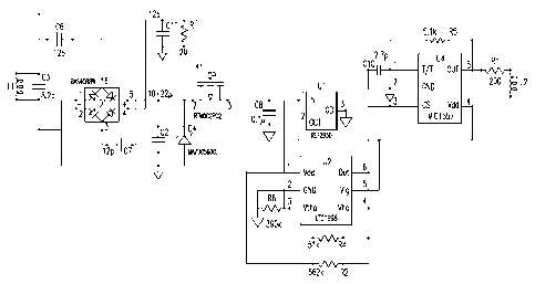
[0051] Figure 8 shows a schematic circuit diagram of an exemplary
embodiment of a
wireless sensor. As mentioned previously, a coil (L1) is an energy harvesting
coil and a
capacitor (C10) or a resistor (R5) varies predictably with the measured
physical property. In
one aspect a coil (L2) serves as a transmitting coil and a resistor (R1) acts
as an attenuator.
[0052] Figure 9 depicts a schematic for an exemplary embodiment of a
wireless
sensor that uses one coil instead of two. In one aspect the plurality of
inductor coils
employed in the previous examples are not functionally active simultaneously,
i.e., the
transmit coil is not in use while the energy pick up coil is active and vice-
versa. Therefore, a
single coil wireless sensor is achievable with certain modifications. In this
aspect, the output
of the transducer oscillator can be connected to the coil (L1) through MOSFET
switch M3
11
CA 02731251 2016-05-18
=
whenever the transducer oscillator activates and transmits a signal. Thus,
coil L1 can be used
for both energy harvesting and signal transmission. Figure 10 depicts the same
circuit as in
Figure 9 but with a voltage doubling scheme.
Packaging of wireless sensors
100531 In one aspect, the packaging of the sensors can
comprise encapsulating
PCB-based sensor circuits in ceramic housings. For example and without
limitation, the
ceramic housing can be completed either via laser fusion, anodic bonding or
eutectic
bonding. It is of course contemplated that the PCB-based sensor circuit can be
replaced with
an ASIC and this replacement is within the scope of the present invention. In
various
exemplary aspect, the sensor can be packaged by the methods disclosed in US
Patent
No. 7,574,792, tiled June 22, 2006.
In one
aspect, Figures 7(a) and 7(b) illustrate one possible embodiment of a PCB-
based sensor
circuit encapsulated by a fused silica housing.
100541 In one aspect, in operation, it is contemplated that the
external source of the
energizing magnetic field, such as an interrogator, will transmit energy at a
substantially
constant preselected frequency. In a further aspect, the external source will
activate or
energize for a predetermined period of time, during which time the power
harvesting unit of
the wireless sensor is energized. After the predetermined period of energizing
time has
passed, energy accumulated in the power harvesting unit is supplied to the
voltage regulation
unit and is subsequently supplied to the transducing oscillator unit at the
substantially
constant preset voltage level output from the voltage regulation unit.
Subsequently, the
electrical signal indicative of the sensed physical property is transmitted
via the transmitting
coil of the sensor to a remote, external antenna, which can form a portion of
the interrogator.
Experimental
100551 Figure 11 shows the brief illustration of an exemplary
experimental set-up
used in one pressure sensing experiment. In this experiment, the capacitor
(C10) in the
schematic illustrated in Figure 8 is replaced with a pressure sensitive
capacitor. Pressure was
applied to the sensor via a hand pump.
12
CA 02731251 2016-05-18
[0056] In this experiment, the timing control unit sent out periodic
triggering (on/off)
signal to RF power amp. A strong 13.56MHz signal was turned on/off at a rate
of 35Hz and
subsequently feed to the antenna. Here, whenever the 13.56MHz signal is turned
off, the
wireless pressure sensor "wakes up" and transmits the pressure information in
the form of
electrical frequency. A receiving antenna sensed the transmitted frequency by
wireless
sensor, and then the received signal was amplified and feed to the frequency
counter. The
results of the experiment are shown in Figure 12.
100571 The scope of the claims should not be limited by the preferred
embodiments set forth in the examples, but should be given the broadest
interpretation
consistent with the description as a whole.
=
=
13