Note: Descriptions are shown in the official language in which they were submitted.
CA 02731413 2011-01-19
WO 2010/009543 PCT/CA2009/001014
A MICROFLUIDIC DEVICE AND METHOD FOR FABRICATING THE
MICROFLUIDIC DEVICE
Related Applications
This application claims the benefit of U.S.
Provisional Patent Application No. 61/082,302 filed on
July 21, 2008, which is hereby incorporated by reference in its
entirety.
Field of the Invention
The invention relates to a microfluidic device for
use in excitation induced fluorescence testing.
Background of the Invention
The field of integrated Micro-Electro-Mechanical
Systems (MEMS) including microfluidics, microelectronics and
photonics offers a vast potential to realize low cost,
efficient and reliable means of sensing. This field has
recently attracted remarkable attention due to its potential of
implementing novel applications in numerous areas.
Investigation into the use of MEMS technology to produce
microdevices for biological applications, namely, Bio
MicroElectro Mechanical Systems (BioMEMS) has increased
recently in the hopes of developing opportunities and
commercializing devices in the areas of medicine, life
sciences, bio-security and Point-Of-Care (POC) diagnosis and
drug delivery.
Device portability is considered to be an important
feature for in-situ medical detection applications.
Miniaturization of a biosensor is also considered to be
important for ease of device handling, utilizing smaller sample
volumes and assisting in rapid or simple biological detection
leading to high throughput.
CA 02731413 2011-01-19
WO 2010/009543 PCT/CA2009/001014
2 -
In the past decade, BioMEMS applications in the area
of microfluidics have received enormous attention due to a) the
availability of suitable fabricating methodologies to make
individual and/or integrated devices, b) the quest for less
expensive and portable devices to perform simple and quick
analysis and c) the potential of micro-systems for use in
performing fundamental studies of physical, chemical and
biological processes in micro-level test samples. A majority
of work carried out on microfluidic devices has involved the
biomedical field, especially in the life sciences and
diagnostics domain - POC analysis, Micro Total Analysis Systems
(pTAS), DNA and proteomic chips, protein chips and cell chips.
Applications include separation of proteins and amino acids,
high throughput DNA analysis, cell culture and handling,
clinical diagnostics and immunoassays.
Summary of the Invention
According to an aspect of the present invention,
there is provided a polymer-based microfluidic device for
detecting induced fluorescence in a micro-volume of a fluid,
the device comprising: a top portion comprising: a wavelength
specific excitation source for inducing fluorescence in the
fluid; a lens for collecting emitted fluorescence from the
fluid; a bottom portion; a chamber having walls bounded by the
top portion and the bottom portion, the chamber configured to
contain the fluid, the chamber in fluid communication with at
least one inlet port for receiving the fluid and at least one
outlet port for removing the fluid; wherein an optical path of
emitted fluorescence from the chamber and an optical path of
light emitted by the excitation source do not share a common
path to the lens through the chamber.
In some embodiments, the device further comprises: a
filter located between the chamber and the lens, the filter for
reducing interference between the emitted fluorescence from the
fluid and other spectral components.
CA 02731413 2011-01-19
WO 2010/009543 PCT/CA2009/001014
3 -
In some embodiments, the device further comprises at
least one additional inlet port and at least one additional
outlet port for use in rinsing the chamber.
In some embodiments, the device further comprises a
detector for detecting light collected by the lens.
In some embodiments, the detector is a photodetector.
In some embodiments, the detector is a micro-
spectrometer.
In some embodiments, the micro-spectrometer comprises
a photodetector.
In some embodiments, an optical waveguide is located
between the lens and the micro-spectrometer.
In some embodiments, the optical waveguide is an
optical fiber.
In some embodiments, the micro-spectrometer is a
diffraction grating spectrometer.
In some embodiments, the lens is configured to couple
the emitted fluorescence from the fluid into an optical fiber.
In some embodiments, the optical fiber is attached to
the lens.
In some embodiments, the top portion includes at
least two layers, a first layer comprising the wavelength
specific excitation source and a second layer comprising the
lens and a detector, wherein the first layer is farther away
from the bottom portion than is the second layer.
In some embodiments, the device further comprises a
filter located between the chamber and the lens, the filter for
reducing interference between the emitted fluorescence from the
fluid and other spectral components.
CA 02731413 2011-01-19
WO 2010/009543 PCT/CA2009/001014
- 4 -
In some embodiments, the detector comprises a micro-
spectrometer and a photodetector.
In some embodiments, the micro-spectrometer is
monolithically integrated in the second layer.
According to another aspect of the present invention,
there is provided a polymer-based microfluidic device for
detecting induced fluorescence in a micro-volume of a fluid,
the device comprising: a top portion comprising: a wavelength
specific light excitation source for inducing fluorescence in
the fluid; a detector for detecting emitted fluorescence from
the fluid; a bottom portion; a chamber having walls bounded by
the top portion and the bottom portion, the chamber configured
to contain the fluid, the chamber in fluid communication with
at least one inlet port for receiving the fluid and at least
one outlet port for removing the fluid; wherein an optical path
of emitted fluorescence from the chamber and an optical path of
light emitted by the excitation source do not share a common
path to the detector through the chamber.
In some embodiments, the device further comprises a
filter located between the chamber and the detector, the filter
for reducing interference between the emitted fluorescence from
the fluid and other spectral components.
In some embodiments, the wavelength specific
excitation source is a narrow band source.
In some embodiments, the wavelength specific
excitation source is any one of: a wavelength specific light
emitting diode (LED); a wavelength specific organic LED (OLED)
and a semiconductor laser.
In some embodiments, the narrow band source is a blue
wavelength narrow band source.
CA 02731413 2011-01-19
WO 2010/009543 PCT/CA2009/001014
-
In some embodiments, the polymer-based device is
fabricated from one or more of the following:
polydimethylsiloxane (PDMS); photoresist, SU8; poly ethyl
acrylate (PEA); poly methyl methacrylate (PMMA); silicon doped
5 PDMS (PsiA); and other derivatives of these materials.
According to yet another aspect of the present
invention, there is provided a method for fabricating a
polymer-based microfluidic device for detecting induced
fluorescence in a micro-volume of a fluid, the method
comprising: forming a top portion comprising: integrating in a
polymer-based material a wavelength specific excitation source
and at least one of: a lens configured to collect fluorescence
emitted from the fluid; and a detector; forming a recess in a
surface of the top portion that is a partial boundary of a
chamber configured to contain the micro-volume of the fluid,
the chamber comprising at least one inlet port and at least one
outlet port; bonding the surface of the top portion to a bottom
portion, the bottom portion forming a remainder of the boundary
of the chamber.
In some embodiments, forming the top portion further
comprises: integrating a filter in the polymer-based material
for reducing interference between the fluorescence emitted from
the fluid and other spectral components.
In some embodiments, integrating in the polymer-based
material the wavelength specific excitation source comprises:
integrating one of: a wavelength specific light emitting diode
(LED); a wavelength specific organic LED (OLED) and a
semiconductor laser.
In some embodiments, forming the top layer comprises:
forming the top portion using a mould that forms the recess in
the surface of the top portion.
According to still another aspect of the present
invention, there is provided a method for fabricating a
CA 02731413 2011-01-19
WO 2010/009543 PCT/CA2009/001014
6 -
polymer-based microfluidic device for detecting induced
fluorescence in a micro-volume of a fluid, the method
comprising: forming a top portion comprising: integrating in a
polymer-based material a wavelength specific excitation source,
a lens for collecting emitted fluorescence from the fluid; a
detector; a waveguide between the lens and the detector;
forming a recess in a surface of the top portion that is a
partial boundary of a chamber configured to contain the micro-
volume of the fluid, the chamber comprising at least one inlet
port and at least one outlet port; bonding the surface of the
top portion to a bottom portion, the bottom portion forming a
remainder of the boundary of the chamber.
In some embodiments, forming the top portion further
comprises: integrating a filter in the polymer-based material
for reducing interference between the fluorescence emitted from
the fluid and other spectral components.
In some embodiments, forming the top portion
comprises forming the top portion in at least two layers, a
first layer comprising the wavelength specific excitation
source and a second layer comprising the lens and a detector,
wherein the first layer is farther away from the bottom portion
than is the second layer.
In some embodiments, integrating the detector
comprises integrating a micro-spectrometer and a photodetector.
In some embodiments, integrating the micro-
spectrometer comprises monolithically integrating a diffraction
grating spectrometer.
In some embodiments, forming the top layer comprises:
forming the top portion using a mould that forms the recess in
the surface of the top portion.
In some embodiments, integrating in the polymer-based
material the wavelength specific excitation source comprises:
CA 02731413 2011-01-19
WO 2010/009543 PCT/CA2009/001014
7 -
integrating one of: a wavelength specific light emitting diode
(LED); a wavelength specific organic LED (OLED) and a
semiconductor laser.
According to a further aspect of the present
invention, there is provided a microfluidic device for
detecting induced fluorescence in a micro-volume of a fluid,
the device comprising: a top portion comprising: a wavelength
specific excitation source for inducing fluorescence in the
fluid; a lens for collecting emitted fluorescence from the
fluid; a bottom portion; a chamber having walls bounded by the
top portion and the bottom portion, the chamber configured to
contain the fluid, the chamber in fluid communication with at
least one inlet port for receiving the fluid and at least one
outlet port for removing the fluid; wherein an optical path of
emitted fluorescence from the chamber and an optical path of
light emitted by the excitation source do not share a common
path to the lens through the chamber.
In some embodiments, the top portion is fabricated
from a polymer-based material and the bottom portion is
fabricated from a silicon-based material.
According to still a further aspect of the present
invention, there is provided a microfluidic device for
detecting induced fluorescence in a micro-volume of a fluid,
the device comprising: a top portion comprising: a wavelength
specific light excitation source for inducing fluorescence in
the fluid; a detector for detecting emitted fluorescence from
the fluid; a bottom portion; a chamber having walls bounded by
the top portion and the bottom portion, the chamber configured
to contain the fluid, the chamber in fluid communication with
at least one inlet port for receiving the fluid and at least
one outlet port for removing the fluid; wherein an optical path
of emitted fluorescence from the chamber and an optical path of
light emitted by the excitation source do not share a common
path to the detector through the chamber.
CA 02731413 2011-01-19
WO 2010/009543 PCT/CA2009/001014
8 -
In some embodiments, the top portion is fabricated
from a polymer-based material and the bottom portion is
fabricated from a silicon-based material.
According to another aspect of the present invention,
there is provided a method for fabricating a microfluidic
device for detecting induced fluorescence in a micro-volume of
a fluid, the method comprising: forming a top portion
comprising: integrating in a polymer-based material a
wavelength specific excitation source and at least one of: a
lens configured to collect fluorescence emitted from the fluid;
and a detector; forming a recess in a surface of the top
portion that is a partial boundary of a chamber configured to
contain the micro-volume of the fluid, the chamber comprising
at least one inlet port and at least one outlet port; bonding
the surface of the top portion to a bottom portion, the bottom
portion forming a remainder of the boundary of the chamber.
In some embodiments, bonding the surface of the top
portion to a bottom portion comprises bonding the surface of
the top portion to a bottom portion that is silicon based.
According to yet another aspect of the present
invention, there is provided a method for fabricating a
microfluidic device for detecting induced fluorescence in a
micro-volume of a fluid, the method comprising: forming a top
portion comprising: integrating in a polymer-based material a
wavelength specific excitation source, a lens for collecting
emitted fluorescence from the fluid; a detector; a waveguide
between the lens and the detector; forming a recess in a
surface of the top portion that is a partial boundary of a
chamber configured to contain the micro-volume of the fluid,
the chamber comprising at least one inlet port and at least one
outlet port; bonding the surface of the top portion to a bottom
portion, the bottom portion forming a remainder of the boundary
of the chamber.
CA 02731413 2011-01-19
WO 2010/009543 PCT/CA2009/001014
9 -
In some embodiments, bonding the surface of the top
portion to a bottom portion comprises bonding the surface of
the top portion to a bottom portion that is silicon based.
Other aspects and features of the present invention
will become apparent to those ordinarily skilled in the art
upon review of the following description of specific
embodiments of the invention in conjunction with the
accompanying figures.
Brief Description of the Drawings
Embodiments of the invention will now be described
with reference to the attached drawings in which:
Fig. 1 is a cross sectional view of a microfluidic
chip according to a first embodiment of the invention;
Fig. 2 is a cross sectional view of a microfluidic
chip according to a second embodiment of the invention;
Fig. 3 is a cross sectional view of a microfluidic
chip according to a third embodiment of the invention;
Fig. 4A is a cross sectional view of a microfluidic
chip according to a fourth embodiment of the invention;
Fig. 4B is a top view of a microfluidic chip shown in
Figure 4A;
Fig. 5A is a flow chart for a method of fabricating a
microfluidic chip according to an embodiment of the invention;
Fig. 5B is a flow chart for a method of fabricating a
microfluidic chip according to another embodiment of the
invention;
Fig. 6 is a cross sectional view of a master mould
template for fabricating a top portion of a microfluidic chip
according to an embodiment of the invention;
CA 02731413 2011-01-19
WO 2010/009543 PCT/CA2009/001014
- 10 -
Fig. 7 is a cross sectional view of the master mould
template of Figure 6 in which a polymer has been added to form
a first polymer layer;
Fig. 8 is a cross sectional view of the master mould
template of Figure 6 in which washers/o-rings are located at
positions of the ports and an LED is located within the top
portion;
Fig. 9 is a cross sectional view of a cured polymer
chip that is removed from the master template and forms a top
portion of the microfluidic chip;
Fig. 10 is a cross sectional view of the top portion
of the microfluidic chip with PVC tubes inserted;
Fig. 11 is a cross sectional view of the top portion
of a microfluidic chip attached with a bottom portion;
Fig. 12 is a cross sectional view of a microfluidic
chip according to a further embodiment of the invention
Fig. 13 is a schematic diagram of a bio-optical
fluorescence detection system using a microfluidic chip
according to an embodiment of the invention;
Figs. 14, 15, 17 and 18 are graphical plots showing
results from testing of a prototype microfluidic chip; and
Fig. 16 is a cross sectional view of a microfluidic
chip that indicates how residence time for inlet and rinsing
flows were calculated during testing of the prototype
microfluidic chip.
Detailed Description of the Embodiments of the Invention
The present application is directed to a
technological platform with integrated microfluidic and optical
modules for bio-detection.
CA 02731413 2011-01-19
WO 2010/009543 PCT/CA2009/001014
- 11 -
The platform enables in-situ detection by integrating
fluidics with optical source and detection capabilities within
a fabricated microchip. The platform is a polymer-based or
polymer and silicon based microfluidic chip having integrated
excitation source and detection elements in a vicinity of a
microfluidic reaction chamber configured to contain a micro-
volume of a test sample. The principle of detection is based
on a bio species, for example antigen, antibodies, cells,
enzymes, etc., which is tagged with a marker, such as a quantum
dot and/or nano particle that is capable of fluorescing. An
excitation source is used to induce fluorescence of the marker
within the microfluidic reaction chamber.
In some embodiments, the excitation source is a
wavelength specific light emitting diode (LED). LEDs are a
suitable excitation source as some types of LEDs have a
characteristic of generating a specific wavelength with high
luminous intensity at low drive voltages. Some LEDs also have
a divergence angle that can be advantageous in illuminating the
reaction chamber. For example, a suitable amount of excitation
light for a sample within a reaction chamber on the order of a
few mm2 can be provided by a wavelength specific LED having a
divergence angle of approximately 50 , in close proximity to
the reaction chamber.
Using a wavelength specific LED with a narrow
bandwidth reduces possible interference with the wavelength of
the emitted fluorescence signal from the reaction chamber.
This avoids the need for a sharp band pass filter to attenuate
light from the excitation source such as would be the case if a
broadband source was used as the excitation source. The
wavelength specific LED provides a stable excitation source
with increased sensitivity.
In some embodiments the excitation source is a narrow
band, blue wavelength source.
CA 02731413 2011-01-19
WO 2010/009543 PCT/CA2009/001014
- 12 -
While a wavelength specific LED is described as an
example of an excitation device, it is not intended to limit
the scope of the invention. In some embodiments, fluorescent
excitation is achieved using a laser source. For example, a
semiconductor laser device may be used due to the small size of
the device. In some embodiments, fluorescent excitation is
achieved using a xenon arc lamp. In some embodiments,
fluorescent excitation is achieved using an Organic Light
Emitting Diodes (OLED) source.
In some embodiments, the detection elements include
one or more of: a lens for collecting emitted fluorescence
wavelengths from the reaction chamber, a photodiode and a
micro-spectrometer. Examples of a detector using one or more
of the detection elements may include, but are not limited to,
a lens coupled to an optical fiber where the optical fiber is
connected to an external photodiode or spectrometer, a
photodiode in close proximity to the reaction chamber, with or
without a lens, or a micro-spectrometer including a
photodetector integrated in the chip, with or without a lens,
and an optical waveguide between the lens and micro-
spectrometer. In some embodiments, coupling optics may be used
to couple light from the reaction chamber into the waveguide
and/or the waveguide into the micro-spectrometer. In some
implementations the coupling optics include grin lenses.
The microfluidic chip may have an integrated filter
for filtering light from the excitation source before it
reaches the reaction chamber or a filter for filtering light
after it is emitted from the reaction chamber, but before it
reaches the detection elements to reduce spectra that may
interfere with the emitted light.
In some embodiments, the excitation wavelength
bandwidth of the excitation source is narrowed using an
excitation filter so as to provide a source excitation
wavelength within required parameters. In a particular
CA 02731413 2011-01-19
WO 2010/009543 PCT/CA2009/001014
- 13 -
implementation, a filter can be monolithically fabricated using
a polymer-based material at a location between the excitation
source and the reaction chamber to act as a narrow bandwidth
filter and allow only a desired wavelength or range of
wavelengths to reach the reaction chamber. In some
implementations, a discrete filter element of a material other
than a polymer-based material is embedded in the chip. In some
implementations a polymer-based material is used to
monolithically integrate a filter.
In some embodiments, a filter is embedded within the
microfluidic chip between the detection elements and the
reaction chamber to filter the excitation source wavelengths
and other external noise. In some implementations the filter
reduces interference with the wavelengths emitted from the
reaction chamber and increases sensitivity of the device. In a
particular implementation, a filter can be monolithically
fabricated using a polymer-based material at a location between
the detecting elements and the reaction chamber to act as a
narrow bandwidth filter and allow only a desired wavelength or
range of wavelengths to reach the detector. In some
implementations, a discrete filter element formed of a material
other than a polymer-based material is embedded in the chip.
The microfluidic chip may be fabricated using
multiple portions of a polymer-based material. A first portion
and a second portion are on opposite sides of the microfluidic
reaction chamber. For convention purposes, the first portion
will be referred to as a top portion and the second portion
will be referred to as a bottom portion. In some embodiments,
the reaction chamber and channels providing a path for the test
sample to reach the chamber may be formed in the top portion.
The bottom portion is then bonded to the top portion, forming
the reaction chamber for containing the test sample. In some
embodiments, the reaction chamber and channels providing a path
for the test sample to reach the chamber may be formed in the
bottom portion. The top portion is then bonded to the bottom
CA 02731413 2011-01-19
WO 2010/009543 PCT/CA2009/001014
- 14 -
portion, forming the reaction chamber for containing the test
sample. In some embodiments, the reaction chamber and channels
providing a path for the test sample to reach the chamber may
be formed partially in each of the top and bottom portions.
The portions are then bonded together, forming the reaction
chamber for containing the test sample.
In some embodiments, the top portion has embedded
within it the excitation source and detection elements for
detecting light emitted from within the reaction chamber. In
some embodiments, the top portion has embedded within it the
excitation source, and elements for detecting light emitted
from within the reaction chamber are bonded to a surface of the
top portion opposite to the bottom surface which is bonded to
the bottom portion. An example of an element for detection of
light is a lens.
In some embodiments, either of the top portion or the
bottom portion can be fabricated using a multi-layer process.
For example, the top portion may be formed using two layers.
In some implementations a first layer of the top portion may be
a functional layer, in which a lens, a micro-spectrometer and
an optical waveguide from the lens to the micro-spectrometer
are monolithically formed, and a photodetector is embedded. In
some implementations some or all of the lens, optical waveguide
and micro-spectrometer are discrete components embedded in the
functional layer. The functional layer is the layer located
closest to the bottom portion when the top and bottom portions
are bonded together. The excitation source is embedded in a
second layer of the top portion formed on top of the functional
layer.
In some embodiments, the excitation source and the
detection elements are located in the same portion, top or
bottom, and are on the same side of the reaction chamber. An
optical path of fluorescence emitted from within the reaction
chamber in the direction of the detection element and an
CA 02731413 2011-01-19
WO 2010/009543 PCT/CA2009/001014
- 15 -
optical path of light emitted by the excitation source in the
direction of the reaction chamber do not share a common path to
the detection element through the reaction chamber. In some
embodiments, since the optical path of fluorescence to the
detection element and the optical path of light emitted by the
excitation source to the reaction chamber do not share a common
path to the detection element through the reaction chamber, a
filter to attenuate light from the excitation source may not be
needed. The filter may not be needed as the amount of light
received by the detection elements is significantly less than
compared to a situation when the source and detector elements
are on opposite sides of the reactive chamber share a direct
path that includes the reaction chamber.
In some embodiments where a filter is used to reduce
interference between the source and light emitted from the
fluid in the reaction chamber, the filter can be physically
smaller in size than filters that are needed in a situation
where the source and detector elements have a direct path that
includes the reaction chamber. When the optical path of
fluorescence from the reaction chamber and the optical path of
light emitted by the excitation source that pass through the
reaction chamber do share a common path to the detection
elements through the reaction chamber, a filter needs to
attenuate a significantly higher intensity from the excitation
source since the light emitted by the excitation source is on
the same path as the light emitted by the fluid in the chamber.
In some embodiments, positioning of the excitation
source and detecting elements in the microfluidic chip can be
optimized so as to reduce the amount of light emitted from the
excitation source that is directly received by the detecting
elements.
When considering suitable material from which to
fabricate the microfluidic chip, several factors should be
considered. Some of the factors may include, but are not
CA 02731413 2011-01-19
WO 2010/009543 PCT/CA2009/001014
- 16 -
limited to, a) optical, electrical, thermal and mechanical
properties of the material, b) ease of working with the
material during fabrication, interconnection and packaging, c)
permeability of the material and d) biocompatibility of the
material with the testing species.
Polydimethylsiloxane (PDMS) is one of the
predominantly used materials in fabricating microfluidic
devices, especially for biomedical applications. The
commercial name of PDMS is Sylgard 184 (Dow Corning Corp.). In
some embodiments of the present invention, PDMS is used as a
microfluidic device substrate due to its ease of fabrication
and integration with excitation source and detection elements
to make a hybrid integrated device. Moreover, PDMS is
optically transparent in the near UV and visible ranges of the
electromagnetic spectrum. The material is both electrically
insulating and thermally insulating.
While PDMS is an example of a material that could be
used in the fabrication of the device it is not meant to limit
the type of materials that could be used. For example, other
materials that may be used for fabrication include, but are not
limited to, photoresist, SU8, poly ethyl acrylate (PEA), poly
methyl methacrylate (PMMA) and silicon doped PDMS (PsiA).
In some implementations, the microfluidic chip is a
polymer and silicon based platform. For example, in some
embodiments, the top portion is polymer-based and the bottom
portion is silicon based. Further examples of such
implementations will be described in greater detail below.
Design Implementations
A first example embodiment of a microfluidic chip
with an embedded wavelength specific LED source will now be
discussed with regard to Fig. 1.
CA 02731413 2011-01-19
WO 2010/009543 PCT/CA2009/001014
- 17 -
The microfluidic chip 100 consists of an inlet port
160A and at least one rinsing ports (not shown), which
intersect and lead to an outlet port 160B. In a particular
implementation, not intended to limit the invention, the inlet,
outlet 160A,160B and rinsing ports are 1 mm deep and are each
2 mm in diameter. The inlet, outlet 160A,160B and rinsing
ports are each in fluid connection with a respective channel
155 within the microfluidic chip 100. A region where the
channels 155 intersect is a reaction chamber 150. The reaction
chamber 150 is a volume within the microfluidic chip 100 that
contains a sample under test when the chip is in use. In some
embodiments, the reaction chamber 150 is also a center of
interest for enzyme interactions and optical detection. In
some implementations, the reaction chamber 150 is designed by
taking into account the micro-fluidic chip may be reusable.
For example, a shape is chosen that avoids corners, which may
be difficult to rinse between different samples.
Microfluidic chip 100 includes a top layer 110 and a
bottom layer 120. The bottom layer 120 forms a base for the
top layer 110. In some embodiments, the reaction chamber 150
is an empty volume between the top layer 110 and the bottom
layer 120. As illustrated in Fig. 1, inlet port 160A is an
ingress port to provide a test sample to the reaction chamber
150 and outlet port 160B is an egress port to allow the removal
of the sample. A wavelength specific LED source 130 is
embedded in the top layer 110 in close proximity to the
reaction chamber 150. Electrical connections 135 for LED 130
are exposed outside of the top layer 110. The electrical
connections 135 can be connected to a power supply to power LED
130. A lens 140 is bonded on a top surface of the top layer
110. An optical fiber 145 is coupled to the lens.
In operation, a sample in the form of a fluid
containing tagged markers is introduced via the inlet port 160A
into the channel 155 and fills the reaction chamber 150. In
some embodiments, the tagged markers may include one or more
CA 02731413 2011-01-19
WO 2010/009543 PCT/CA2009/001014
- 18 -
of, but not limited to, the following types of tagged markers:
fluorophores; quantum dots; dyes; and nano particles. Light
from the powered LED 130 excites the tagged markers of the
sample in the reaction chamber 150 and causes the markers to
fluoresce. The fluorescence emitted in a direction toward a
top surface of the top layer 110 is collected by the lens 140
and is coupled into the optical fiber 145. The optical fiber
145 is coupled to a measurement recording device to provide an
indication of the amount of fluorescence in the sample. In
some implementations, the measurement recording device may
include a spectrometer and/or other measurement recording
software/hardware and/or a display.
A second example embodiment of a microfluidic chip
with an embedded wavelength specific LED source, light
collecting lens and optical fiber will now be discussed with
regard to Fig. 2. Microfluidic chip 200 illustrated in Fig. 2
is similar to the microfluidic chip 100 of Fig. 1 in several
respects. Microfluidic chip 200 includes a top layer 110 and a
bottom layer 120. The reaction chamber 150 is located between
the top layer 110 and the bottom layer 120. Inlet and outlet
ports 160A,160B and channels 155 are passages through the top
layer 110 in fluid communication with the reaction chamber 150.
The wavelength specific LED source 130 is embedded in the top
layer 110 in close proximity to the reaction chamber 150.
With regard to detecting fluorescence emitted from
tagged markers of the sample in the reaction chamber 150, a
lens 220 and an optical fiber 225 are embedded in the top layer
110 in close proximity to the reaction chamber 150. In some
embodiments, a diverging lens is used to collect the emitted
fluorescence. In some embodiments, the lens and optical fiber
are discrete components that are coupled together during the
fabricating process. In other embodiments, the lens and
optical fiber are an integrated component before embedding the
component into the microfluidic chip 200.
CA 02731413 2011-01-19
WO 2010/009543 PCT/CA2009/001014
- 19 -
In the illustrated embodiment, a filter 210 is also
embedded in the top layer 110 between the reaction chamber 150
and the lens 220. The filter 210 is used to block wavelengths
of excitation signal from the LED 130 and scattered light that
may interfere with the fluorescence emitted from the reaction
chamber 150. While a filter may be advantageous in some
implementations, for example to improve the sensitivity of the
device, other implementations may not include such a filter.
Operation of the second embodiment is substantially
the same as the first embodiment.
In some implementations embedding the fiber 145 and
lens 220 within the microfluidic chip 200 may allow repetitive
sets of measurements to be achieved in a more consistent
manner.
A third example embodiment of a microfluidic chip
with an embedded wavelength specific LED source will now be
discussed with regard to Fig. 3. In the illustrated embodiment
of Fig. 3, several of the elements are substantially the same
as those in Figs. 1 and 2. For example, microfluidic chip 300
includes the top layer 110, the bottom layer 120, the
wavelength specific LED source 130, the reaction chamber 150,
and inlet, outlet 160A, 160B and rinsing ports. However, in
the example of Fig. 3, instead of using a lens and optical
fiber to collect fluorescence emitted from the microfluidic
chamber 150, a photodetector 320 is embedded in the top layer
110 in close proximity to the reaction chamber 150. The
photodetector 320 has electrical connections 325 extending out
of the top layer 110 to power the photodetector 320, if it is
an active component, and to provide the electrical signal
representing the received optical fluorescence to a measurement
recording device and/or a display.
In some other embodiments, there are optical
elements, such as, for example, a filter, and/or one or more
CA 02731413 2011-01-19
WO 2010/009543 PCT/CA2009/001014
- 20 -
lens between the detector and microfluidic chamber for
efficient light collection (not shown in Fig. 3).
The embodiment illustrated in Fig. 3 includes a high
transmission cut off filter 310 embedded in the top layer 110
between the reaction chamber 150 and the photodetector 320.
The filter 310 is used to block wavelengths of the excitation
signal and scattered light that may interfere with the output
signal. While the filter may be advantageous in some
implementations, for example to improve the sensitivity of the
device, other implementations may not include such a filter.
In some embodiments, the photodetector 320 is a
wavelength specific photodetector.
A photodetector integrated into the microfluidic chip
may make the microfluidic chip 300 simpler and easier to handle
as compared to the two previously described embodiments. Those
embodiments generate an optical signal that is converted to an
electrical signal external to the device. Any loses in the
optical signal along the path prior to the conversion to an
electrical signal may negatively affect the resulting
measurement. The present embodiment converts the optical
signal to an electrical signal substantially at the point of
measurement. In some embodiments, the embedded photodiode may
improve robustness and sensitivity of testing performed by the
microfluidic chip 300.
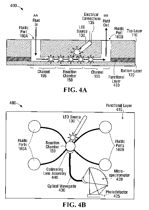
A fourth example embodiment of a microfluidic chip
with an embedded wavelength specific LED source will now be
discussed with regard to Fig. 4A and Fig. 4B. In the
illustrated embodiment of Fig. 4A and Fig. 4B, several of the
elements are substantially the same as those in Figs. 1 and 2.
For example, microfluidic chip 400 includes the top layer 110,
the bottom layer 120, the wavelength specific LED source 130,
the reaction chamber 150, and inlet, outlet 160A, 160B and
rinsing ports.
CA 02731413 2011-01-19
WO 2010/009543 PCT/CA2009/001014
- 21 -
Microfluidic chip 400 includes a third polymer layer,
a functional layer 410, located between the bottom layer 120
and top layer 110. In some implementations, the functional
layer 410 is substantially the same thickness as the reaction
chamber 150. However, in other implementations, the functional
layer 410 has a thickness that is greater than or less than the
reaction chamber 150. The functional layer 410 includes a
fabricated integrated micro-spectrometer 420, as indicated in
Fig. 4B. A collimating lens assembly 440 is located in the
functional layer 410 in close proximity to the reaction chamber
150 to collect fluorescence emitted by the test sample that is
illuminated in the reaction chamber. In some embodiments, the
collimating lens assembly 440 includes a filter to attenuate
spectral components that may interfere with the fluorescence
emitted from the sample. While a filter may be advantageous in
some implementations, for example to improve the sensitivity of
the device, other implementations may not include such a
filter.
An optical waveguide 430 is located between the
collimating lens assembly 440 and the micro-spectrometer 420.
In some embodiments the optical waveguide 430 is an optical
fiber embedded in the functional layer 410. In some
embodiments the optical waveguide 430 is a material with a
different index of refraction than the rest of the functional
layer 410. In some embodiments, the multiple layers of the
device could be different polymer materials having different
optical properties to achieve optical propagation in the
functional layer 410.
In some embodiments, a photodetector 425 is embedded
in the functional layer 410 in close proximity to the micro-
spectrometer 420 at a location allowing diffracted light from
the micro-spectrometer 420 to be detected. In some
embodiments, the fabrication of microfluidic chip 400 is
achieved by monolithically integrating micro-moulded gratings
and embedding a photodetector assembly in the functional layer
CA 02731413 2011-01-19
WO 2010/009543 PCT/CA2009/001014
- 22 -
410. In other embodiments, the photodetector is externally
attached.
In operation, the powered LED source 130 causes the
test sample in the reaction chamber 150 to fluoresce.
Fluorescence emitted from the reaction chamber 150 in the
direction of the collimating lens assembly 440 is collected by
the collimating lens assembly 440. The collimated light
propagates through the optical waveguide 430 to the micro-
spectrometer 420. The fluorescence light is diffracted by
gratings of the micro-spectrometer 420 and is detected by the
photodetector 425. The output of the photodetector 425 is
provided to a measurement recording device and/or a display.
In some implementations, functionality is
incorporated into the microfluidic chip to enable the channels
and reaction chamber to be rinsed out.
In some embodiments, size matching of reaction
chamber geometry with the detection elements provides improved
signal detection capability and sensitivity.
In some embodiments, circuits and electronic chips
for applications involving enzyme transduction, separation,
counting and imaging of flowing samples may be integrated into
the microfluidic chip.
In some embodiments, performance and functionality in
terms of measurement resolution, sensitivity and repeatability
is improved by an ability to incorporate the excitation source
and detection elements in close proximity within the
microfluidic chip.
In some embodiments, a minimum detectable limit of
fluorescence is improved due to the close proximity of the
excitation source and the detection elements with the reaction
chamber.
CA 02731413 2011-01-19
WO 2010/009543 PCT/CA2009/001014
- 23 -
In the embodiments described above, the channels and
reaction chamber are described as formed in the top layer, but
this is not intended to limit the device to this specific
implementation. In other implementations, the channels could
be formed in the bottom layer, or partially in the top layer
and partially in the bottom layer.
Fabrication of the Polymer-based Microfluidic Chip
Soft lithography has emerged as a popular fabrication
technique for microfluidic devices. It is a simple, effective
and inexpensive fabrication technique that uses a polymer in a
replica moulding type process. The technique does not need a
clean room facility for fabrication.
However, fabrication of the described microfluidic
chips is not intended to be limited to this process and other
processes are contemplated. Some other possible fabrication
methods may include, but are not limited to, Nanoimprint
lithography, embossing, bonding and lithography on polymers.
In some implementations of fabricating the top PDMS
layer, fabrication is based on two-layer soft lithography
technique. Such a process may be used in fabricating
microfluidic chips according to the first three example
embodiments described above. In some embodiments, a three-
layer soft lithography technique is used in fabrication. Such
a process may be used in fabricating microfluidic chips
according to the fourth example embodiment described above.
The two and three-layer soft lithography techniques allow
integrating of the LED source, excitation and/or emission
filters, if desired, and detection elements, such as lenses,
photodetectors and/or micro-spectrometers, within the
microfluidic chip.
With reference to Figs. 5A and 5B, general methods
for fabricating a microfluidic chip will now be described. The
fabrication methods include forming a top portion of the chip
CA 02731413 2011-01-19
WO 2010/009543 PCT/CA2009/001014
- 24 -
and bonding the top portion to a bottom portion. Forming the
top portion involves embedding discrete source components and
detection elements in a polymer-based material that forms the
top portion. The detection elements may be discrete components
and/or monolithically integrated in the polymer-based material.
The bottom surface of the top portion has recesses that, in
part, form channels and a reaction chamber. Once the bottom
portion is bonded to the top portion, the channel and reaction
chamber recesses form sealed conduits, accessible by inlet and
outlet ports, and a reservoir to receive a test sample.
In some implementations of fabricating the device, a
preliminary step involves forming a master template consisting
of a positive impression of a pattern used to create the top
portion of the microfluidic chip. The positive impression for
example forms the recesses of the channels and reaction chamber
in the bottom surface of the top layer. In some embodiments,
the master template is created using micromachining techniques
on silicon or other materials.
In Fig. 5A, fabricating the microfluidic chip
involves forming the top portion. Forming the top portion
involves several steps. A first step 5-1 of forming a top
portion involves integrating in a polymer-based material a
wavelength specific LED and at least one of a) a lens
configured to collect fluorescence emitted from the fluid and
b) a detector. In some embodiments, a filter for reducing
interference between the emitted fluorescence from the sample
and other spectral components may also be integrated in the top
portion. A second step 5-2 of forming a top portion involves
forming a recess in a surface of the top portion that is a
partial boundary of a chamber configured to contain a micro-
volume of the fluid that is the test sample, the chamber
comprising at least one inlet port and at least one outlet
port. The steps may be performed simultaneously, in the
sequence described, or in a reverse of the described sequence.
CA 02731413 2011-01-19
WO 2010/009543 PCT/CA2009/001014
- 25 -
A subsequent step 5-3 of fabricating the microfluidic
chip involves bonding the surface of the top portion to a
bottom portion, the bottom portion forming a remainder of the
boundary of the chamber.
In some embodiments, such a method of fabricating a
microfluidic chip may be used for fabricating chips similar to
the first, second and third microfluidic chip example
embodiments described above. A more detailed example of a
fabrication process will be described below.
In Fig. 5B, fabricating the microfluidic chip
involves forming a top portion of the device. Forming the top
portion involves several steps. A first step 5-10 of forming a
top portion involves integrating in a polymer-based material a
wavelength specific LED, a lens for collecting emitted
fluorescence from the fluid; a detector; and a waveguide
between the lens and the detector. In some embodiments, a
filter for reducing interference between the emitted
fluorescence from the sample and other spectral components may
also be integrated in the top portion. In some embodiments,
integrating the detector in the top portion involves
monolithically integrating a spectrometer in the top portion.
In some embodiments, components integrated in the top portion
are discrete components. A second step 5-11 of forming a top
portion involves forming a recess in a surface of the top
portion that is a partial boundary of a chamber configured to
contain the micro-volume of the fluid that is the test sample,
the chamber comprising at least one inlet port and at least one
outlet port. The steps may be performed simultaneously, in the
sequence described, or in a reverse of the described sequence.
A third step 5-12 of fabricating the microfluidic
chip involves bonding the surface of the top portion to a
bottom portion, the bottom portion forming a remainder of the
boundary of the chamber.
CA 02731413 2011-01-19
WO 2010/009543 PCT/CA2009/001014
- 26 -
In some embodiments, the lens, the detector and the
waveguide between the lens and the detector are integrated in a
first layer of the top portion and the LED is integrated in a
second layer, wherein the second layer is farther away from the
bottom portion than is the second layer.
In some embodiments, such a method of fabricating a
microfluidic chip may be used for fabricating chips similar to
the fourth microfluidic chip embodiment described above.
A particular example of a process for fabricating a
microfluidic chip according to the first embodiment described
above is described below with reference to Figs. 6 to 12. The
specific details of the example, such as dimensions used in
creating the mould template, volumes of polymer mixed to form
each layer of the top and bottom portions at each given step,
sizes of the o-rings/washers used in the chip, manner of curing
the polymer (temperatures, durations, etc.), the type of
material used for tubes at the inlet, outlet and rinsing ports,
a process for creating the bottom portion of the chip, process
of cleaning and bonding the top and bottom layers, including
the particular type of bonding medium used, are illustrative in
nature and are not meant to limit the invention.
Step 1: Firstly, a master template mould consisting
of a positive impression of a pattern that forms the top
portion of the chip including channels and the reaction chamber
is fabricated using a micromachining or a conventional
machining technique. The master could be made from silicon,
plastic, metal or any other suitable material. The master is
then used as a mould to cast the top portion. Fig. 6
illustrates a cross sectional view of the master template mould
610 including a fixture 615 having channel and microfluidic
chamber patterns 620 and a square ring 640 on the edge of the
fixture. The channel and chamber patterns 620 are surrounded
by a 3 mm deep square slot 630. A 7 mm high square ring 640
fits into the slot 630 and forms a closed wall around the
CA 02731413 2011-01-19
WO 2010/009543 PCT/CA2009/001014
- 27 -
perimeter of the fixture. Designing the template as an assembly
of fixture and square ring may reduce fabrication time and cost
of machining the mould. In other implementations the mould may
be machined from a single piece of material.
In some implementations, the parts forming the mould
are prepared from brass metal and are gold plated to reduce the
surface roughness of the template. This may enhance the non-
sticking property of the surface and ease removal of cured
elastomer from the template. Thus, a surface treatment or
silanisation of the mould template is not necessary to
facilitate de-moulding.
In some implementations, the mould may be
micromachined from silicon or other materials. In some
implementations, the surface could be silanized or made
hydrophilic enough for the removal of polymer.
Step 2: A petri dish is placed on a digital balance
and an exact amount of 6 gms of pre-polymer is poured onto the
petri dish using a 1 ml syringe. One-tenth the ratio of curing
agent is then poured to the petri dish using a disposable
plastic pipette and the mixture is properly mixed for an
appropriate time interval to ensure complete mixing between the
two parts. The mixture is a highly viscous pre-polymer fluid
at room temperature. It is then placed in a desiccator/vacuum
pump until all the trapped air bubbles escape from the pre-
polymer.
The mixture is poured into the template mould 610 as
shown in Fig. 7 using a plastic pipette up to the brim of the
template ports 710 to form a first layer 720. For example this
may be to a height of approximately 1 mm. The template mould
610 is put inside a curing oven and the polymer is cured for 60
minutes at 75 C. The oven is connected to high/low limit over
temperature controller to provide reliable control of
temperature within the equipment.
CA 02731413 2011-01-19
WO 2010/009543 PCT/CA2009/001014
- 28 -
The pre-polymer conforms to the shape of the template
mould 610 and replicates the features of the mould. The curing
agent contains silicon hydride groups, which reacts with the
vinyl groups in the pre-polymer and initiates polymerization
chain reaction to make a solid mass. The polymerized layer
consists of microchannels, chamber and fluidic ports.
Step 3: After the first layer 720 has at least
partially cured, washers/o-rings 910 are placed at the top of
each of the locations of where the ports 710 will be located in
the final chip, as shown in Fig. 8. The washers/o-rings 910
provide transverse strength to the holes forming the port
locations and aid in maintaining the position of tubes that
will form the ports. In the illustrated implementation the
washers/o-rings 910 are made up of 500 pm thick polycarbonate
(PC) material. The washers/o-rings are prepared by using a
piercing and blanking punch. An inner diameter of the
washer/o-ring is measured to be 1.8 mm and the outer diameter
as 7 mm. The inner diameter of the rings form a clearance fit
with portions of the template mould 610 representing the
locations of the fluidic ports 710.
A wavelength specific LED 920 is placed at the top of
the first layer above the reaction chamber as shown in Fig. 8,
such that the tip of the LED 920 is pointing to the base of the
reaction chamber at the intersection of the channels.
Electrical connections (not shown) of the LED 920 are left
exposed above the wall 640 of the template mould 610. The
temperature used to cure further layers added to the
microfluidic chip should not exceed the specified storing range
of the LED 920.
Additional uncured pre-polymer is poured into the
template to embed the LED 920 within the top portion, forming a
second layer 930. The template mould 610 is placed inside the
oven and the polymer is cured for another 60 minutes at 75 C.
The partially cured first layer 720 of the top portion bonds to
CA 02731413 2011-01-19
WO 2010/009543 PCT/CA2009/001014
- 29 -
the second layer 930 to make an integrated piece of polymer
with the LED 920 and o-rings 910 embedded within it.
Step 4: The cured polymer microfluidic chip is gently
removed from the template mould. This forms the top portion
1000 of the microfluidic chip consisting of recesses for
channels 1010 and the reaction chamber 1020 as seen in Fig. 9.
Through holes at the location of the o-rings/washers 910 are
punched through the top portion using a 2 mm diameter hole-
punch tool to form the four fluidic ports that are the inlet,
outlet and rinsing ports.
Step 5: The next step is to connect the microfluidic
chamber to the external world using tubes. Fig. 10 illustrates
a cross sectional view of the top portion 1000 with tubes 1100
inserted into the punched holes that form the fluidic ports.
In the illustrated implementation, the tubes are PVC tubes, one
for each fluidic port, approximately 7 cm in length and having
an outer diameter of 2.2 mm and inner diameter of 0.25 mm are
pushed from the top surface of the top portion 1000 and gently
pulled through each of the holes. Care must be taken while
inserting the tubes 1100 into the chip through the o-rings 910
as lack of care handling the tubes may damage the polymer. One
technique for inserting a tube into the o-ring 910 is to first
cut the end of the tube at an angle of 10 - 15 with reference
to the longitudinal axis of the tube, resulting in
approximately the last centimeter of the tube being angled.
The angled end is inserted from the top surface and gently
pulled through the hole from the bottom surface. The angled
end portion of the tube is then removed. The tubes 1100 each
form an interference fit with the respective fluidic port o-
ring
Subsequent to removing the angled end portion of the
tubes, the end of each tube is withdrawn within the bottom
surface of the top portion 1000. If the tubes 1100 are left to
overhang the bottom surface, the overhanging portion may
CA 02731413 2011-01-19
WO 2010/009543 PCT/CA2009/001014
- 30 -
interfere with a bottom portion when the top portion and the
bottom portion are bonded together. Also, if the gap between
the tube exit and the bottom portion forming a bottom channel
wall is too small, this may create fluid shear forces in Non-
Newtonian fluids.
Step 6: In this step, a bottom portion having a flat
surface is bonded to the bottom surface of the top portion 1000
having the reaction chamber 1020 and channel 1010 recesses in
order to form the microfluidic chip with a sealed reaction
chamber accessible via the fluidic ports and channels. Fig. 11
shows the microfluidic chip 1200 having top 1000 and bottom
1210 portions bonded together.
In some embodiments, a bottom portion 1210 is bonded
to the bottom surface of the top portion 1000 by bonding the
top portion 1000 to a thin polymer sheet using a polymer
adhesive. PDMS and similar siloxane polymers have a relatively
low curing temperature, thus they are the most common adhesive
bonding materials for microfluidic devices.
In one fabrication implementation, a 100 um thick
flat polymer sheet is prepared by using a smooth and flat steel
template. Polymerized PDMS is peeled off the flat template and
cut into a 28 X 28 mm sheet. A silicone adhesive, for example
"SE 9186 clear" (Dow Corning Corporation) is used as a bonding
agent to irreversibly bond the top portion of the microfluidic
chip to the bottom sheet.
To increase the surface area for bonding, in some
implementations the surfaces of the top and bottom portions may
be filed and abraded. This may be performed for example by
using a high flat needle hand-file. The top and bottom
portions may then be cleaned in a stream of compressed nitrogen
to remove abraded PDMS particles and cleaned with water.
Before bonding, the top and bottom portions are
thoroughly cleaned first using acetone or isopropyl alcohol
CA 02731413 2011-01-19
WO 2010/009543 PCT/CA2009/001014
- 31 -
(IPA) to remove any dust and/or oil layer. The parts may also
be subsequently cleaned with diluted HC1 (HC1:DI = 1:5) for 10
minutes to enhance its surface property. The parts then may be
dried in a stream of compressed nitrogen. Exposure to nitrogen
gas also removes moisture content and dust particles.
A very thin and uniform layer of adhesive is applied
on the abraded surface of the bottom portion 1210. The thin
layer of adhesive on the bottom portion 1210 should be
sufficient to bond both the top portion 1000 and the bottom
portion 1210 together. Therefore, in some implementations
additional adhesive does not have to be applied to the bottom
surface of the top portion. The top 1000 and bottom 1210
portions are then placed in contact with each other and held
together with a gentle compressive force.
Step 7: In a further step, a lens may be bonded to
the top surface of the top layer of the microfluidic chip.
In some implementations, the microfluidic chip can be
included in a package. In some implementations such a package
may be similar to standard integrated circuit (IC) type
packages. Therefore, connection of electrical requirements,
such as powering of the excitation source and/or powering of a
detector, could be performed by connecting to connectors or
pins on the package.
In some embodiments, instead of a purely polymer
based platform for the top and bottom layers of the
microfluidic device, the microfluidic device is fabricated
using a combination of silicon and polymer platforms.
In a particular example, the bottom layer is made of
silicon in which partial or complete microfluidic channels
and/or reaction chamber can be etched using for example
anisotropic micromachining methods like TMAH (tetral methyl
ammonimum hydroxide) etching, DRIE (deep reactive ion etching),
plasma etching, RIE (reactive ion etching), chemical etching or
CA 02731413 2011-01-19
WO 2010/009543 PCT/CA2009/001014
- 32 -
isotropic micromachining methods such as XeF2 (Xenon di
fluoride) gas phase micromachining. A "partial" channel or
chamber is intended to, in combination with a partial channel
and/or chamber in the top polymer layer, form a complete
channel and/or chamber. A complete channel and/or chamber in
the bottom silicon layer is intended to be the complete channel
and/or chamber formed in the bottom silicon layer, with no
portion of the channel/chamber formed in the top polymer layer.
The top layer is polymer based and may or may not
have complementary microfluidic channels and reaction chamber.
The top layer could have one or more of the source and
detection elements, for example, LED source, lens, filters and
photodiode, as well as the fluidic ports. The top layer can be
bonded with the silicon based bottom layer to form the
microfluidic device.
In another example, the silicon bottom chip is
replaced with SOI (silicon on insulator) material. In a
particular example implementation, an SOI wafer includes a
handle silicon layer and an active silicon layer, with a buffer
oxide (BOX) layer sandwiched between them. The top surface of
the bottom silicon layer, that is the surface that comes into
contact with the bottom surface of the top polymer layer, is
the active silicon layer. The active silicon layer thickness
can be from sub micron to hundreds of microns thick. The
handle layer is on the bottom surface of the bottom silicon
layer. Partial or complete microfluidic channels and/or
reaction chamber can be etched in the active silicon layer
using anisotropic micromachining methods like TMAH etching,
DRIE (deep reactive ion etching), plasma etching, RIE (reactive
ion etching), chemical etching or isotropic micromachining
methods such as XeF2 gas phase micromachining. In addition, in
some implementations, such as for example implementations
similar to Figs. 4A and 4B, one or more optical elements, such
as the waveguide, the micro-spectrometer, and/or optical
CA 02731413 2011-01-19
WO 2010/009543 PCT/CA2009/001014
- 33 -
coupling elements, can also be fabricated in the active silicon
layer using the silicon fabrication methods.
The top layer is polymer based and may or may not
have complementary microfluidic channels and reaction chamber.
The top layer could have one or more of the source and
detection elements, for example, LED source, lens, filters and
photodiode, as well as the fluidic ports. The top layer can be
bonded with the silicon based bottom layer.
Fig. 12 illustrates an example of a polymer and
silicon based microfluidic device 1250 without any of the
optical source and detection elements being shown in the
figure. In some implementations, the optical source and
detection elements can be arranged in similar fashion to any
one of Figs. 1 to 3, 4B and 4B.
In Fig. 12 the polymer and silicon based microfluidic
device 1250 includes a top layer that is a polymer layer 1260.
A silicon based bottom layer 1270 bonded to the polymer top
layer 1260 includes a handle silicon (Si) layer 1278 and an
active silicon (Si) layer 1274, with a buffer oxide (BOX) layer
1276 sandwiched between the active and handle Si layers 1274,
1278.
In embodiments in which the bottom layer is
fabricated from silicon or SOI, the bottom layer is
micromachined with anisotropic or isotropic silicon
micromachining methods. In this step, any combination of
elements, namely, microfluidic channels, reaction chambers,
waveguides, micro-spectrometer, and/or optical coupling
elements can be formed in full or in part.
Similar fabrication processes can be used to
fabricate chips of other designs, as described above. For
fabrication of a chip in which a lens and fiber are integrated
in the top portion, in step 4 of the process described above,
the lens and fiber are embedded in the second layer of the
CA 02731413 2011-01-19
WO 2010/009543 PCT/CA2009/001014
- 34 -
polymer at the same time as LED. In another implementation,
the LED is embedded in the second layer, but the second layer
does not fill the template mould to the top. Adequate room is
left for a third layer to be added. After the second layer has
been cured, the lens and fiber are placed on the top of the
second layer and the third layer of polymer is added. In
either of these implementations, one or more filters may be
included between the reaction chamber and the lens. The first,
second and third layers may be the same polymer mixture, or may
be different polymer mixtures.
For fabrication of a chip that includes a detector,
the detector may be embedded in the second layer at the same
time as the LED in similar fashion to step 4. In another
implementation, the second layer does not fill the template
mould to the top, leaving room for a third layer to be added.
After the second layer has been cured, the detector is placed
on the top of the second layer and the third layer of polymer
is added. In either of these implementations, one or more
filters may be included between the reaction chamber and the
lens. The first, second and third layers may be the same
polymer mixture, or may be different polymer mixtures.
For fabrication of a chip that includes an integrated
micro-spectrometer, collimating lens assembly, optical
waveguide, spectrometer and photodetector, these elements are
integrated in a second layer and the second layer of polymer is
not filled to the top of the template mould in similar fashion
to step 4. The elements may be a mix of discrete components
and/or elements that are monolithically integrated in the chip.
After the second layer has been cured, the LED is placed on the
top of the second layer and a third layer of polymer is added.
The first, second and third layers may be the same polymer
mixture, or may be different polymer mixtures.
Testing the Micro-fluidic Chip
CA 02731413 2011-01-19
WO 2010/009543 PCT/CA2009/001014
- 35 -
The following section describes a particular example
test setup employed for testing the microfluidic chip. A
hydrophilic nature of the fabricated microfluidic chip is
retained by sealing and enclosing the chamber and channels in a
film of distilled or deionized (D.I.) water.
The microfluidic chip is mounted on a micro-
positioner so that the position of the chip is adjustable with
respect to an optical fiber, into which light from the lens is
coupled. An integrated bio-sensing system is set up by
coupling light from the chip to a 250pm core diameter SMA
fiber. The system is constructed in such a way that the core
of the fiber is aligned with the lens in such a way to maximize
the optical output from the lens. The other end of the fiber
is connected to a detecting device, for example an Ocean Optics
USB2000 Plug-and-Play Spectrometer to allow measurements to be
made and/or recorded.
The output signal is detected with Ocean Optics
OOIBase32 Spectrometer Operating Software interfaced to a
computer. Peak detected signal, normalized fluorescence,
relative fluorescence and minimum detectable concentration of
the sample needed for detection is determined using
spectrometer's OOIBase32 software and tabulated with
spreadsheets using standard procedures.
Stability of LED emission at different voltages
The stability of the LED source for a specific time
interval can be determined in order to determine an appropriate
and consistent input voltage to the microfluidic chip. A
precise and constant DC supply voltage is used to excite the
LED source such that the source emits a stable light intensity
for a prolonged duration without compromising the sensitivity
of the sensor.
Bio-optical testing on microfluidic chip
CA 02731413 2011-01-19
WO 2010/009543 PCT/CA2009/001014
- 36 -
Selection and Preparation of enzymes
To demonstrate a practical application, limit of
sensitivity on inlet and rinsing flow conditions, and to
compare the performance of LED induced microfluidic chip, LED
induced fluorescence tests have been performed for different
concentrations of antigen. A vial of donkey anti-sheep IgG
conjugates (Invitrogen - Molecular Probes, Canada) was tested.
The sample was a 2 mg/ mL solution in 0.1 M sodium phosphate,
0.1 M NaCl, pH 7.5, containing 2 - 5 mM sodium azide and tagged
to Alexafluor 488 fluorescence dye. The dye has an adsorption
peak characteristic of 495 nm and an emission peak of 519 nm.
Phosphate buffer solution (PBS) is used as a buffer solution
and a diluting agent. PBS is a neutral buffer solution and is
used to retain suitable sample pH throughout the experiments.
Isopropyl Alcohol (IPA) followed by D.I. water are used as a
cleansing agents to rinse out sample from the microfluidic
channels for subsequent set of experiments.
To begin, a stock solution with a working
concentration of 2 mg/ ml was prepared by diluting antigen with
PBS. The stock solution was taken as a standard for further
diluting the sample. Five different concentrations of the
sample were prepared: 1X, 5X, 10X, 20X and 40X by further
diluting the stock with PBS. All these samples were stored
undiluted at 40 C and protected from light as per the storage
instructions.
Fig. 13 is a schematic representation of a bio-
optical fluorescence detection setup using an LED source in a
microfluidic chip 1505 for the described testing. A Gilson
Minipuls two channel peristaltic pump 1510 was used as a
pumping device to pass enzymes, water and IPA 1515 throughout
the experiment. The pump 1510 was connected to the outlet port
of the microfluidic chip and suction pumping was adopted to
pump in the samples 1515 to the chip 1505 through the inlet
tube. Suction pumping not only reduces the time taken to fill
CA 02731413 2011-01-19
WO 2010/009543 PCT/CA2009/001014
- 37 -
in and rinse out the microfluidic chip reaction chamber by 50%
but also saves precious enzymes. Two rinsing ports were
connected to pump in IPA and water 1515 during rinsing steps.
A variable DC voltage source 1520 was applied to the electrical
connections of the LED source of the microfluidic chip 1505 and
corresponding voltage was measured using a digital multimeter
1530. A detected signal was collected from the optical fiber
coupled to a lens at the top of the microfluidic chip 1505.
The intensity of the signal was measured in absolute units with
a spectrometer 1550 and data acquisition software on a computer
1560 configured to acquire, process and display the data. The
entire set of experiments was carried out in a dark environment
to avoid optical noise from external sources.
Bio-optical detection methodology
Detection is achieved by measuring the density of
antigen within the detector area of the reaction chamber and is
a colorimetric signal of fluoresced intensity towards an
induced excited intensity. The emitted signal is directly
proportional to the amount of detected antigen. Such a way of
interpreting results using spectrometer is called as
densitometric analysis. The relative fluorescence unit (RFU)
intensity or voltage response detected by the spectrometer or
photodiode is then compared with the calibrated standard plots
to know the antigen concentration present in the sample. Bio-
optical testing with integrated device is achieved for
different concentrations of antigen in order to establish the
sensitivity, throughput and relative fluorescence. A minimum
level concentration of fluorescing signal can be detected from
the prepared samples.
In the experiments, the pump speed for passing
enzymes was maintained at 0.5 RPM pump speed (flow rate of 3.4
ul/ min or 56.67 X 10⁻¹² m3/ s) and the pump speed for initiating
and rinsing conditions was increased to 2.5 RPM (flow rate of
17 ul/ min or 283.3 x 10⁻¹² m3/ s). Firstly, the microfluidic
CA 02731413 2011-01-19
WO 2010/009543 PCT/CA2009/001014
- 38 -
chip was pre-cleaned by passing diluted HC1 (HC1:DI = 1:5) for
300s and followed by D.I. water mixed with 0.1% Tween 20
surfactant (Sigma Aldrich, Canada) for 300s. Doing this not
only ensured a clean and uncontaminated chip for the
experiments but also retained the hydrophilic nature of the
channels and chamber. PBS was then passed to initialize the
experiments through inlet and rinsing ports for 300s to
initiate the experiments.
The 40X diluted sample tagged to Alexafluor 488 was
pumped into the reaction chamber and the signals were detected
for 470 nm and 519 nm over a time period of 600s. Relative
fluorescence units (RFU) for time acquisitions at wavelengths
470nm/519nm was measured for inlet flows. Excitation and
fluorescence readings at the end of 600s were recorded. The
channel was flushed with IPA and then passed with PBS to
initialize a next set of experiments. The procedure was
repeated with 20X, 10X, 5X, 1X concentrations of the sample and
finally with PBS. Normalized fluorescence with respect to 1X
sample was calculated for the mentioned concentrations of
sample.
The results obtained for fluorescence detection of
tagged donkey anti-sheep IgG conjugates in the microfluidic
chip using LED induced excitation is given in Fig. 14 as a
spectral response. It is observed that the fluorescence signal
decreases with sample concentration and a minimum significant
emission is observed at 40X diluted antibody donkey anti-sheep
IgG conjugates.
Minimum amount of fluorescence detected at 40X= 50 pg/mL
Minimum volume of detection= Size of detector * depth
x25 02 x 250
= 4 = 1.227 x 10⁷ um3= 0.000012 ml = 0. 012 pl
CA 02731413 2011-01-19
WO 2010/009543 PCT/CA2009/001014
- 39 -
Therefore, the minimum amount of donkey anti-sheep IgG
conjugates detected in the chamber = 0.6 ng
The fluorescence unit is normalized for different
wavelengths with respect to the fluorescence observed at
highest concentration of the sample. Since fluorescence is a
function of emission intensity of the fluorophore, this
relation will be more useful to study the effect of sensitivity
against concentration and hence to detect minimum detection
capacity or sensitivity of the biosensor. It can be clearly
observed from Fig. 15, a graph illustrating normalized values
of fluorescence, that a low concentration of antigen is
detected for the dilution of 40X. Further, sensitivity of
fluorescence detection decreases at 540, 550 and 560 nm plots
of the graph of Fig. 15 that emission signal readings could be
counted at 530 nm as well with an increase in the Stoke's gap
by 10 nm.
Time acquisition graphs are plotted for inlet flows
and rinsing flows to understand minimum time taken for the
sample to reach an optimized and constant fluorescence level.
This is evaluated from the total time taken by the sample to
reach the reaction chamber during inlet or rinsing flows, which
are equivalent to the time ratio of the sum total volume of PVC
tube (I), inlet port (II) and inlet channel (III) to the fluid
rate of flow (see Fig. 16).
Thus, the time taken for the sample to reach chamber
for inlet flow equals
1(3.19 + 3.8 + 0.492) x 10.9 =132s
(I)+(II)+(III)/flow rate = 56.67x10¹²
For inlet flow at 0.5 RPM= 3.4 pl/min = 56.67 X 10⁻¹² m3/s=
Vag = 1 mm/s
CA 02731413 2011-01-19
WO 2010/009543 PCT/CA2009/001014
- 40 -
0.164 x 10-9
= 2.9s
Residence time in the chamber= 56.67x10⁻¹²
Similarly, the time taken for the sample to reach chamber for
rinsing flow equals
(3.19+3.8+0.492)x10-9 =27s
(1)+(11)+(111) / flow rate = 283.3x10⁻¹²
For rinsing flow at 2.5 RPM = 17 p1/min = 283.3 X 10⁻¹² m3/s =
Vavg = 5 mm/ s
0.164 x 10-9
= 0.58s
Residence time in the chamber = 283.3x10⁻¹²
It is observed from the Fig. 17 that the change in
fluorescence signal at 132s for all the sample concentrations
clearly indicates the entry of antigen into the microfluidic
detection chamber. It is also observed that the total time
taken from the initial run for optimum fluorescence detection
is 450s for inlet flows. Similarly, one can observe in the
time acquisition graphs from Fig. 18 that the fluorescence
signal starts diminishing after 27s indicating the total time
taken for the sample to reach chamber for rinsing flow. The
total time taken for the microfluidic chip ready for the next
set of experiments is found from the experiments to be 200s.
Numerous modifications and variations of the present
invention are possible in light of the above teachings. It is
therefore to be understood that within the scope of the
appended claims, the invention may be practised otherwise than
as specifically described herein.