Note: Descriptions are shown in the official language in which they were submitted.
CA 02731719 2011-02-15
PORTABLE ELECTRONIC DEVICE HAVING AT LEAST ONE OF RESONATOR AND
SHIELD
FIELD
[0001] The embodiments herein relate to portable electronic devices, and more
particularly to portable electronic devices having a slidable upper housing
and rear
housing movable between an open position and a closed position, an antenna,
and
having at least one of a resonator and a shield.
INTRODUCTION
[0002] Electronic devices, including portable electronic devices, have gained
widespread use and may provide a variety of functions including, for example,
telephonic, electronic text messaging and other personal information manager
(PIM)
application functions. Portable electronic devices can include several types
of devices
including mobile stations such as cellular phones, smart phones, Personal
Digital
Assistants (PDAs), tablet computers and laptop computers.
[0003] Devices such as PDAs or smart phones are generally intended for
handheld
use and ease of portability. Smaller devices are generally desirable for
portability.
Touch-sensitive devices constructed of a display, such as a liquid crystal
display (LCD),
with a touch-sensitive overlay may be useful on such handheld devices as such
handheld devices tend to be small and therefore limited in space available for
user input
and output devices. Further, the screen content on the touch-sensitive devices
can
normally be modified depending on the functions and operations being
performed.
BRIEF DESCRIPTION OF THE DRAWINGS
[0004] Embodiments of the present disclosure will now be described, by way of
example only, with reference to the attached Figures, wherein:
[0005] Figure 1 is a simplified block diagram of components including internal
components of a portable electronic device according to one embodiment;
[0006] Figure 2 is a first side view of a portable electronic device according
to one
embodiment shown in a closed position;
[0007] Figure 3 is a front view of the portable electronic device of Figure 2;
[0008] Figure 4 is a second side view of the portable electronic device of
Figure 2;
[0009] Figure 5 is a back view of the portable electronic device of Figure 2;
CA 02731719 2011-02-15
-2-
[0010] Figure 6 is a first side view of the portable electronic device of
Figure 2
shown in an open position;
[0011] Figure 7 is a front view of the portable electronic device of Figure 6;
[0012] Figure 8 is a second side view of the portable electronic device of
Figure 6;
[0013] Figure 9 is a back view of the portable electronic device of Figure 6;
[0014] Figure 10 is a perspective view of the portable electronic device of
Figure 2
shown in the closed position;
[0015] Figure 11 is a perspective view of the portable electronic device of
Figure 6
shown in the open position;
[0016] Figure 12 is a rear perspective view of the portable electronic device
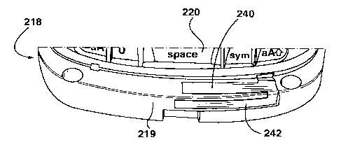
of
Figure 2 with the battery cover removed;
[0017] Figure 13 is a close up view of the antenna of the portable electronic
device
of Figure 12;
[0018] Figure 14 is a close up view of a printed circuit board of the portable
electronic device of Figure 12 having a resonator thereon; and
[0019] Figure 15 is a close up view of a low frequency shield and high-
frequency
chassis resonator of the portable electronic device of Figure 12.
DETAILED DESCRIPTION
[0020] The following describes an electronic device that includes a housing, a
touch-
sensitive display exposed by a front of the housing, and functional components
comprising memory and a processor coupled to the memory and the touch-
sensitive
display.
[0021] It will be appreciated that for simplicity and clarity of illustration,
where
considered appropriate, reference numerals may be repeated among the figures
to
indicate corresponding or analogous elements. In addition, numerous specific
details are
set forth in order to provide a thorough understanding of the example
embodiments
described herein. However, it will be understood by those of ordinary skill in
the art that
the example embodiments described herein may be practiced without these
specific
details.
CA 02731719 2011-02-15
-3-
[0022] In other instances, well-known methods, procedures and components have
not been described in detail so as not to obscure the example embodiments
described
herein. Also, the description is not to be considered as limited to the scope
of the
example embodiments described herein.
[0023] Figure 1 shows a simplified block diagram of components including
internal
components of a portable electronic device 100 according to one embodiment.
[0024] The portable electronic device 100 includes multiple components such as
a
processor 102 that controls the operations of the portable electronic device
100.
Communication functions, including data communications, voice communications,
or
both may be performed through a communication subsystem 104. Data received by
the
portable electronic device 100 may be decompressed and decrypted by a decoder
106.
The communication subsystem 104 may receive messages from and send messages to
a wireless network 150.
[0025] The wireless network 150 may be any type of wireless network,
including, but
not limited to, data-centric wireless networks, voice-centric wireless
networks, and dual-
mode networks that support both voice and data communications over the same
physical base stations.
[0026] The portable electronic device 100 may be a battery-powered device and
as
shown includes a battery interface 142 for receiving one or more rechargeable
batteries
144.
[0027] The processor 102 also interacts with additional subsystems such as a
Random Access Memory (RAM) 108, a flash memory 110, a display 112 with a touch-
sensitive overlay 114 connected to an electronic controller 116 that together
may
comprise a touch-sensitive display 118, an actuator assembly 120, one or more
optional
force sensors 122, an auxiliary input/output (I/O) subsystem 124, a data port
126, a
speaker 128, a microphone 130, short-range communications 132 and other device
subsystems 134.
[0028] In some embodiments, user-interaction with the graphical user interface
may
be performed through the touch-sensitive overlay 114. The processor 102 may
interact
with the touch-sensitive overlay 114 via the electronic controller 116.
Information, such
as text, characters, symbols, images, icons, and other items that may be
displayed or
CA 02731719 2011-02-15
-4-
rendered on a portable electronic device may be displayed on the touch-
sensitive
display 118 via the processor 102.
[0029] In some embodiments, the processor 102 may also interact with an
accelerometer 136 as shown in Figure 1. The accelerometer 136 may include a
cantilever beam with a proof mass and suitable deflection sensing circuitry.
The
accelerometer 136 may be utilized for detecting the direction of gravitational
forces or
gravity-induced reaction forces acting on the portable electronic device 100.
[0030] To identify a subscriber for network access according to the present
embodiment, the portable electronic device 100 may use a Subscriber Identity
Module or
a Removable User Identity Module (SIM/RUIM) card 138 inserted into a SIM/RUIM
interface 140 for communication with a network (such as the wireless network
150).
[0031] Alternatively, user identification information may be programmed into
the
flash memory 110 or performed using other techniques.
[0032] The portable electronic device 100 also includes an operating system
146
and software components 148 that are executed by the processor 102 and which
may
be stored in a persistent store such as the flash memory 110. Additional
applications
may be loaded onto the portable electronic device 100 through the wireless
network 150,
the auxiliary I/O subsystem 124, the data port 126, the short-range
communications
subsystem 132, or any other suitable device subsystem 134.
[0033] In use, a received signal such as a text message, an e-mail message, or
web
page download is processed by the communication subsystem 104 and input to the
processor 102. The processor 102 then processes the received signal for output
to the
display 112 or alternatively to the auxiliary I/O subsystem 124. A subscriber
may also
compose data items, such as e-mail messages, for example, which may be
transmitted
over the wireless network 150 through the communication subsystem 104.
[0034] For voice communications, the overall operation of the portable
electronic
device 100 is similar. The speaker 128 may output audible information
converted from
electrical signals, and the microphone 130 may convert audible information
into electrical
signals for processing.
[0035] Turning now to Figures 2 to 11, illustrated generally therein is a
portable
electronic device 200 according to some embodiments.
CA 02731719 2011-02-15
-5-
[0036] The portable electronic device generally includes an upper housing 202
(or
sliding portion) and a rear housing 204 (or base portion). The upper housing
202 and
lower or rear housing 204 are coupled together and are slidable between a
closed
position (as shown in Figure '2 for example) and an open position (as shown in
Figure 6
for example).
[0037] The upper housing 202 generally includes a display 206, which could be
an
LCD display and which may have touch screen capabilities. In some embodiments,
the
display 206 could be the same as or similar to the display 118 or the display
112 as
generally described above.
[0038] One or both of the upper housing 202 and lower housing 204 may include
one or more input apparatus, such as navigation keys or buttons, a physical or
virtual
keyboard, a trackpad, a trackball, multimedia keys, etc. For example, the
upper housing
202 as shown includes an auxiliary input device 212. The auxiliary input
device may be
an optical navigation module (e.g. a trackpad) that responds to user
interaction, and
which may be used for navigating around the display screen 206, to select
objects on
the display screen, or for other purposes.
[0039] In some other embodiments, the auxiliary input device 212 may be a
mechanical device that responds to user interaction (e.g. a trackball).
[0040] The display 206 and the auxiliary input device 212 are generally
disposed on
a front of the upper housing 202 and exposed for user accessibility regardless
of
whether the portable electronic device 200 is in the open or closed positions.
[0041] The upper housing 202 may also include other input devices, such as a
dedicated phone application button, a dedicated "disconnect call" button, a
home screen
button, etc. In various embodiments, these input devices may include optical
sensors,
mechanical buttons, or both.
[0042] Turning now to the rear housing 204, the rear housing 204 may include
various buttons and other controls, such as buttons 208 and 210. In some
embodiments,
buttons 208, 210 could be used for navigation, to control volume or for other
purposes.
[0043] The rear housing 204 could also include one or more application buttons
211
that can be used for example to launch a particular application on the
portable electronic
device (e.g. a camera application, a phone application, etc.). In some
embodiments, the
CA 02731719 2011-02-15
-6-
button 211 may be configurable by a user (e.g. the user may be able to select
the
particular application launched by the button 211).
[0044] As shown in Figures 2 and 6, the rear housing 204 could also include
one or
more input or output ports, (e.g. I/O ports), such as a microUSB port 214 (and
which
could be similar to or the same as data port 126). In some examples, the port
214 may
be used for data communication with the portable electronic device 200, for
charging of
a battery (not shown in Figures 2 and 6, but which could for example be
battery 144) on
the device 200 or for both.
[0045] As shown, the rear housing 204 may also include a battery cover 216 for
covering the battery (e.g. battery 144, not shown in Figures 2 and 6). In some
embodiments, the battery cover 216 may be removable. In other embodiments, the
battery cover 216 may be permanently fixed to the device.
[0046] In some embodiments, the rear housing 204 may also include an audio
jack
217. The audio jack 217 may be used to couple the portable electronic device
200 to a
speaker, amicrophone, or both, for example for use in voice communication, for
listening
to music on the portable electronic device 200, etc.
[0047] Turning now to Figures 6 to 9, as shown when the portable electronic
device
200 is in the open position, a keypad 220 is exposed on a lower portion 218 of
the rear
housing 204. The keypad 220 generally includes a plurality of alphanumeric
keys 222 for
inputting data into and otherwise controlling the portable electronic device
200. As
shown, the keys 222 may be positioned in a plurality of rows and columns. In
some
embodiments, the keys 222 may represent an alphabet and may be arranged with a
standard keyboard layout (e.g. QWERTY, QWERTZ, DVORAK, etc.) or according to
other particular patterns.
[0048] As shown in Figures 2 to 5, when the portable electronic device 200 is
in the
closed position, the keypad 220 is covered by the upper housing 202. This may
be
beneficial as it may protect the keypad 220 when not in use, and may also
inhibit
undesired keys from being pressed when the user is carrying the portable
electronic
device 200 (e.g. in a user's pocket).
[0049] In some embodiments (e.g. when the display 206 is a touchsceen), the
user
may be able to perform functions on the portable electronic device 200 while
closed by
CA 02731719 2011-02-15
-7-
interacting with the accessible input devices (e.g. using buttons 208, 210,
211, the
auxiliary input device 212, the display screen 206 itself, etc.).
[0050] When the portable electronic device 200 is in the open position (as
shown in
Figures 6 to 9), the keypad 220 is exposed for user accessibility.
[0051] In some embodiments, the display 206 may be a touch-sensitive display.
The
touch-sensitive display may be a capacitive touch-sensitive display, for
example, and a
user's touch on the touch-sensitive display may be determined by determining
an X and
Y location of the touch, with the X location determined by a signal generated
as a result
of capacitive coupling with a first touch sensor layer and the Y location
determined by
the signal generated as a result of capacitive coupling with another touch
sensor layer.
[0052] Each of the touch-sensor layers may provide a signal to a controller
that
represents the respective X and Y touch location values. Thus a feature such
as a
virtual button or other feature displayed on the touch-sensitive display may
be selected
by a mapping of the touch location to a feature on the touch-sensitive
display.
[0053] In some embodiments, the portable electronic device 200 is generally
taller
than it is wide. In such embodiments, as the portable electronic device 200
moves
between the open position and the closed position, the upper housing 202 and
rear
housing 204 move along a longitudinal axis of the portable electronic device
200.
[0054] Reference is now made to Figure 12, which illustrates a rear
perspective view
of the rear housing 204 of the portable electronic device 200 with the battery
cover 216
removed. As shown, the rear housing 204 includes a battery opening 226 for
receiving a
battery (e.g. battery 144, not shown in Figure 12).
[0055] The rear housing 204 also includes an antenna 230, which may be used
for
sending and receiving voice communications, for data communications, or both.
As
shown, the antenna 230 is provided in the lower portion 218 of the rear
housing 204. In
some embodiments the antenna 230 may be tucked behind and abut an inner
surface of
the rear housing 204.
[0056] In some examples, the antenna 230 may be a standard planar inverted F
antenna (PIFA), which may be designed to operate in various frequency bands as
desired (e.g. around 850 MHz, 1900 MHz or other frequency bands according to
the
operating characteristics of a particular wireless communication network, such
as the
wireless network 150). In some embodiments, the antenna 230 may be a LDS
surface
CA 02731719 2011-02-15
-8-
etched antenna. In some embodiments, as shown in Figure 13, the antenna 230
may
include a plastic base layer 232.
[0057] Also partially visible in Figure 12 is a printed circuit board (PCB)
234, which is
shown more clearly in Figure 14.
[0058] The PCB 234 may include various electronic components as will be
understood by a person skilled in the art, including a processor, a memory,
and a
SIM/RUIM interface 140, which may be used for receiving a SIM/RUIM and for
communication with a network such as the wireless network 150.
[0059] As shown, in some embodiments the PCB 234 also includes a PCB resonator
236. Generally, the PCB resonator 236 is configured so as to improve the high
frequency
bandwidth response for the antenna 230. In particular, the PCB resonator 236
tends to
broaden the overall high-frequency system bandwidth and thus improve antenna
230
performance.
[0060] In some embodiments, the PCB resonator 236 is generally planar, and has
an "L" shape, with a first arm portion 238, and a second arm portion 239 that
is generally
perpendicular to the first arm portion 238. In other embodiments, the PCB
resonator 236
may have other shapes and configurations.
[0061] In some embodiments, the PCB resonator 236 is an extension of a copper
ground layer of the PCB 234. In this embodiment, in the area of the "L" shaped
PCB
resonator 236, there is generally no other copper through the thickness of
that portion of
the PCB 234. This tends to inhibit interference with the PCB resonator 236,
and
facilitates increasing the high frequency bandwidth response for the antenna
230.
[0062] Turning now to Figure 15, illustrated therein are a low frequency
shield 240
and a high frequency chassis resonator 242 for the portable electronic device
200
according to one embodiment.
[0063] The inventors have observed that, when a portable electronic device
(e.g.
portable electronic device 200) with slideable housings moves between a closed
position
(e.g. as shown in Figure 2) and an open position (e.g. as shown in Figure 6),
the
effective electrical length of the chassis of the portable electronic device
changes. This
can have an impact of the sensitivity of the antenna (e.g. antenna 230),
particularly for
lower frequencies.
CA 02731719 2011-02-15
-9-
[0064] For example, as the portable electronic device 200 is moved between the
open and closed positions, this can normally result in a shift in the lower
frequency
response of about 50-60 MHz (e.g. from a base frequency of 850 MHz). In some
cases,
this can actually result in a shift from operating in one frequency band into
another
frequency band. This is generally undesirable as it can interfere with desired
operation of
the portable electronic device 200.
[0065] Accordingly, the low frequency shield 240 is sized, shaped and
configured to
act as a ground so as to anchor the response of the portable electronic device
200 and
inhibit changes to the frequency response of the antenna 230 when the portable
electronic device 200 is moved between the open position and closed position.
In
particular, in one example without the low frequency shield 240, the low
frequency
response of the portable electronic device 200 would shift lower by about
50MHz when
the portable electronic device 200 is closed; with the low frequency shield
240, this shift
can be prevented or at least greatly inhibited.
[0066] In some embodiments, the low frequency shield 240 may be a stainless
steel
sheet metal component that is attached to a stainless steel component on a
front
housing of the lower portion 218 of the rear housing 204 (e.g. by laser
welding and one
or more points, such as at two points) The sheet metal then acts as a ground
that tends
to anchor the frequency response.
[0067] Turning now to the high frequency chassis resonator 242, the high
frequency
chassis resonator 242 is generally sized, shaped and configured to assist with
higher
frequency sensitivity of the antenna 230. In some embodiments, the high
frequency
chassis resonator 242 can be a sheet metal piece with a particular length
selected (e.g.
' the length of the desired wavelength) so as to encourage higher frequency
sensitivity.
[0068] In some embodiments, the low frequency shield 240 and high frequency
chassis resonator 242 are one continuous component. For example, the low
frequency
shield 240 and high frequency chassis resonator 242 may be a continuous
stainless
steel sheet metal component that is attached to a stainless steel component on
a front
housing of the lower portion 218 by laser welding.
[0069] In other embodiments, one or both of the low frequency shield 240 and
high
frequency chassis resonator 242 may be made of other suitable materials.
[0070] In some embodiments, the low frequency shield 240 and high frequency
CA 02731719 2011-02-15
-10-
chassis resonator 242 may cooperate to shield the antenna 230 from the slider
assembly within the portable electronic device 200, and may function as a high
frequency radiating element that tends to improve high frequency efficiency
when the
portable electronic device 200 is in the closed position.
[0071] In some embodiments, at least some of the resonator and shield elements
(e.g. PCB resonator 236, the low frequency shield 240 and high frequency
chassis
resonator 242) may be tuned to work together so as to perform at least one of
inhibiting
low frequency shift and increasing high frequency sensitivity.
[0072] As shown, the low frequency shield 240 and high frequency chassis
resonator 242 may be located on a front edge 219 of the lower portion 218 of
the rear
housing 204, which is generally on the front of the portable electronic device
200
opposite the antenna 230 (which is located on the back of the portable
electronic
device). In particular, the low frequency shield 240 and high frequency
chassis resonator
242 may be located on the portable electronic device 200 near the antenna 230.
[0073] In other embodiments, other positions for the low frequency shield 240
and
high frequency chassis resonator 242 may be suitable, which may depend on the
location of the antenna 230.
[0074] In some examples, the low frequency shield 240 and high frequency
chassis
resonator 242 may be covered or concealed by part of the rear housing 204
(e.g. by a
plastic portion of the rear housing 204) during normal use so as to inhibit
the user from
contacting the low frequency shield 240 or high frequency chassis resonator
242.
[0075] While the above description provides examples of one or more processes
or
apparatuses, it will be appreciated that other processes or apparatuses may be
within
the scope of the accompanying claims.