Note: Descriptions are shown in the official language in which they were submitted.
CA 02733596 2011-02-09
WO 2010/019332 PCT/US2009/050375
ELECTRICAL CONNECTOR ASSEMBLY
TECHNICAL FIELD
The present invention relates to a high speed electrical connector assembly to
provide interconnections between a printed circuit board and one or more
electrical cables.
More particularly, the present invention relates to a shielding device that
can be included
in the electrical connector assembly to provide adequate protection from
electromagnetic
interference (EMI) emissions.
BACKGROUND
Interconnection of integrated circuits to other circuit boards, cables or
electronic
devices is known in the art. Such interconnections typically have not been
difficult to
form, especially when the circuit switching speeds (also referred to as edge
rates or signal
rise times) have been slow when compared to the length of time required for a
signal to
propagate through a conductor in the interconnect or in the printed circuit
board. As user
requirements grow more demanding with respect to circuit switching speeds, the
design
and manufacture of interconnects that can perform satisfactorily in terms of
electrical
performance has grown more difficult.
In addition, the use of faster switching speeds can be restricted by
electromagnetic
interference (EMI). EMI is a disturbance caused by electromagnetic radiation
emitted
from an external source. The disturbance may interrupt, obstruct, or otherwise
degrade or
limit the effective performance of an electrical circuit. The source may be
any object,
artificial or natural, that carries rapidly changing electrical currents.
Connectors have been developed to provide the necessary impedance control for
high speed circuits, i.e., circuits with a transmission frequency of at least
5 GHz. Although
many of these connectors are useful, there is still a need in the art for
connector designs
having closely controlled electrical characteristics as well as adequate
protection from
electromagnetic interference (EMI) emissions to achieve satisfactory control
of the signal
integrity.
SUMMARY
In one aspect, the present invention provides an electrical connector assembly
including a printed circuit board, a header coupled to the printed circuit
board, and an
electrical cable termination configured to mate with the header. The printed
circuit board
1
CA 02733596 2011-02-09
WO 2010/019332 PCT/US2009/050375
has a printed circuit board ground contact. The header includes an insulative
housing and a
plurality of contact pins disposed in the insulative housing. The header and
electrical cable
termination are configured such that the electrical cable termination makes
electrical
contact with at least one of the contact pins and the printed circuit board
ground contact
when the header and electrical cable termination are in a mated configuration.
In another aspect, the present invention provides an electrical connector
assembly
including a printed circuit board, a header coupled to the printed circuit
board, an
electrical cable termination configured to mate with the header, and a
conductive shield at
least partially enclosing the header and electrical cable termination. The
printed circuit
board has a printed circuit board ground contact. The header includes an
insulative
housing and a plurality of contact pins disposed in the insulative housing.
The header and
electrical cable termination are configured such that the electrical cable
termination makes
electrical contact with at least one of the contact pins and the printed
circuit board ground
contact when the header and electrical cable termination are in a mated
configuration.
In another aspect, the present invention provides an electrical connector
assembly
including a printed circuit board, a header coupled to the printed circuit
board, an
electrical cable assembly configured to mate with the header, and a conductive
shield at
least partially enclosing the header and electrical cable assembly. The
printed circuit board
has a printed circuit board ground contact and a printed circuit board ground
element. The
conductive shield is coupled to the printed circuit board ground element. The
header
includes an insulative housing and a plurality of contact pins disposed in the
insulative
housing. The electrical cable assembly includes an electrical cable
termination and an
electrical cable including one or more conductors and a ground shield
surrounding the one
or more conductors. The header, electrical cable assembly, and conductive
shield are
configured such that the electrical cable termination makes electrical contact
with at least
one of the contact pins and the printed circuit board ground contact, and the
conductive
shield makes electrical contact with at least one of the electrical cable
termination and the
ground shield when the header and electrical cable assembly are in a mated
configuration.
The above summary of the present invention is not intended to describe each
disclosed embodiment or every implementation of the present invention. The
Figures and
detailed description that follow below more particularly exemplify
illustrative
embodiments.
2
CA 02733596 2011-02-09
WO 2010/019332 PCT/US2009/050375
BRIEF DESCRIPTION OF THE DRAWINGS
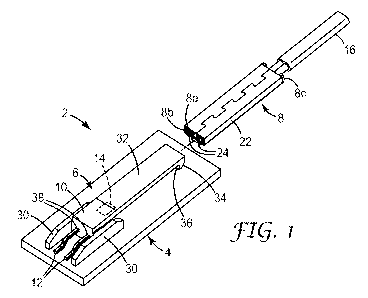
Fig. 1 is a top perspective view of an exemplary embodiment of an electrical
connector assembly according to an aspect of the present invention showing the
header
and the electrical cable termination in an unmated configuration.
Fig. 2 is a top perspective view of the electrical connector assembly of Fig.
1
showing the header and the electrical cable termination in a mated
configuration.
Fig. 3 is a cross-sectional view of the electrical connector assembly of Fig.
1 taken
along line 3-3 of Fig. 2.
Fig. 4 is a bottom perspective view of the electrical connector assembly of
Fig. 1
not showing the printed circuit board.
Fig. 5 is a top perspective view of another exemplary embodiment of an
electrical
connector assembly according to an aspect of the present invention showing the
conductive shield in an unassembled configuration.
Fig. 6 is a top perspective view of the electrical connector assembly of Fig.
5
showing the conductive shield in an assembled configuration.
Fig. 7 is a bottom perspective view of the electrical connector assembly of
Fig. 5
not showing the printed circuit board.
Fig. 8 is a top perspective view of another exemplary embodiment of an
electrical
connector assembly according to an aspect of the present invention showing the
header
and conductive shield in an unassembled configuration.
Fig. 9 is a top perspective view of the electrical connector assembly of Fig.
8
showing the header and conductive shield in an assembled configuration.
Fig. 10 is a cross-sectional view of the electrical connector assembly of Fig.
8
taken along line 10-10 of Fig. 9.
Fig. 11 is a bottom perspective view of the electrical connector assembly of
Fig. 8
not showing the printed circuit board.
DETAILED DESCRIPTION
In the following detailed description of the preferred embodiments, reference
is
made to the accompanying drawings that form a part hereof. The accompanying
drawings
show, by way of illustration, specific embodiments in which the invention may
be
practiced. It is to be understood that other embodiments may be utilized, and
structural or
logical changes may be made without departing from the scope of the present
invention.
3
CA 02733596 2011-02-09
WO 2010/019332 PCT/US2009/050375
The following detailed description, therefore, is not to be taken in a
limiting sense, and the
scope of the invention is defined by the appended claims.
For purpose of clarity, aspects of the invention are described and illustrated
herein
as used with twinaxial cables and twinaxial cable terminations. However, such
illustration
is exemplary only, and it is understood and intended that other types of
electrical cables
and their associated electrical cable terminations can be used, including but
not limited to
coaxial cables and other cable configurations with signal and ground elements.
Figs. 1-4 illustrate an exemplary embodiment of an electrical connector
assembly
according to an aspect of the present invention. Electrical connector assembly
2 includes a
printed circuit board 4, a header 6 coupled to printed circuit board 4, and an
electrical
cable termination 8 configured to mate with header 6. Header 6 includes an
insulative
housing 10 and a plurality of contact pins 12 disposed in insulative housing
10. Printed
circuit board 4 includes a printed circuit board ground contact 14. When
header 6 and
electrical cable termination 8 are in a mated configuration, electrical cable
termination 8
makes electrical contact with contact pins 12 and printed circuit board ground
contact 14,
as best shown in Fig. 3. In alternative embodiments, electrical cable
termination 8 may
make electrical contact with at least one of contact pins 12 and printed
circuit board
ground contact 14.
Electrical cable terminations that can be used in conjunction with header 6
and
printed circuit board 4 can be constructed substantially similar to the
shielded controlled
impedance (SCI) connectors for a coaxial cable described in U.S. Patent No.
5,184,965. In
particular, an exemplary embodiment of an electrical cable termination that
can be used in
conjunction with header 6 and printed circuit board 4 is electrical cable
termination 8.
Electrical cable termination 8 is coupled to header 6 such that front face 8a
of electrical
cable termination 8 abuts front surface 20a of interior wall 20 of insulative
housing 10.
Electrical cable termination 8 is coupled to an electrical cable 16 through
the use of solder
opening 18. Electrical cable 16 can be a single wire cable (e.g. single
coaxial or single
twinaxial) or a multiple wire cable (e.g. multiple coaxial, multiple
twinaxial, or twisted
pair). In one embodiment, electrical cable 16 includes one or more conductors
and a
ground shield surrounding the one or more conductors. In the embodiment of
Figs. 1-4,
electrical cable 16 includes two conductors and a ground shield surrounding
the two
conductors.
4
CA 02733596 2011-02-09
WO 2010/019332 PCT/US2009/050375
Electrical cable termination 8 includes an electrically conductive housing 22
having mounted therein internal contacts 24. Internal contacts 24 are
configured to make
electrical contact with contact pins 12 of header 6 and lie along the
longitudinal axis of
electrical cable termination 8. Each internal contact 24 can be designated as
a signal/power
contact, in which case it is electrically connected to a signal/power
conductor of electrical
cable 16 and electrically insulated from conductive housing 22. Each internal
contact 24
can be designated as a ground contact, in which case it is electrically
connected to a
ground conductor/shield of electrical cable 16 and/or to conductive housing
22.
Electrical cable termination 8 further includes an external electrical cable
termination ground contact 26. External electrical cable termination ground
contact 26
extends from an external surface of conductive housing 22 and is configured to
make
electrical contact with ground contact 14 of printed circuit board 4 when
header 6 and
electrical cable termination 8 are in a mated configuration, as best shown in
Fig. 3. In the
exemplary embodiment of an electrical connector assembly shown in Figs. 1-4,
printed
circuit board ground contact 14 includes a single ground pad. In other
embodiments,
printed circuit board ground contact 14 may include one or more ground pins,
an
electrically conductive strip, or a plurality of ground pads, as is suitable
for the intended
application. In the illustrated embodiments, external electrical cable
termination ground
contact 26 includes a resilient beam extending from conductive housing 22. In
other
embodiments, external electrical cable termination ground contact 26 can take
alternate
forms from those illustrated, and may include, for example, a Hertzian bump
extending
from conductive housing 22.
Still referring to Figs. 1-4, header 6 includes an insulative housing 10 and a
plurality of contact pins 12 disposed in insulative housing 10 and arranged
for mating with
internal contacts 24 of electrical cable termination 8. Contact pins 12 of
header 6 are
connected to printed circuit board 4 as is known in the art. Contact pins 12
are configured
for electrical connection to one or more of a plurality of electrical traces
(not shown) of
printed circuit board 4. Although header 6 is shown and described herein as a
surface-
mount pin header, header 6 may also be a through-hole pin header or any other
suitable
type of header known in the art. Contact pins 12 may be connected to printed
circuit board
4 by soldering, press-fit, or other suitable approach. In the embodiment of
Figs. 1-4,
header 6 is secured to printed circuit board 4 by the connection between
contact pins 12
5
CA 02733596 2011-02-09
WO 2010/019332 PCT/US2009/050375
and printed circuit board 4 as well as mounting posts 28 extending from
insulative housing
10. Mounting posts 28 are configured for insertion into holes in printed
circuit board 4
(not shown). Mounting posts 28 may be retained in the holes in printed circuit
board 4 by
press-fit, adhesive, or other suitable approach. Alternatively, header 6 may
include
additional structure(s) for securing header 6 to printed circuit board 4, or
may be secured
to printed circuit board 4 only by the connection between contact pins 12 and
printed
circuit board 4.
Insulative housing 10 of header 6 includes two side walls 30, an interior wall
20
positioned between side walls 30, a resilient latch 32 extending from interior
wall 20, and
mounting posts 28 extending from a bottom surface l0a of insulative housing
10.
Insulative housing 10 is monolithic, but may alternatively be formed as
multiple individual
elements (e.g., side walls 30, interior wall 20, latch 32, and mounting posts
28) assembled
by any suitable method/structure, including but not limited to snap fit,
friction fit, press fit,
mechanical clamping, and adhesive. Insulative housing 10 is configured to
receive and
position electrical cable termination 8, which is retained in a mated
configuration by latch
32. As electrical cable termination 8 is inserted into header 6, a front edge
8b of electrical
cable termination 8 engages a latch lead-in surface 34 and deflects latch 32
out of the path
of electrical cable termination 8. As electrical cable termination 8 is fully
inserted, latch 32
returns to its original (undeflected) position, and a latch hook member 36
engages a back
edge 8c of electrical cable termination 8, thereby preventing electrical cable
termination
from being pulled out of header 6. Electrical cable termination 8 can be
removed from
header 6 by simply deflecting latch 32 (as with a small tool or fingernail) to
disengage
latch hook member 36 from back edge 8c of electrical cable termination 8 while
pulling
gently on electrical cable 16. In other embodiments, electrical cable
termination 8 may be
retained within header 6 by any suitable method/structure, including but not
limited to
snap fit, friction fit, press fit, mechanical clamping, and adhesive. Interior
wall 20 of
insulative housing 10 includes a plurality of pin insertion apertures 38
configured to
position and retain contact pins 12. Contact pins 12 may be retained in
insertion apertures
38 by press-fit, friction fit, adhesive, or other suitable approach. Side
walls 30 are
configured to assist in aligning internal contacts 24 of electrical cable
termination 8 and
contact pins 12 during insertion of electrical cable termination 8 into header
6.
6
CA 02733596 2011-02-09
WO 2010/019332 PCT/US2009/050375
Additionally, side walls 30 assist in providing stability to header 6 and
protect contact pins
12 from being damaged.
Figs. 5-7 illustrate another exemplary embodiment of an electrical connector
assembly according to an aspect of the present invention. Electrical connector
assembly
102 includes a printed circuit board 4, header 6 coupled to printed circuit
board 4,
electrical cable termination 8 configured to mate with header 6, and a
conductive shield
140 at least partially enclosing header 6 and electrical cable termination 8.
Printed circuit
board 4, header 6, and electrical cable termination 8 are also illustrated in
Figs. 1-4 and
described in detail above. In this exemplary embodiment, printed circuit board
4
additionally includes a plurality of holes 142 configured to receive first
conductive shield
ground contacts 144 of conductive shield 140. When header 6 and electrical
cable
termination 8 are in a mated configuration, electrical cable termination 8
makes electrical
contact with contact pins 12 and printed circuit board ground contact 14. In
alternative
embodiments, electrical cable termination 8 may make electrical contact with
at least one
of contact pins 12 and printed circuit board ground contact 14.
Conductive shield 140 has a top wall 146 and laterally extending side walls
148a-
148d (collectively referred to herein as "side walls 148"). Although the
illustrated
embodiment includes four side walls 148 defining a substantially rectangular
box-shaped
conductive shield 140 substantially corresponding with the shape of header 6,
conductive
shield 140 may have other numbers of side walls defining other shapes as is
suitable for
the intended application. Although in the illustrated embodiment top wall 146
and side
walls 148b and 148d define a substantially rectangular transverse cross-
section, in other
embodiments, conductive shield 140 may have a generally curvilinear transverse
cross-
section. At least one of side walls 148 is configured to enable insertion and
extraction of
electrical cable termination 8. In the embodiment of Figs. 5-7, side wall 148a
extends from
top wall 146 such that it can pivot between a closed position (i.e.,
substantially
perpendicular to top wall 146) and an open position (i.e. substantially
parallel with top
wall 146). In the closed position, side wall 148a contributes to shielding of
header 6 and
electrical cable termination 8 from electromagnetic interference (EMI)
emissions. In the
open position, side wall 148a allows for electrical cable termination 8 to be
inserted into or
extracted from header 6. Similarly, side wall 148c extends from top wall 146
such that it
can pivot between a closed position (i.e., substantially perpendicular to top
wall 146) and
7
CA 02733596 2011-02-09
WO 2010/019332 PCT/US2009/050375
an open position (i.e. substantially parallel with top wall 146). In the
closed position, side
wall 148c contributes to shielding of header 6 and electrical cable
termination 8 from
electromagnetic interference (EMI) emissions. In the open position, side wall
148c allows
for access to contact pins 12 of header 6, e.g., for repair or replacement. In
part to optimize
shielding from electromagnetic interference (EMI) emissions, side walls 148a
and 148c
include flanges 154 which overlap a portion of side walls 148b and 148d. Side
wall 148a
includes an opening 152 configured to provide clearance for electrical cable
16. In one
embodiment, opening 152 in side wall 148a is shaped such as to allow insertion
and
extraction of electrical cable termination 8 without the need for side wall
148a to pivot.
Conductive shield 140 includes a plurality of first conductive shield ground
contacts 144 extending from side walls 148b and 148d. In other embodiments,
one or
more first conductive shield ground contacts 144 may extend from one or more
side walls
148. First conductive shield ground contacts 144 are configured to couple
conductive
shield 140 to a printed circuit board ground element (not shown). In the
illustrated
embodiment, first conductive shield ground contacts 144 are through-hole
contacts
configured to couple conductive shield 140 to a printed circuit board ground
element via
holes 142 by soldering, press-fit, or other suitable approach. In another
embodiment, first
conductive shield ground contacts may be surface mount contacts configured to
couple
conductive shield 140 to a printed circuit board ground element via, e.g.,
surface mount
pads on printed circuit board 4 by soldering, mechanical clamping, or other
suitable
approach.
Conductive shield 140 further includes inwardly protruding resilient second
conductive shield ground contacts 150 disposed on opposed side walls 148b and
148d.
Second conductive shield ground contacts 150 are configured to establish
electrical
contact between conductive shield 140 and electrical cable termination 8 when
header 6
and electrical cable termination 8 are in a mated configuration. In part to
optimize
shielding from electromagnetic interference (EMI) emissions, second conductive
shield
ground contacts 150 are sheared from side walls 148b and 148d, whereby
substantially all
material of side walls 148b and 148d remains present. In other embodiments,
conductive
shield 140 may include only a single second conductive shield ground contact
150.
Although the figures show that conductive shield 140 includes inwardly
protruding
resilient second conductive shield ground contacts 150, it is within the scope
of the present
8
CA 02733596 2011-02-09
WO 2010/019332 PCT/US2009/050375
invention to use other contact element configurations, such as Hertzian bumps,
in place of
resilient second conductive shield ground contacts 150.
In one embodiment, conductive shield 140 makes electrical contact with a
ground
shield of electrical cable 16 when header 6 and electrical cable termination 8
are in a
mated configuration. Electrical contact may take place directly, whereby,
e.g., side wall
148a of conductive shield 140 is in direct contact with the ground shield of
electrical cable
16 at opening 152 of side wall 148a. Electrical contact may also take place
indirectly,
whereby, e.g., second conductive shield ground contacts 150 of conductive
shield 140 is in
direct contact with conductive housing 22 of electrical cable termination 8,
which is in
direct contact with the ground shield of electrical cable 16 at solder opening
18 of
electrical cable termination 8.
In one embodiment, conductive shield 140 includes an electromagnetic
interference (EMI) absorbing material (not shown). The EMI absorbing material
is
typically used for applications requiring electromagnetic absorbing
performance. It is
designed to suppress radiated noise from electrical devices for broadband
radio frequency
range. Examples of EMI absorbing materials that can be used in an aspect of
the present
invention are EMI Absorbers AB-2000 Series or EMI Absorbers AB-5000 Series,
both
commercially available from 3M Company, St. Paul, MN. EMI Absorbers AB-2000
Series
consist of a thin, flexible backing made of silicone rubber and magnetic
materials, with an
acrylic pressure-sensitive adhesive. EMI Absorbers AB-5000 Series consists of
a flexible
soft metal flake filler in polymer resin with an acrylic adhesive system and
removable
liner. In one aspect, the EMI absorbing material can be adhered to conductive
shield 140
after cutting it to a shape that substantially corresponds with at least a
portion of the
interior surface of conductive shield 140.
In one embodiment, printed circuit board 4 includes a conductive shield
element,
such as, e.g., conductive shield element 156, shown in Fig. 5, at least
partially enclosing
header 6 and electrical cable termination 8. Conductive shield element 156 may
be formed
on printed circuit board 4 by any number of conventional deposition or etching
techniques,
such as vapor deposition, chemical etching and the like. Alternatively,
conductive shield
element 156 may be formed as a separate element from metals, conductive
polymers,
ceramics, or the like. Conductive shield element 156 may comprise, for
example, pre-
formed pieces of copper, silver, aluminum or other conductor that are
positioned on
9
CA 02733596 2011-02-09
WO 2010/019332 PCT/US2009/050375
printed circuit board 4 by soldering, press-fit, mechanical clamping, or other
suitable
approach. Conductive shield element 156 may be formed in any suitable shape,
such as,
e.g., a shape substantially corresponding with a perimeter defined by side
walls 148 of
conductive shield 140 as illustrated in Fig. 5. Conductive shield element 156
contributes to
shielding of header 6 and electrical cable termination 8 from electromagnetic
interference
(EMI) emissions. In one embodiment, conductive shield element 156 takes the
place of
printed circuit board ground contact 14, whereby external electrical cable
termination
ground contact 26 is configured to make electrical contact with conductive
shield element
156 when header 6 and electrical cable termination 8 are in a mated
configuration.
In one embodiment, electrical connector assembly 102 includes an
electromagnetic
interference (EMI) gasket (not shown) positioned around at least a portion of
conductive
shield 140 and configured to couple conductive shield 140 to a printed circuit
board
ground element (not shown). The printed circuit board ground element
facilitates electrical
grounding of electrical connector assembly 102 and can be, e.g., a plurality
of ground pads
and/or a ground trace. The EMI gasket may be positioned around conductive
shield 140 in
place of or in addition to the plurality of first conductive shield ground
contacts 144 to
facilitate substantially uninterrupted shielding around conductive shield 140.
To facilitate
easy removal of conductive shield 140 from printed circuit board 4, e.g., to
provide access
to header 6 and/or electrical cable termination 8, the EMI gasket may be
positioned around
conductive shield 140 in place of the plurality of first conductive shield
ground contacts
144. An example of EMI gaskets that can be used in an aspect of the present
invention are
XYZ-Axis Electrically Conductive Acrylic Pads (eCAP), commercially available
from 3M
Company, St. Paul, MN. eCAP products are self-stick EMI gaskets or adhesive
transfer
tapes which provide good electrical conductive path for EMI shielding and
grounding in
electronic devices. eCAP achieves a unique filler distribution in three-
dimensional
structures throughout the adhesive matrix. This filler distribution in a high
performance
adhesive makes the tape have good xyz-axis electrical conductivity and good
adhesion
performance. In one embodiment, eCAP is pre-cut into a shape substantially
corresponding with a shape defined by the edges of side walls 148 of
conductive shield
140. The pre-cut eCAP is then used to adhere conductive shield 140 to printed
circuit
board 4 (and contact the printed circuit board ground element) to form a
substantially
uninterrupted shielded interface between conductive shield 140 and printed
circuit board
CA 02733596 2011-02-09
WO 2010/019332 PCT/US2009/050375
4. Another example of an EMI gasket that can be used in an aspect of the
present
invention is a gasket fabricated from a rubber elastomer containing conductive
particulate
material. In one embodiment, the rubber gasket is formed into a rectangular-
shaped skirt
fitting around conductive shield 140. A groove is formed in the rubber gasket
which
receives the edges of side walls 148 of conductive shield 140. The rubber
gasket is
compressible and compressed between conductive shield 140 and printed circuit
board 4
(and contacts the printed circuit board ground element) to form a
substantially
uninterrupted shielded interface between conductive shield 140 and printed
circuit board
4.
If conductive shield element 156 is present, the EMI gasket may form a
substantially uninterrupted shielded interface between conductive shield 140
and
conductive shield element 156.
Figs. 8-11 illustrate another exemplary embodiment of an electrical connector
assembly according to an aspect of the present invention. Electrical connector
assembly
202 includes a printed circuit board 204, header 206 coupled to printed
circuit board 204,
electrical cable termination 8 configured to mate with header 206, and a
conductive shield
240 at least partially enclosing header 206 and electrical cable termination
8. Printed
circuit board 204 includes a plurality of holes 242 configured to receive
first conductive
shield ground contacts 244 of conductive shield 240. Electrical cable
termination 8 is also
illustrated in Figs. 1-4 and described in detail above. Header 206 includes an
insulative
housing 210 and a plurality of contact pins 212 disposed in insulative housing
210. When
header 206 and electrical cable termination 8 are in a mated configuration,
electrical cable
termination 8 makes electrical contact with contact pins 212 and conductive
shield 240.
Header 206 includes an insulative housing 210 and a plurality of contact pins
212
disposed in insulative housing 210 and arranged for mating with internal
contacts 24 of
electrical cable termination 8. Contact pins 212 of header 206 are connected
to printed
circuit board 204 as is known in the art. Contact pins 212 are configured for
electrical
connection to one or more of a plurality of electrical traces (not shown) of
printed circuit
board 204. In the embodiment of Figs. 8-11, header 206 is secured to printed
circuit board
204 by the connection between contact pins 212 and printed circuit board 204
as well as
mounting posts 228 extending from insulative housing 210. Mounting posts 228
are
configured for insertion into holes 258 in printed circuit board 204. Mounting
posts 228
11
CA 02733596 2011-02-09
WO 2010/019332 PCT/US2009/050375
may be retained in the holes in printed circuit board 204 by press-fit,
adhesive, or other
suitable approach.
Insulative housing 210 of header 206 includes two side walls 230, an interior
wall
220 positioned between side walls 230, a resilient latch 232 extending from
interior wall
220, and mounting posts 228 extending from a bottom surface 210a of insulative
housing
210. Insulative housing 210 is monolithic. Insulative housing 210 is
configured to receive
and position electrical cable termination 8, which is retained in a mated
configuration by
latch 232. As electrical cable termination 8 is inserted into header 206, a
front edge 8b of
electrical cable termination 8 engages a latch lead-in surface 234 and
deflects latch 232
out of the path of electrical cable termination 8. As electrical cable
termination 8 is fully
inserted, latch 232 returns to its original (undeflected) position, and a
latch hook member
236 engages a back edge 8c of electrical cable termination 8, thereby
preventing electrical
cable termination from being pulled out of header 206. Electrical cable
termination 8 can
be removed from header 206 by simply deflecting latch 232 (as with a small
tool or
fingernail) to disengage latch hook member 236 from back edge 8c of electrical
cable
termination 8 while pulling gently on electrical cable 16. Latch 232 further
includes a latch
opening 256 configured to enable second conductive shield ground contact 250
(described
below) to establish electrical contact between conductive shield 240 and
electrical cable
termination 8 when header 206 and electrical cable termination 8 are in a
mated
configuration. Interior wall 220 of insulative housing 210 includes a
plurality of pin
insertion apertures 238 configured to position and retain contact pins 212.
Contact pins
212 may be retained in insertion apertures 238 by press-fit, friction fit,
adhesive, or other
suitable approach. Side walls 230 are configured to assist in aligning
internal contacts 224
of electrical cable termination 8 and contact pins 212 during insertion of
electrical cable
termination 8 into header 206. Additionally, side walls 230 assist in
providing stability to
header 206 and protect contact pins 212 from being damaged.
Still referring to Figs. 8-11, conductive shield 240 is a two-part shield and
includes
a top shield portion 240a and a bottom shield portion 240b. Top shield portion
240a has a
top wall 246 and laterally extending top shield side walls 248a-248d. Bottom
shield
portion 240b has a bottom wall 247 and laterally extending bottom shield side
walls 248e-
248g. Top shield side walls 248a-248d and bottom shield side walls 248e-248g
are
collectively referred to herein as "side walls 248". Although the illustrated
embodiment
12
CA 02733596 2011-02-09
WO 2010/019332 PCT/US2009/050375
includes seven side walls 248 defining a substantially rectangular box-shaped
conductive
shield 240 substantially corresponding with the shape of header 206,
conductive shield
240 may have other numbers of side walls defining other shapes as is suitable
for the
intended application. Although in the illustrated embodiment top wall 246,
bottom wall
247 and side walls 248b/248e and 248d/248g define a substantially rectangular
transverse
cross-section, in other embodiments, conductive shield 240 may have a
generally
curvilinear transverse cross-section. In the embodiment of Figs. 8-11, top
shield side walls
248b-248d extend from top wall 246 such that they overlap with bottom shield
side walls
248e-248g when top shield portion 240a and bottom shield portion 240b are in
an
assembled configuration. When top shield portion 240a and bottom shield
portion 240b
are in an assembled configuration, top shield portion 240a contributes to
shielding of
header 206 and electrical cable termination 8 from electromagnetic
interference (EMI)
emissions. When top shield portion 240a and bottom shield portion 240b are in
unassembled configuration, electrical cable termination 8 can be inserted into
or extracted
from header 206 and contact pins 212 of header 206 can be accessed, e.g., for
repair or
replacement. In part to optimize shielding from electromagnetic interference
(EMI)
emissions, top shield side walls 248a and 248c include flanges 254 which
overlap a
portion of top shield side walls 248b and 248d. Top shield side wall 248a
includes an
opening 252 configured to provide clearance for electrical cable 16. In one
embodiment,
top shield 240a and bottom shield 240b include cooperative locking elements
260
configured to retain top shield 240a and bottom shield 240b in an assembled
configuration. In the embodiment of Figs. 8-11, top shield 240a includes
locking apertures
260a on opposing top shield side walls 248b and 248d that engage corresponding
locking
strips 260b on opposing bottom shield side walls 248e and 248g. In other
embodiments,
top shield 240a and bottom shield 240b may be retained in an assembled
configuration by
any suitable method/structure, including but not limited to snap fit, friction
fit, press fit,
mechanical clamping, and adhesive.
Conductive shield 240 includes a plurality of first conductive shield ground
contacts 244 extending from bottom shield side walls 248e and 248g. In other
embodiments, one or more first conductive shield ground contacts 244 may
extend from
one or more side walls 248. First conductive shield ground contacts 244 are
configured to
couple conductive shield 240 to a printed circuit board ground element (not
shown). In the
13
CA 02733596 2011-02-09
WO 2010/019332 PCT/US2009/050375
illustrated embodiment, first conductive shield ground contacts 244 are
through-hole
contacts configured to couple conductive shield 240 to a printed circuit board
ground
element via holes 242 by soldering, press-fit, or other suitable approach.
Conductive shield 240 further includes an inwardly protruding resilient second
conductive shield ground contact 250 disposed on top wall 246. Second
conductive shield
ground contact 250 is configured to establish electrical contact between
conductive shield
240 and electrical cable termination 8 when header 206 and electrical cable
termination 8
are in a mated configuration. In part to optimize shielding from
electromagnetic
interference (EMI) emissions, second conductive shield ground contact 250 is
sheared
from top wall 246, whereby substantially all material of top wall 246 remains
present. In
other embodiments, conductive shield 240 may include more than one second
conductive
shield ground contact 250.
In the embodiment illustrated in Figs. 8-11, bottom wall 247 includes an
optional
bridge portion 247a. Bridge portion 247a is configured to make electrical
contact with
external electrical cable termination ground contact 26 of electrical cable
termination 8
when header 206 and electrical cable termination 8 are in a mated
configuration, as best
shown in Fig. 11. In the absence of bridge portion 247a, external electrical
cable
termination ground contact 26 may be configured to make electrical contact
with a ground
contact, such as, e.g., ground contact 14 of printed circuit board 4.
In each of the embodiments and implementations described herein, the various
components of the electrical connector assembly and elements thereof are
formed of any
suitable material. The materials are selected depending upon the intended
application and
may include both metals and non-metals (e.g., any one or combination of non-
conductive
materials including but not limited to polymers, glass, and ceramics). In one
embodiment,
the electrically insulative components, such as, e.g., insulative housing 10,
are formed of a
polymeric material by methods such as injection molding, extrusion, casting,
machining,
and the like, while the electrically conductive components, such as, e.g.,
electrically
conductive housing 22, internal contacts 24, conductive shield 140, and
contact pins 12,
are formed of metal by methods such as molding, casting, stamping, machining,
and the
like. Material selection will depend upon factors including, but not limited
to, chemical
exposure conditions, environmental exposure conditions including temperature
and
14
CA 02733596 2011-02-09
WO 2010/019332 PCT/US2009/050375
humidity conditions, flame-retardancy requirements, material strength, and
rigidity, to
name a few.
Although specific embodiments have been illustrated and described herein for
purposes of description of the preferred embodiment, it will be appreciated by
those of
ordinary skill in the art that a wide variety of alternate and/or equivalent
implementations
calculated to achieve the same purposes may be substituted for the specific
embodiments
shown and described without departing from the scope of the present invention.
Those
with skill in the mechanical, electro-mechanical, and electrical arts will
readily appreciate
that the present invention may be implemented in a very wide variety of
embodiments.
This application is intended to cover any adaptations or variations of the
preferred
embodiments discussed herein. Therefore, it is manifestly intended that this
invention be
limited only by the claims and the equivalents thereof.