Note: Descriptions are shown in the official language in which they were submitted.
CA 02734133 2015-01-30
High-Speed Connector with Multi-Stacie Compensation
Background
[0002] There is a need to improve near-end crosstalk (NEXT), far-end crosstalk
(FEXT) and return loss performance of communications connectors at higher
frequencies in a robust design that can be relatively easily manufactured.
This
description is directed to a method of improving the performance of a
communication
connector by employing specific capacitive and inductive couplings on a
printed circuit
board (PCB) within the connector.
Description of the Invention
[0003] Some embodiments of the invention provide an electrical communication
jack
having improved NEXT, FEXT, and return loss performance. Additionally, this
jack
reduces the differential-to-common and common-to-differential mode conversion
(herein referred to as "mode conversion") that occurs within the jack to
improve the
alien crosstalk performance of the system.
In some embodiments, there is provided a communication jack for use in a
communication network, said jack having a plurality of plug interface contacts
for
making conductive contact with contacts of a plug, said communication jack
comprising:
eight current-carrying paths through the communication jack, said current-
carrying paths comprising first, second, third, and fourth differential pairs
of
conductors, each of said differential pairs comprising a first and a second
conductive
pathway;
compensation circuitry adapted to decrease the overall crosstalk when said
communication jack is connected to a plug, said compensation circuitry
comprising:
a first capacitor connected between the first conductive pathway of the first
differential pair and the second conductive pathway of the second differential
pair;
a second capacitor connected between the second conductive pathway of the
first differential pair and the first conductive pathway of the second
differential pair;
a third capacitor connected between the first conductive pathway of the second
differential pair and the first conductive pathway of the fourth differential
pair; and
a fourth capacitor connected between the second conductive pathway of the
second differential pair and the second conductive pathway of the third
differential pair;
1
CA 02734133 2015-01-30
wherein said first, second, third, and fourth capacitors are provided on a
flexible
circuit board in electrical contact with said plug interface contacts and
further are
provided within a single stage of compensation in said jack, and
wherein the jack further comprises a rigid circuit board containing
compensation circuitry, wherein the compensation circuitry comprises second
stage
lattice network crosstalk between the first and second differential pairs.
[00041The printed circuit board (PCB) designs described herein may be employed
in an
EIATTIA CAT6A modular jack assembly, which includes a two-stage capacitor
compensation/crosstalk with time delay, employs a version of a lattice network
as
described further below, and exhibits improved mode conversion properties. In
some
embodiments, a flex board 24 and rigid board 16, as shown in Fig. 1, work
together to
provide the desired performance characteristics of the jack.
[0005]Time delay compensation in an electrical connector achieves improved
transmission performance for near-end crosstalk by introducing predetermined
amounts
of compensation and crosstalk between two pairs of conductors that extend from
the
connector's input terminals to its output terminals along interconnection
paths.
Electrical signals on one pair of conductors are coupled onto the other pair
of
la
CA 02734133 2011-02-14
WO 2010/022231 PCT/US2009/054454
conductors in two or more compensation stages that are time delayed with
respect to
each other. Generally, in a first stage the compensating crosstalk nearer to
the plug is
of an opposite magnitude of the net crosstalk caused by the plug. The second
stage of
crosstalk is generally of the same polarity as the net crosstalk caused by the
plug, and
is placed further away from the plug than the first stage. The differing time
delays
between the stages cause the phases of these stages to change at different
rates with
increasing frequency. This then creates a specific frequency where all of the
stages
add together to essentially cancel out and create a null, which in turn
increases the
overall NEXT bandwidth of the mated plug and jack.
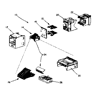
[0006] According to one embodiment of the present invention, a CAT6A RJ45 jack
10
has a housing 12 that fits an RJ45 plug, a nose 14 that has eight plug
interface contacts
(PICs) that mate with a plug and interface with a rigid board 16, where the
rigid board
16 connects to insulation displacement contacts (IDCs) 18, a rear sled 20 that
holds the
IDCs, and a wire cap 22 that allows for wires within cabling (not shown) to
connect with
the IDCs. The nose 14 also includes a flex circuit board 24, plug interface
contacts 26,
front bottom sled 28 and front top sled 30. Both the flex circuit board 24 and
rigid circuit
board 16 contain circuitry designed to improve NEXT, FEXT, return loss, and
mode
conversion properties of the jack.
[0007] CAT6A products generally have eight wires that make up four
differential pairs.
These wires are numbered numerically 1 through 8, and the differential pairs
are 45, 36,
12, and 78 (pairs 1, 2, 3, and 4, respectively). The layout of these wires
within an RJ45
plug causes crosstalk between these differential pairs that must be
compensated for
within a jack. Since there are four differential pairs, near end crosstalk
(NEXT) can form
between the six different pair combinations. These pair combinations are 45-
36, 45-12,
45-78, 36-12, 36-78, and 12-78. In different embodiments of the present
invention,
compensation is achieved by positioning traces on circuit boards within a
jack.
[0008] Self-inductive stubs as used herein (shown in Figs. 2, 6-8, and 13-15)
refer to
circuit board traces that are made specific lengths to create a self-
inductance of a given
value. The term "stub" refers to the fact that these traces are not part of
the main
current carrying path. They are stubs off of the current carrying path, and
end in a
2
CA 02734133 2011-02-14
WO 2010/022231 PCT/US2009/054454
capacitor (having no DC connections at their ends). Current carrying paths are
traces
that allow a DC current to flow between two points (such as the RJ45 plug and
the
insulation displacement contacts 16 (IDCs) in the jack).
[0009] A lattice network as described herein generally includes a crosstalk
circuit
component and a compensation circuit component each of which has a different
coupling rate versus frequency. A "crosstalk circuit component" is a circuit
component
in which coupling occurs with the same polarity as the crosstalk-producing
coupling
within a plug, while a "compensation circuit component" is a circuit component
in which
coupling occurs at a polarity that is opposite the polarity of the crosstalk
coupling that
occurs within a plug.
[0010]The version of the lattice network used in this invention adds a second
self-
inductive stub connected between a capacitor and the second signal trace to
the 2nd
stage crosstalk network. Previous designs have employed what could be called
an "LC"
circuit, having most of the inductance attached to one end of the capacitor.
The design
of one embodiment of the current invention could be termed an "LCL" circuit,
having the
inductor split such that significant inductances are used on both sides of the
capacitor.
[0011]Self-inductive stubs, as described herein, use the distributed
electrical parameter
of inductance per unit length of the circuit trace to produce inductive
elements.
Although this is modeled in the schematics as a discrete inductor (which is
appropriate
as it has an equivalent effect) it is a distributed inductive component
produced by the
length of the traces as opposed to turns of a wire coil, for example. In
contrast, the
capacitors shown herein are discrete capacitors although both the capacitors
and the
inductors shown can be realized by discrete or distributed components, or as a
combination thereof.
[0012] Positioning a capacitor between two stubs improves NEXT performance,
relative
to the opposite transmission direction (IDC to PIC), compared to putting a
single
inductor on only one side of that capacitor, where the inductance of the
single inductor,
L1, is about equal to L2 + L3 as shown in Fig. 2. Additionally, the second
stub shows
improvement in return loss, also relative to using only a "one-sided"
inductor.
3
CA 02734133 2011-02-14
WO 2010/022231 PCT/US2009/054454
[0013]The self inductive stubs, along with corresponding capacitors (for
example, the
L5-056-L6 combination and L3-C34-L4 combination as shown in Fig. 6), may be
modeled as an LC circuit with a resonance effect having a resonant frequency
of
f0=1/(2-rrA1LC). The selection of the inductance and capacitance values (i.e.,
the Ls and
the Cs) is generally a nonlinear multivariable optimization with multiple
objective
functions, (the "objective functions" being improved NEXT, FEXT, return loss,
etc.).
Consequently, selection of a given L or C value is not made independent of
other circuit
considerations. Some of the considerations for selecting a given L value
include: if it is
too low the resonance point moves to a higher frequency and there is no
desired NEXT
improvement in the signal frequency operation range of interest; if the
inductance is too
high: a) the inductive traces become too long to fit on a typical rigid board;
b) the
resonance can move into the frequency operation range of interest, possibly
introducing
deleterious effects; and c) there can be a degradation of return loss.
[0014]The general design of a CAT 6A jack according to one embodiment of the
present invention uses a two-stage capacitor compensation/crosstalk with time
delay for
pair combinations 45-36, 36-12, 36-78, and 45-12. The flex board 24 contains
the first
stage capacitors in the time delay model for pair combinations 45-36, 36-12,
and 36-78
(the flex board includes capacitors C35, C45, C26, and C37). The rigid board
16 then
contains the second stage capacitors in the time delay model for specific pair
combinations (C46, C56, C16, and C38). The combination of a flex board 24 and
a rigid
board 16 for pair combination 45-36 also includes a lattice network which
additionally
uses self-inductors L3, L4, L5, and L6 and the additional capacitors C35 and
C46 on the
rigid board 16 (there is no lattice network on any other pairs for this
embodiment).
[0015]This description takes into account the following:
= All capacitor dimensions given are referenced relative to the amount of
overlap
occurring between the pads. One conductive layer of each capacitor is
oversized
mils to help account for layer-to-layer registration. The dimensions given are
for the smaller layer. According to one embodiment, rigid board capacitors are
formed across a 4 mil core, generally made of an FR4 material having a
dielectric
constant of approximately 4.4. Flex board capacitors are formed across a 1 mil
4
CA 02734133 2011-02-14
WO 2010/022231 PCT/US2009/054454
core, generally made of a material having a dielectric constant of
approximately
3.4.
= The schematics shown for each description include only the intentional
capacitance added by design. For example, mutual inductance between wires is
purposely not shown for schematic clarity and due to the fact that any mutual
inductance that results from the design is not intentionally used for
compensation.
= These schematics do not show parasitic capacitances caused by the
geometry of
the setup unless this parasitic capacitance is deemed important to note
(values
greater than 0.1 pF). These values are noted, but not labeled with reference
characters.
= The schematics shown for each pair combination (Figs. 9-13) do not show
all
connections since they are only showing two pairs at once. A full schematic of
the rigid board 16 can be seen in Fig. 6.
= The distance causing a time delay from the flex board to the PIC
interface on the
rigid board is approximated as 0.5" for all pair combinations.
= The schematics shown attempt to approximate a "middle plug" which by
definition per the EIA/TIA CAT6A standards refers to a plug whose crosstalk
value is in the middle of the range of crosstalk values specified for that
pair
combination.
= All circuit board dimensions described herein are each individually
subject to
change (estimates up to 20%). One reason for this is variability of circuit
board
build tolerances from different circuit board manufacturers. Different
materials or
different processes may be used to manufacture the circuit boards. Therefore,
the performance of the circuit board may change even though the artwork is
identical due to the capacitance changing. Another reason is to allow for
design
changes required to compensate the many different jack designs (for example,
modular jacks, shielded jacks, and unshielded jacks). Consequently, good
engineering practice requires the ability to change the area of overlap for
the pad
capacitors by the specification tolerance ( 20%). This change in area may be
done on a capacitor-by-capacitor basis, and the overall board design (trace
CA 02734133 2011-02-14
WO 2010/022231 PCT/US2009/054454
layout, use of time delay, lattice) remains identical. Some variants may only
require changing the size of one or two capacitors (either smaller or larger),
and
some may require changing the sizes of all capacitors.
= The jack designs described herein can be used for several types of
products,
among them shielded, unshielded, and punchdown-type connectors. Further, the
jack housing 12 or another component of the jack may be covered with a
conductive foil to reduce alien crosstalk effects.
Flex Circuit Board
[0016] The flex circuit board 24 shown in Fig. 1 is described in more detail
in Figs 3-5.
Fig. 3 shows a schematic diagram of the flex circuit board, Fig. 4 shows the
traces
provided on two conductive layers of the flex circuit board, and Fig. 5 is a
perspective
view of the flex circuit board in which both layers of conductive traces are
visible. The
flex circuit board contains the 1st stage compensation in the time delay model
for pair
combinations 45-36, 36-12, and 36-78. This is done by the flex circuit board
24
employing pad capacitors to add compensating crosstalk having a polarity
opposite that
of the plug. These pad capacitors are C46 and C35 for pair combination 45-36,
C26 for
pair combination 36-12, and C37 for pair combination 36-78. Additionally, the
capacitance values of the capacitors are chosen so that the mode conversion
across
the pairs 45-36, 36-12, and 36-78 is reduced.
[0017] Referring to Figs. 3-5, the flex circuit board has the following
features:
1) The flex board 24 wraps around the nose 14 such that the top layer of the
flex
board makes contact with the PICs (the area where contact is made is
highlighted in Fig. 5).
2) Crosstalk compensation with a polarity opposite that of the plug for pair
combination 45-36 is provided by pad capacitors C35 and C46. The area of
each pad capacitor is 0.0323" by 0.044" ( 20%), and each has a capacitance of
approximately 1.2 pF. The schematic for pair combination 45-36 can be seen in
Fig. 13.
6
CA 02734133 2011-02-14
WO 2010/022231 PCT/US2009/054454
3) Crosstalk compensation with a polarity opposite that of the plug for pair
combination 36-12 is provided by pad capacitor C26. The area of this pad
capacitor is 0.03" by 0.033" ( 20%), and the capacitor has a capacitance of
approximately 0.85 pF. The schematic for pair combination 36-12 can be seen in
Fig. 11.
4) Crosstalk compensation with a polarity opposite that of the plug for pair
combination 36-78 is provided by pad capacitor C37. The area of this pad
capacitor is 0.03" by 0.033" ( 20%), and the capacitor has a capacitance of
approximately 0.85 pF. The schematic for pair combination 36-78 can be seen in
Fig. 12.
Rigid Circuit Board 16
[0018]The rigid circuit board 16 shown in Fig. 1 is illustrated in more detail
in Figs. 6-8.
Fig. 6 shows a schematic view of the rigid circuit board, Fig. 7 shows
conductor layouts
on different layers of the board, and Fig. 8 is a "see-through" perspective
view showing
all of the conductive layers of the board. The rigid circuit board 16 contains
the 1st and
only stage of crosstalk compensation for pair combination 45-78. It contains
both the 1st
and 2nd stage of time delay crosstalk for pair combination 45-12.
Additionally, it
contains the 2nd stage of crosstalk in the time delay model for pair
combinations 36-12
and 36-78. It also contains the 2nd stage lattice network crosstalk for pair
combination
45-36. The method of adding capacitors on the rigid board is chosen so that
the mode
conversion across all pairs is reduced.
[0019] Referring to Figs. 6-8, one embodiment of the rigid circuit board has
the following
features:
1) This rigid board design incorporates non-plated holes drilled into the
board (some
are highlighted in Fig. 8). These holes are used to reduce the distributed
capacitance between wires 4 and 5; and 3 and 6 by lowering the effective
dielectric constant between respective traces through the addition of air gaps
so
that the return loss on these pairs is further improved. This "variable
dielectric"
over the length of a trace can be used to improve performance of the jack.
7
CA 02734133 2011-02-14
WO 2010/022231 PCT/US2009/054454
2) Current carrying traces are routed between PIC vias and IDC vias with the
respective pin numbers. PIC vias refer to the vias where the compliant pins
from
nose 14 interface with the rigid circuit board 16, shown in Fig. 1. The IDC
vias
refer to the vias where the IDCs 18 interface with the rigid circuit board 16.
3) Crosstalk having the opposite polarity of the net crosstalk caused by the
plug for
pair combination 45-78 is provided by pad capacitor C47 connected between the
4 and 7 PIC vias, and by pad capacitor C58 connected between the 5 and 8 PIC
vias. Both of these capacitors have areas of 0.02" by 0.02" ( 20%). A
schematic for pair combination 45-78 is shown in Fig. 9.
4) Crosstalk compensation for pair combination 45-12 is achieved by using the
time
delay model. A schematic for pair combination 45-12 is shown in Fig. 10. Pad
capacitor C14 has the opposite polarity from the net crosstalk caused by the
plug
for pair combination 45-12 and connects between PIC vias 1 and 4. Pad
capacitor C15 has the same polarity as the net crosstalk caused by the plug
for
pair combination 45-12 and connects between IDC vias 1 and 5. C15 is time
delayed from C14 by approximately 0.395" (average distance between the 1, 2,
4, and 5 PIC vias to their respective IDC vias). The area of the pad capacitor
C14 is 0.021" by 0.021" 20%, and the area of the pad capacitor C15 is 0.028"
by 0.028" 20%.
5) Crosstalk compensation for pair combination 36-12 is achieved by a pad
capacitor C16 having the same polarity as the net crosstalk caused by the
plug.
It is connected between PIC via 1 and IDC via 6. This pad capacitor works in
tandem with the pad capacitor C26 on the flex circuit board using the time
delay
method to achieve NEXT performance exceeding 500 MHz for pair combination
36-12. The area of pad capacitor C16 is 0.035" by 0.061" ( 20%). The
schematic for pair combination 36-12 can be seen in Fig. 11.
6) Crosstalk compensation for pair combination 36-78 is achieved by a pad
capacitor C38 having the same polarity as the net crosstalk caused by the
plug.
It is connected between IDC via 3 and IDC via 8. This pad capacitor works in
tandem with the pad capacitor C37 on the flex circuit board using the time
delay
method to achieve good NEXT performance at frequencies exceeding 500 MHz
8
CA 02734133 2011-02-14
WO 2010/022231 PCT/US2009/054454
for pair combination 36-78. The area of pad capacitor 038 is 0.01" by 0.01" (
20%). The schematic for pair combination 36-78 can be seen in Fig. 12.
7) Crosstalk compensation for pair 45-36 is achieved by a lattice compensation
technique. This lattice network includes the following:
a. A pad capacitor 035 having opposite polarity from the net crosstalk
caused by the plug for pair combination 45-36 connected between PIC
vias 3 and 5. The pad capacitor area is .013" by .013" ( 20%).
b. A capacitor 046 of approximately 0.2 pF having opposite polarity from the
net crosstalk caused by the plug for pair combination 45-36 which is
created by the capacitance between trace 4 (leading to the 047 capacitor)
and PIC via 6 (shown in Fig. 8). A small pad capacitor could be added
here if the process, manufacturing, or engineering designs require it, but
this capacitor's size should remain under 0.02" by 0.02".
c. A pad capacitor 034 having same polarity of the net crosstalk caused by
the plug for pair combination 45-36 is connected between wires 3 and 4
utilizing a self-inductive stub L3 of approximately 0.8" in length running
between PIC 3 and the 034 pad capacitor. The other pad of the 034
capacitor terminates another self-inductive stub L4 of approximately 0.8"
in length, which leads to a via on current carrying trace 4. The area of
pad capacitor 034 is .029" by .029" ( 20%).
d. A pad capacitor 056 having the same polarity as the plug for pair
combination 45-36 is connected between conductors 5 and 6 utilizing a
self-inductive stub L6 of approximately 1.1" in length. The self-inductive
stub L6 is connected to PIC 6, and runs to the 056 pad capacitor with time
delay. The other pad of the 056 capacitor is connected to another self
inductive stub L5 of approximately 0.8" in length, which runs to a via on
current carrying trace 5. The area of pad capacitor 056 is .03" by .03" (
20%).
e. The reason inductive stubs L4 and L5 do not connect directly to the PIC
vias is that this allows for improved return loss in the jack by adding
additional length away from the PICs.
9
CA 02734133 2011-02-14
WO 2010/022231
PCT/US2009/054454
f. The
schematic for pair combination 45-36 can be seen in Fig. 13, which
further illustrates the lattice network used in this design.
Description of Overall Jack Compensation Technique for Each Pair Combination
[0020]This section describes how the flex board 24 and rigid board 16 work
together in
one embodiment of a jack.
Pair Combination 45-78
[0021]The schematic for pair combination 45-78 is shown in Fig. 9. The
compensation
technique on pair combination 45-78 does not use the flex board for any of its
capacitors. It does not use the time delay or lattice network techniques
either.
Pair Combination 45-12
[0022]The schematic for pair combination 45-12 is shown in Fig. 10. The
compensation technique on pair combination 45-12 does not use the flex board
for any
of its capacitors. It does not use the lattice network either. However, it
does make use
of the time delay method by having C15 time delayed by approximately 0.395"
(average
distance between the 1, 2, 4, and 5 PIC vias to their respective IDC vias)
from C14 (with
both capacitors on rigid board 24).
Pair Combination 36-12
[0023]The schematic for pair combination 36-12 is shown in Fig. 11. It
includes
capacitor C26 on flex board 24 and C16 on rigid board 16. C16 is time delayed
by
approximately 0.68" from the C26. This includes the 0.5" length from the flex
board to
the PIC rigid board interface, and an additional length of 0.18" on the rigid
board (based
on half the distance between the 3 and 6 PIC vias and their respective IDC
vias since
the connection for pair 1 is on the PIC via whereas the connection for pair 6
is on the
IDC via). There is no lattice network used on pair combination 36-12.
Pair Combination 36-78
[0024]The schematic for pair combination 36-78 is shown in Fig. 12. It
includes
capacitor C37 on flex board 24 and capacitor C38 on rigid board 16. C38 is
time
CA 02734133 2011-02-14
WO 2010/022231 PCT/US2009/054454
delayed by approximately 0.75" from 037. This includes the 0.5" length from
the flex
board to the PIC rigid board interface, and an additional length of 0.25" on
the rigid
board (based on half the distance between the 3, 6, 7, and 8 PIC vias and
their
respective IDC vias). There is no lattice network used on pair combination 36-
78.
Pair Combination 45-36
[0025] The schematic for pair combination 45-36 is shown in Fig. 13. It
includes
capacitors C35 and C46 on flex board 24. It also includes C35, C46, C34, C56,
L3, L4,
L5, and L6 on the rigid circuit board 16. Capacitors C34 and C56 are time
delayed from
the flex circuit board capacitors C35 and C46 by approximately 0.56". This
includes the
0.5" length from the flex board to the PIC rigid board vias, and an additional
length of
0.06" on the rigid board (based on half the distance between the 4 and 5 PIC
vias and
the plated through hole vias where the stubs associated with conductors 4 and
5 tap
off). The combination of the capacitors on the flex circuit board 24, the
capacitors on
the rigid board 16, and the inductors comprises a lattice network. The
addition of
inductors L3, L4, L5, and L6 with C34 and C56 create a frequency-dependent
vector
that grows at a faster rate with frequency than the crosstalk caused by the
C35 and C46
capacitors. This in turn allows for additional bandwidth on 45-36 NEXT up to
and
exceeding 500 MHz.
Additional Embodiments of Rigid Board 16
Additional Embodiment 1: Adjusting Trace Geometry
[0026] This embodiment, which gains additional NEXT bandwidth on pair
combination
36-78, is shown in Fig. 14. This embodiment incorporates all aspects of the
design
described elsewhere herein except for the differences highlighted. The main
reason for
this change in routing is to reduce the parasitic capacitance between contacts
6 and 8
that can occur with L6. Note that several capacitor sizes are slightly changed
to
account for the new layout but stay within the aforementioned tolerance
ranges. Also
note that a C68 capacitor may be added to the design to allow this rigid
circuit board to
work with the flex board described in Figs. 3-5. The schematic for this 36-78
pair
11
CA 02734133 2011-02-14
WO 2010/022231 PCT/US2009/054454
combination is similar to Fig. 12, with the exception that the 0.25 pF
parasitic
capacitance on the rigid board has been made slightly smaller.
Additional Embodiment 2: Adjusting Trace
Geometry and Balancing Capacitance on Pair 45-12
[0027] This embodiment, which gains additional NEXT bandwidth on pair
combination
36-78, is shown in Fig. 15. This embodiment incorporates all aspects of the
design
described elsewhere herein, including both the main description and Additional
Embodiment 1, except for the differences highlighted. The main reason for this
change
was to improve the mode conversion across pair combination 45-12 by adding
C25.
Note that several capacitor sizes are slightly changed to account for the new
layout. A
schematic for 45-12 is shown in Fig. 16. Note that for this schematic, C14,
C25, C15,
and C24 are all closer in their net value across the schematic which will
result in
improved mode conversion characteristics.
12