Note: Descriptions are shown in the official language in which they were submitted.
CA 02736292 2011-03-07
WO 2010/025536 PCT/CA2008/001562
Thin Film Optical Filters with an Integral Air Layer
Field of the Invention
This invention relates to the field of optical filters, and in particular
optical filters
employing thin film interference and frustrated total internal reflection
(FTIR).
Background of the Invention
Thin film optical filters are often used in applications that require light
incident at the
filter surfaces at non-normal or oblique angles of incidence in order to
generate two beams: a
reflected beam and a transmitted beam. Such optical filters include thin film
polarizing beam-
splitters, non-polarizing beam-splitters, long-wavelength and short-wavelength
cut-off filters,
bandpass filters, etc. Often these thin film optical filters consist of
multiple layers between two
solid glass substrates or prisms. One arising issue with optical filters used
at oblique angles of
incidence is the polarization effect for s- and p-polarized light due to their
different optical
admittances at oblique angles. This polarization effect is manifested as
different filter properties
for s- and p-polarized light, such as different reflectance, transmittance, or
phase changes on
reflection or transmission. For polarizing beam-splitters, the polarization
effect needs to be
enhanced in order to reflect light in s- or p-polarization and transmit light
in p- or s-polarization.
For many other optical filters such as non-polarizing beam-splitters, cut-off
filters and bandpass
filters, the polarization effect is not desirable and must be minimized.
Using thin film interference effect alone to either enhance or minimize
polarization
effect in these optical filters often does not produce satisfactory results.
However, it has been
demonstrated that the phenomenon of frustrated total internal reflection can
be combined with
thin film interference to successfully control the polarization effect in
polarizing and non-
1
CA 02736292 2011-03-07
WO 2010/025536 PCT/CA2008/001562
polarizing thin film beam-splitters. In particular, high-performance thin film
polarizing beam-
splitters operating at angles greater than critical angle and having all solid
films were disclosed
in US. Patent No. 5,912,762 and in the paper by Li Li and J. A. Dobrowolski, "
High-
performance thin-film polarizing beam splitter operating at angles greater
than the critical
angle," Appl. Opt. Vol. 39, pp2754-2771 (2000). In addition, in the paper by
Li Li "Design of
thin film optical coatings with frustrated total internal reflection", Optics
and Photonics News,
September 2003, pp24-30 (2003), it also has been shown that the FTIR effect
can be used to
minimize polarization effects in non-polarizing beam-splitters having solid
layers as described.
Traditional FTIR filters consist of solid thin film layers that are made of
solid materials
and are deposited by physical or chemical vapour deposition techniques. The
use of FTIR effect
requires that the incident angles inside the lowest refractive index nL layers
in the filter coatings
be greater than that of the critical angle 0C, which is defined as:
BC = aresin(n`) , (1)
no
where no is the refractive index of the substrate.
There are several problems with using the FTIR effect in thin film optical
filters having
solid layers. First, because the selection of low index coating materials is
limited and the
refractive index values are not as low as one would prefer, usually 1.38 for
MgF2 and 1.45 for
Si02, which leads to a very large critical angle Oc. For example, when
no=1.52, nL=1.45,
OC=72.5 . The large 0C will result in large working angles for the thin film
optical filters, which
in turn results in large size filters. Large size optical filters are not
desirable for many
applications. Second, although the critical angle can be reduced by using high
index substrates
2
CA 02736292 2011-03-07
WO 2010/025536 PCT/CA2008/001562
(for example, no>l .60), more, complicated or expensive optical bonding
technique have to be
used to cement the two substrates together.
It is generally very difficult to bring two coated high refractive index
prisms into good
contact. Index matching optical cements, which are commonly used in the optics
industry, are
not suitable for this purpose because stable and highly transparent
(transmittance >95%) optical
cement with a refractive index greater that 1.60 is not available. Refractive
index-matching
liquids are also not suitable because they are usually not stable and require
proper sealing and
thickness control. Furthermore refractive index-matching liquids with
refractive indices greater
than 1.80 usually contain very toxic materials, such as arsenic. In addition,
for the infrared
spectral region, there are practically no optical cements transparent for the
infrared spectral
region from 2 m to 30 m. Thus, the only suitable optical bonding technique is
very expensive
optical contacting.
Optical contacting is a well-established technique that has been used in
optical shops for
many years. The principle of optical contacting is that if the two contacting
surfaces are flat and
smooth enough, a van der Waals bond (sometimes with assistance from chemical
bonding) will
hold them together. To form a strong van der Waals bond, the surfaces of the
substrates have to
be polished very smooth with a flatness to be at least 1/10, where ? is the
wavelength of light
used to measure the flatness of the surfaces and a, is usually in the visible
and about 630nni.
This strict flatness requirement increases the manufacturing cost. Poor
coating quality such as
roughness can further reduce the success rates of optical contacting. The
difficulty of achieving
a good optical contact is directly proportional to the area of the surfaces to
be contacted. The
larger the component surfaces, the more difficult it is to make their surfaces
sufficiently flat and
smooth for optical contact. In addition, for optical filters in the infrared
spectral region, because
3
CA 02736292 2011-03-07
WO 2010/025536 PCT/CA2008/001562
the optical filters are much thicker compared to the visible spectral region,
the filter coatings are
usually deposited by a much faster evaporation process that inherently
produces rough and
porous films, making optical contacting even more difficult.
The use of an air layer or gap has been described in tuneable Fabry-Perot
filters. In these
filters, the air gap allows the layer thickness to be varied in order to tune
the filter properties, for
example, to change the pass band wavelength. In such tuneable filters, the low
refractive index
of the tuning air layer is not of any significance. Another use of an air gap
within thin film
systems occurred the late 1960-ties, in resonant reflectors, in which thin,
self-supporting silica
or sapphire plates were spaced with air to form reflectors that survived high
power laser
irradiation. In both instances light is incident at normal angle of incidence
(0 ) and prisms are
not used and not FTIR effect occurs. Moreover, in each case there was a
specific reason to
employ an air gap specific to, the particular product.
The use of an air gap as a medium in birefringent polarizers is known. It has
also been
recently proposed in the US patent Application Nos. US20030112510 and
US20060098283 to
form metal grid polarizing beam-splatters. These polarizers and polarizing
beam-splitters are
based on different physical principles than that of the present invention. No
light interference or
frustrated total internal reflection is employed in these devices.
Summary of the Invention
According to one aspect of the present invention there is provided an optical
device
comprising an optical device comprising: a pair of transparent substrate
prisms having
opposing faces bonded together at an interface; a thin film interference
structure between said
pair of transparent substrate prisms; and a spacer layer located between said
opposing faces,
4
CA 02736292 2011-03-07
WO 2010/025536 PCT/CA2008/001562
said spacer layer separating said transparent substrates to form a cavity
containing low
refractive index layer comprising a non-reactive gas or vacuum; and wherein
said low
refractive index layer in said cavity acts as an interference layer forming an
integral part of
said thin film structure, and wherein said thin film structure is operable to
permit thin film
interference coupled with frustrated total internal reflection inside said low
index layer at
certain angles of incidence.
The thin film interference structure will normally consist of a plurality of
coatings
deposited on at least one of the opposing faces, but in the extreme case it
would be possible to
construct a thin film interference structure consisting only of one coating
and the low refractive
index layer.
It will be understood that the thickness of the layers in the "thin" film
structure is
commensurate with the wavelength of the light for which the device is designed
to operated so that
thin film interference effects occur.
The embodiments of the invention effectively control the polarization effects
with an
integral air layer in thin film optical filters that operate at oblique angles
greater than the critical
angel. The air layer which is defined by a spacer layer permits the easy
fabrication of high-
performance thin film optical filters with reduced cost. In addition, compared
to traditional thin
film optical filter having all solid films, these embodiments have much
improved performances,
or smaller prism size because the angles of incidence can be reduced with the
use of low index
air layer, or reduced total number of layers or layer thickness, or all of the
above.
The use of an air gap as a medium as known in the prior art is very different
from
using an air gap, or more precisely air layer, as an integral part of thin
film interference filters
CA 02736292 2011-03-07
WO 2010/025536 PCT/CA2008/001562
in the present invention. First of all, unlike the invention, such an air gap
is generally very
thick compared to the wavelength of the light and is treated as a medium
rather than an
interference thin film. Its thickness does not affect the performance of the
device and because
it is so thick that no light interference occurs between the light reflected
from the two air
substrate interfaces because the optical path length is longer than the
coherence length of
most light sources. Second, the incident angle for the desired polarization is
smaller than the
critical angle, so no frustrated total internal reflection or total internal
reflection occurs inside
the air gap. If the incident angle on these devices were greater than the
critical angle, all light
would be reflected, no light would be transmitted and the device would not
work at all. In the
present invention, the cavity layer is treated as an integral part of the thin
film interference-
frustrated total internal reflection structure, and has a layer thickness
commensurate with this role.
It will be understood that references to light and "optical" in this
specification are not
limited to the visible region. The invention is applicable to all wavelengths,
for example, W,
visible, infrared and millimemeter wavelength region susceptible to filtering
and
combining/splitting by the prism devices described.
According to another aspect of the invention there is provided a method of
making an
optical device comprising: providing a pair of transparent substrate prisms
having opposing
faces; forming a thin film interference structure between said pair of
transparent substrates
configured to subject light incident on one of said substrates at certain
angles of incidence to
thin film interference coupled with frustrated total internal reflection; and
bonding opposing
faces together through a spacer layer, said spacer layer separating said
transparent substrates
to form a low refractive index cavity layer that acts as an interference layer
forming an
integral part of said thin film interference structure.
6
CA 02736292 2011-03-07
WO 2010/025536 PCT/CA2008/001562
Brief Description of the Drawings
The invention will now be described in more detail, by way of example only,
with reference to
the accompanying drawings, in which:
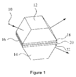
Figure 1 shows a thin film optical filter having an integral air layer;
Figure 2 is an expanded view of.the thin film optical filter structure;
Figure 3 shows a thin film optical filter having an integral air layer with
different spacer
patterns;.
Figure 4 shows a thin film optical filter having an integral air layer with
additional side
panels;
Figure 5 shows a simple thin film optical filter Si having two high index
substrates and a
single air layer;
Figure 6 shows the calculated transmittance of s- and p-polarized light with
angle of
incidence for the above filter Si with no=1.75, nj=1.0 and a layer thickness
dt=50nm at
wavelength 2=550nm;
Figure 7 shows the calculated transmittance of s- and p-polarized light with
angle of
incidence for the above filter Si with n0=1.75, nl=1.0 and a layer thickness
d1=100nm at
wavelength 2=550nm;
Figure 8 shows the calculated transmittance of s- and p-polarized light with
angle of
incidence for the above filter SI with no=1.75, n1=l .0 and a layer thickness
dl=200nm at
wavelength 2=550nm;
7
CA 02736292 2011-03-07
WO 2010/025536 PCT/CA2008/001562
Figure 9 shows the calculated transmittance of s- and p-polarized light with
angle of
incidence for the above filter Si with no=1.75, n1=1.0 and a lay-r thickness
d1=500nm at
wavelength 2=550nm;
Figure 10 shows the calculated transmittance of s- and p-polarized light with
angle of
incidence for the above filter Si with no=1.75, n1=1.0 and a layer thickness
d1=1000nm at
wavelength 2=550nm for s- and p-polarized light;
Figure 11 shows the calculated transmittance of s- and p-polarized light with
angle of
incidence for a filter similar to Si but with no=1.75, n1=1.0 the. air layer
is treated as a
medium rather than a thin film at wavelength 2=550nm;
Figure 12 shows the calculated transmittance of s- and p-polarized light with
angle of
incidence f o r a simple optical filter similar to S 1 but having no=1.75,
n1=1.45 and d1=50nm
with a layer medium at wavelength A=550nm;
Figure 13 shows the calculated transmittance of s- and p-polarized light with
angle of
incidence for a simple optical filter similar to S1 but having no=1.75,
n1=1.45 and d1=100nm
with a layer medium at wavelength 2=550nm for s- and p-polarized light;
Figure 14A shows the calculated reflectance Rs of a thin film polarizing beam-
splitter PBS1
without an air layer operating at angles greater than the critical angle;
Figure 14B shows the calculated reflectance Rp of a thin film polarizing beam-
splitter PBS I
without an air layer operating at angles greater than the critical angle;
Figure 14C shows the calculated transmittance Ts of a thin film polarizing
beam-splitter
PBS I without an air layer operating at angles greater than the critical
angle;
8
CA 02736292 2011-03-07
WO 2010/025536 PCT/CA2008/001562
Figure 14D shows the calculated transmittance Tp of a thin film polarizing
beam-splitter
PBS 1 without an air layer operating at angles greater than 'he critical
angle;
Figure 14E shows the calculated reflectance Rs of a thin film polarizing beam-
splitter PBS2
with an air layer operating at angles greater than the critical angle in
accordance with the
present invention;
Figure 14F shows the calculated reflectance Rp of a thin film polarizing beam-
splitter PBS2
with an air layer operating at angles greater than the critical angle in
accordance with the
present invention;
Figure 14G shows the calculated transmittance Ts of a thin film polarizing
beam-splitter
PBS2 with an air layer operating at angles greater than the critical angle in
accordance with
the present invention;
Figure 14H shows the calculated transmittance Tp of a thin film polarizing
beam-splitter
PBS2 with an air layer operating at angles greater than the critical angle in
accordance with
the present invention;
Figure 141 shows the calculated reflectance Rs of a thin film polarizing beam-
splitter PBS3
with an air layer operating at angles greater than the critical angle in
accordance with the
present invention;
Figure 14J shows the calculated reflectance Rp of a thin film polarizing beam-
splitter PBS3
with an air layer operating at angles greater than the critical angle in
accordance with the
present invention;
9
CA 02736292 2011-03-07
WO 2010/025536 PCT/CA2008/001562
Figure 14K shows the calculated transmittance Ts of a thin film polarizing
beam-splitter
PBS3 with an air layer operating at angles greater than the critical angle in
accordance with
the present invention;
Figure 14L shows the calculated transmittance Tp of a thin film polarizing
beam-splitter
PBS3 with an air layer operating at angles greater than the critical angle in
accordance with
the present invention;
Figure 15A shows the calculated transmittance of a non-polarizing beam-
splitter NPB S I
without an air layer operating at angles greater than the critical angle;
Figure 15B shows the calculated transmittance of a non-polarizing beam-
splitter NPBS2 with
an air layer operating at angles greater than the critical angle in accordance
with the present
invention;
Figure 15C shows the calculated transmittance of a non-polarizing beam-
splitter NPBS3 with
an air layer operating at angles greater than the critical angle in accordance
with the present
invention;
Figure 16A shows the calculated transmittance of a thin film shortwave pass
filter NPSP I
without an air layer operating at angles greater than the critical angle;
Figure 16B shows the calculated transmittance performance of a thin film
shortwave pass
filter NPSP2 with an air layer operating at angles greater than the critical
angle in accordance
with the present invention;
Figure 17A shows the calculated performance of a thin film bandpass filter
NPBP I without
an air layer operating at angles greater than the critical angle;
CA 02736292 2011-03-07
WO 2010/025536 PCT/CA2008/001562
Figure 17B shows the calculated performance of a thin film bandpass filter
NPBP2 with an
air layer operating at angles greater than the crit cal angle;
Figure 18A shows the calculated performance of a thin film cut-off filter
NPCF1 without an
air layer operating at angles greater than the critical angle; and
Figure 18B shows the calculated performance of a thin film cut-off filter
NPCF2 with an air
layer operating at angles greater than the critical angle.
Detailed Description of the Preferred Embodiments
The layouts the novel thin film optical filters with an integral air layer
will be explained
with reference to Figures 1 to 4. When incident light 10 is incident at the
thin film coating
surface at an oblique angle, some of the incident light will be reflected and
some will be
transmitted according to the filter requirements.
As shown in Figures I to 4, the thin film optical filter has a transparent top-
prism 12 and
a transparent bottom-prism 14 having a refractive index no and a thin film
coating structure 16
at the interface between the two prisms. The thin film coating structure 16
consists of a top
coating 18, a spacer layer 20 and an optional bottom coating 22. The spacer
layer 20 bounds a
cavity containing an air layer 24, also referred to herein as the cavity
layer. The top- and bottom-
coatings 18, 22 together with the air layer 24 form a complete thin film
interference coating
structure. The air layer 24 acts as an interference layer within the complete
thin film structure.
The spacer layer can be made from the same material as the coatings, and may,
for example, be
selected from the group consisting of : ZnS, Ge, Si, MgO, Si02, Ti02, Ta205,
Nb205, and
A1203.
11
CA 02736292 2011-03-07
WO 2010/025536 PCT/CA2008/001562
Both the top- and bottom-coatings can have multiple layers made of different
coating
materials. The incident angle inside the air layer 24 within the spacer 20 is
selected to be larger
than the critical angle for most of incident angles. Thus, frustrated total
internal reflection can
occur inside the air layer and evanescent waves can penetrate to the bottom-
coating 22. The
FTIR effect combined with thin film interference effect can then be used to
design filters with
much better control polarization effect.
The thickness of the cavity layer depends on many factors. For example,
different filter
designs would require different thicknesses. The thickness of the cavity layer
also changes when
the working incident angle changes. Furthermore, the thickness of the cavity
layer depends on
the wavelength. For example, in a special case, the cavity thickness of a
filter design in the UV
at 250nm wavelength maybe 50nm; for a similar filter design in a different
spectral region, the
thickness would be 1 l0nm in the visible at 550nm, I m in the mid IR at 5 m,
3 m in the far
IR 15.0 m, or 200 m in the millimeter wavelength region at I mm. The present
invention is
applicable to all appropriate wavelength regions, not only the visible and IR
as shown in the
examples.
The thickness of the cavity layer should satisfy the frustrated total internal
reflection
condition; in other words, part of the light must be transmitted through the
cavity layer at the
designed wavelength region and working angles (for example, the cavity layer
must allow at
least I% of light incident upon it to be transmitted), otherwise total
internal reflection would
occur and no interference effect will take place.
The cavity bounded by the spacer 20 does not have to be filled with air. Air
is the
default filler because no additional work is required. However, the cavity can
contain a vacuum
12
CA 02736292 2011-03-07
WO 2010/025536 PCT/CA2008/001562
(the refractive index of vacuum is the same as air n=1.0) or any non-reactive
gas as long as the
refractive index of the gas is low compared to solid low index films. The
lower the refractive
index the better because lowering the refractive index reduces the critical
angle. Most gases
have a refractive index close to 1. The gas should also not have significant
absorption (some gas
absorbs light in part of the spectrum) in the designed wavelength and should
not be corrosive.
The top- and bottom coatings 18, 22 can be deposited onto their associated
prism
substrates by any suitable thin film deposition processes, such as e-beam-
evaporation, sputtering
and ion-assisted deposition. In some coating designs, the thin film optical
filter has symmetrical
layer structures, thus the top- and bottom-coatings are identical and can be
deposited in one
coating run. In other cases, the top- and bottom-coatings are different and
have to be deposited
in separate coating runs. In addition, for some designs, only the top-coating
or the bottom-
coating is required.
Figure 2 is an expanded view of the thin film optical filter with the integral
air layer 24
formed within the spacer 20. The spacer 20 is used to precisely control the
air layer thickness
and it only covers the small area of the substrates, such as the four edges of
the prism substrate
as shown in Figure 2. Alternatively, it can only cover parallel edges as shown
in Figure 3, or any
other suitable patterns such those shown in Figure 3. Slits 21 can be provided
to admit air to, or
release air from, the cavity.
Any spacer layer 20 that can have a precise thickness and can be bonded to the
substrates
accurately can be used to define the air layer thickness such as a precisely
cleaved mica film.
Preferably, the spacer layer 20 is deposited by a thin film deposition process
similar to the
process used for the depositing the top- and bottom-coatings because such a
process provides
accurate thickness control. The spacer layer can be deposited on one of the
transparent substrate,
13
CA 02736292 2011-03-07
WO 2010/025536 PCT/CA2008/001562
or on both. The latter case is more suitable to symmetrical thin film coating
designs of the thin
film optical filters in the present invention.
To obtain the patterns for the spacer, shadow masks can be used during the
deposition of
the spacer layer 20. The spacer layer 20 can be deposited directed onto the
coated prism
substrates or deposited onto smooth bare prism substrates. The advantage of
depositing the
spacer layer directly onto the coated prisms is that the required spacer
thickness is much smaller
and thus require much less time to deposit. However, the top- and bottom-
coatings can
introduce roughness, which is not desirable for later bonding the coated
substrates, especially
when e-beam evaporation process is used that inherently produce rough and
porous films. Thus,
depositing the spacer layer directed onto bare substrates using a different
deposition process that
produces smooth and dense films will prevent the coating roughness from impact
on subsequent
bonding.
To manufacture the thin film optical filter, the two prism substrates 12, 14,
either both
coated with coatings or only one with coatings depending on the filter
requirements, are then
brought to optical contact but only in the small area defined by the spacer
20. Since the spacer
area is much smaller than the actually coated coating surface, it will have a
much higher success
rate of achieving good bonding between the coated prism substrates, hence
minimize the
manufacturing cost.
To make the optical contact more secure, two optional thin plates 26,
preferably made of
the same material as the prisms, can be attached to the sides of the contacted
assembly by glue
or epoxy, as shown in Figure 4. Since these sides of the prism do not transmit
light, the optical
properties of the glue or epoxy are not important. The finished prism
assemblies are expected to
be very solid. Alternatively, a bead of epoxy applied to the exposed edge of
the optical contact
14
CA 02736292 2011-03-07
WO 2010/025536 PCT/CA2008/001562
may be deemed to be enough to provide sufficient strength. Many different
shapes of prisms
can be used.
To demonstrate how the low refractive index air layer can be used to better
control
polarizing effect in thin film optical filter coatings, we will use, as an
example, a simple optical
filter Si consisting of two high index substrates with no=1.75 and only a
single air layer with the
refractive index n1=1 and a thickness equal to 50nm as shown in Figure 5. The
critical angle is
8c=34.85 . Figure 6 shows the calculated transmittance varied with angle of
incidence at
wavelength 2=550nm for s- and p-polarized light, respectively. Because the air
layer is relative
thin, even with an incident angle greater than the critical angle, part of
light is still transmitted
through the filter structure due to the penetration of the evanescent wave
into the bottom prism
substrate. This phenomenon is called frustrated total internal reflection. In
addition, light rays
reflected from and transmitted through the interfaces between the top
prism/air layer and the
bottom prism/air will with interfere with each other. Thus, the transmittance
or reflectance of
the optical filter is the result of the combined FTIR and interference
effects.
As shown in Figure 6, the transmittances of s- and p-polarized light are much
closer to
each other at small angles of incidence. When the incident angle increases,
the transmittance of
s-polarized decreases instead. However, the transmittance of p-polarized light
will increase to a
maximum value when the incident angle is equal to the Brewster angle and then
it decreases at a
faster rate with incident angles than the transmittance of s-polarized light.
The transmittance
curves of s- and p-polarized light intersect at an angle ON. At this incident
angle, there is no
difference between the transmittance for s- and p-polarized light; this
incident angle is greater
than the critical angle and is herein referred to as the non-polarizing angle.
This curve explains
why the frustrated total internal reflection can be combined with thin film
interference effect to
CA 02736292 2011-03-07
WO 2010/025536 PCT/CA2008/001562
design non-polarizing optical filters such as non-polarizing beam-splitters,
cut-off filters,
bandpass filters in the present invention. In addition, when the incident
angle further increases,
the difference between the transmittances of s- and p-polarized light becomes
larger, this
enhanced polarizing effect also helps to design polarizing beam-splitters that
transmits s-
polarized light and reflects p-polarized light. Both the non-polarizing effect
and polarizing
effect also applies to the design of optical filters having multiple layers
including low index air
layer.
Figures 7 toll show how the transmittance for s- and p-polarized light changes
when
the thickness of the air layer in the filter Si is increased to l 00nm, 200nm,
500nm and 1,000nm,
respectively. When the thickness is of the air layer is sufficient thick, for
incident angles above
the critical angle, no light can penetrate to the bottom prism and all
incident light will be totally
reflected - this is the total internal reflection, not frustrated total
internal reflection. The thin
film optical filter in the present invention operates in the frustrated total
reflection region. When
the air gap is thick and no frustrated total internal reflection and no light
interference occur at
the interfaces of the air gap, the air gap acts essentially as a medium.
Further increasing the
thickness of air medium does not affect the transmittance or reflectance.
Figure 11 shows the
transmittance and reflectance of a structure similar to the filters shown in
Figures 6-10 but the
air layer is treated as a medium and as can be seen that no light transmits
through the structure
when the incident angle is greater than the critical angle and all light is
totally reflected, unlike
the air layers used in the present invention.
By contrast in birefringent polarizers with air gaps or the metal grid PBS
with an air gap,
such as described in US Patent Application No. US20060098283, the air gap is
very thick and is
essentially acting as a medium. Thus, the incident angles in these devices
must be smaller than
16
CA 02736292 2011-03-07
WO 2010/025536 PCT/CA2008/001562
the critical angle in the desired polarization, otherwise total internal
reflection will occur and no
light will be transmitted through the device at all and hence the device will
not work as intended
as demonstrated in Figure 11. In addition, when the air gap is so thick, the
optical path will
likely be longer than the coherent length of the light source, so no light
interference will occur
between light reflected from the two interfaces. The intensity of the
reflected or transmitted light
is simply a summation of the intensity of the transmitted or reflected beams.
Figure 12 shows the transmittance of another simple structure consisting of
two high
index prisms with no=1.75 and a single Si02 layer with nl=1.45. The calculated
critical angle is
55.95 , more than 20 higher than that of the air layer in Figures 6-10, so is
the non-polarizing
angle. The Si02 layer thickness is also 50nm. As it can be seen, the
difference between s- and p-
polarized light is rather small, compared to Figure 6 with the same layer
thickness . To achieve
a similar transmittance difference between the s- and p-polarized light, the
thickness of the Si02
has to be increased as shown in Figure 13 in which the layer thickness is
100mn. This
observation applies to optical filters with multiple layers including low
refractive index layers as
well. Thus, for enhancing the polarizing effect that is required for the
designs of polarizing
beam-splitters, much thicker films would have to be used or more layers would
have to be used
in the case with all-solid films. Hence, it clearly demonstrates the
advantages of the use of air
layer in the thin film optical filters in the present invention. It reduces
incident angles, thus
prism size; second, it reduces the layer thickness or the total number of
layers, or both. All cases
help minimize the manufacturing costs. Besides the advantages of using FTIR
with the low
index air layers, many optical coatings can also benefit greatly from the use
of pairs of coating
materials having high refractive index ratios. The end results are better
performance and also the
17
CA 02736292 2011-03-07
WO 2010/025536 PCT/CA2008/001562
reduced number of layers and total layer thickness. Clearly, these benefits of
using low
refractive index layer in optical filters can not be realized by using all-
solid layer structures.
Examples of thin film optical filters having an integral air layer
To further demonstrate the performance of the new thin film optical filters,
some
specific non-limiting examples will be given.
The first type of thin film optical filters that use an air layer in the
coating in accordance
with embodiments of the present invention is a polarizing beam-splitter (PBS)
operating at
angles greater than the critical angle. The performance of a PBS operating
above the critical
angle is determined by the refractive indices of the substrate and the high
and low indices of the
coating materials. The lower the refractive index of the low-index layers, the
better the
performance and the smaller the prism angle or the smaller the prism is.
Unlike the thin film
polarizing device disclosed in US. Patent No. 5,912,762 that use all solid
thin films, by
incorporating one layer of air in a PBS coating with high and low solid index
layers, the
performance of such a PBS coating will improve significantly in the present
invention. To
demonstrate this, two PBS coatings, one without an air layer (PBS I) and one
with an air layer
(PBS2), were designed. The calculated reflectance and transmittance of s- andp-
polarized light
are shown in Figures 14A-14D for PBS1 and in Figures 14E - 14H. Although, PBS1
and PBS2
are very similar and both have symmetrical structures, the performance of
PBS2, with merit
function of 0.017, is much better than that of PBS 1 with a merit function of
0.066 for both
transmitted and reflected beams. In addition, a polarizing beam-splitter prism
substrates with the
PBS2 coating will be much easier to be contacted or bonded because only the
small area in the
prism substrates defined by the spacer is needed to be contacted. To achieve a
similar merit
18
CA 02736292 2011-03-07
WO 2010/025536 PCT/CA2008/001562
function as PBS1, other PBS coatings similar to PBS2 with an air layer can be
designed to have
fewer layers, or a smaller total layer thickness or reduced angles of
incidence.
Another PBS coating, PBS3, similar to PBS2, was designed for the infrared
region from
2 to 20 m. The calculated reflectance and transmittance of s- and p-polarized
light for PBS3 are
shown in Figures 141 -14L. The use of an air layer in infrared coatings having
reduced contact
area defined by the spacer layer, including infrared PBSs, has several
advantages compared to
the use of optical glues or optical contacting in visible PBSs. First, it
overcomes the problem
that there are no suitable index matching optical glues for use in the
infrared spectral region.
Second, because infrared coatings are much thicker than visible coatings and
are usually
deposited by evaporation, the resulting coating surface quality, such as the
roughness of the
coatings, is much worse than that of coatings produced by high energy
deposition processes
such as sputtering for the visible spectrum. This surface quality
deterioration increases with the
increase of total layer thickness. As a result, it is much more difficult to
bond evaporated thick
infrared coatings in a large area by optical contact. Third, because the
wavelength in the
infrared is much longer than in the visible, the flatness of the substrates is
of less concern. For
example, at the wavelength k =0.55 m, 4 m, and 10 m, 20 m departure from
flatness is
equivalent to 0.03636, 0.005 and 0.002 of a wavelength, relatively very small
for the infrared
wavelength at 20 m. Fourth, the air layer reduces the total layer thickness
required for infrared
coating solutions compared to coatings without the air layer. This is very
important for the
infrared region because it greatly reduces the deposition time and thus the
manufacturing cost of
the coatings.
19
CA 02736292 2011-03-07
WO 2010/025536 PCT/CA2008/001562
The layers systems such as thickness and refractive indices of PBSI, PBS2 and
PBS3
are listed in Table 1.
Table 1 - Layers systems of PBS1, PBS2 and PBS3
PBS1 PBS2 PBS3
Index n; Thickness di (nm) Index n, Thickness di (nm) Index ni Thickness d;
(nm)
Sub. 1.85 1.85 2.40
1.38 27.7 1.38 24. 2.20 53.8
2.35 34.3 2.35 31.3 4.00 439.1
1.38 65.6 1.38 53.5 2.20 166.2
2.35 36.6 2.35 29.3 4.00 400.3
1.38 66.6 1.38 51.5 2.20 282.0
2.35 38.4 2.35 36.1 4.00 371.0
1.38 80.3 1.38 73.0 2.20 358.1
2.35 40.3 2.35 39.4 4.00 355.4
1.38 80.1 1.38 76.3 2.20 396.7
2.35 37.9 2.35 40.4 4.00 347.5
1.38 79.9 1.38 85. 2.20 415.5
2.35 39.2 2.35 42.2 4.00 343.7
1.38 83.7 1.38 84.2 2.20 424.9
2.35 38.1 2.35 43.0 4.0 343.0
1.38 78.9 1.00 55.2 2.20 425.4
V
2.35 38.1 2.35 43.0 4.00 379.1
M 1.38 83.7 1.38 84.2 1.00 310.0
2.35 39.2 2.35 42.2 4.00 379.1
1.38 79.9 1.38 85.0 2.20 425.3
2.35 37.9 2.35 40.4 4.00 343.0
1.38 80.1 1.38 76.3 2.20 424.9
2.35 40.3 2.35 39.4 4.00 343.7
1.38 80.3 1.38 73.0 2.20 415.6
2.35 38.4 2.35 36.1 4.00 347.4
1.38 66.6 1.38 51.5 2.20 397.1
2.35 36.6 2.35 29.3 4.00 355.2
1.38 65.6 1.38 53.5 2.20 358.8
2.35 34.3 2.35 31.3 4.00 370.8
1.38 27.7 1.38 24.0 2.20 283.1
4.00 399.8
2.20 167.3
4.00 443.0
CA 02736292 2011-03-07
WO 2010/025536 PCT/CA2008/001562
2.20 54:3
Sub 1.85 1.85 2.40
Enidi 1576.4 1473.5 11320.2
The second type of thin film optical filters that uses an air layer in the
coating in
accordance with embodiments of the present invention is a non-polarizing beam-
splitter (NPBS)
operating at angles greater than the critical angle. Non-polarizing beam-
splitters operating at
oblique angles, for example at angle of incidence of 45 in a cube, are very
difficult to design.
At angle of incidence of 45 , the separation between s- and p-polarized light
is much larger for
thin film optical coatings having all solid film because this angle is close
to the Brewster angle
at which the separation between s- and p-polarized light is the largest.
Although it is possible to
design high performance narrow angular field NPBS based on frustrated total
internal reflection
as described by Li Li, such an NPBS has to operate at undesirably large angles
of incidence
which are close to and greater than the critical angle, much lager than 45 .
With the use of only
a single air layer with solid low and high index films, the angles of
incidence can be greatly
brought down to 45 for non-polarizing beam-splitters in the present
invention.
To demonstrate the effect of the air layer, a non-polarizing beam-splitter
NPBS 1 having
all solid films was designed similar to that described by Li Li. It consists
of low and high index
layers with refractive indices 1.45 and 1.76 on substrates with a refractive
index of 1.76. It
operates at an angle of incidence of 62 ; the angle is much larger than the
desirable 45 . The
calculated transmittance and reflectance of s- and p-polarized light for NPBSI
is shown in
Figure 15A and the layer system is listed in Table 2.
Table 2 Layers systems of NPBS1, NPBS2 and NPBS3
NPBS 1 NPBS2 NPBS3
21
CA 02736292 2011-03-07
WO 2010/025536 PCT/CA2008/001562
Thickness di Thickness di Index Thickness
Index nr (nm) Index n; (nm) n; d (nm)
Sub. 1.76 1.76 1.52
1.45 9.6 1.45 26.9 1.45 27.6
1.76 148.5 1.76 56.5 2.35 7.5
1.45 39.4 1.45 117.8 1.45 90.8
1.76 141.6 1.76 24.2 2.35 25.5
1.45 75.7 1.45 132.7 1.45 41.4
1.76 136.7 1.76 110.8 2.35 76.2
1.45 93.2 1.45 14.9 1.45 19.9
1.76 137.8 1.76 72.6 2.35 37.6
1.45 67.9 1.45 174.2 1.45 318.0
1.76 387.5 1.76 102.6 2.35 36.1
1.45 151.3 1.45 175.3 1.45 48.8
1.76 122.4 1.76 12.0 2.35 33.0
1.45 24.3 1.00 91.9 1.45 164.0
1.76 60.7 2.35 10.6
1.45 155.5 1.00 139.6
1.76 97.1 2.35 21.2
1.45 104.5 1.45 135.4
1.76 30.1 2.35 21.9
1.45 180.4 1.45 47.6
1.76 46.2 2.35 49.0
1.45 40.6 1.45 125.1
1.76 206.1 2.35 16.6
1.45 8.6 1.45 23.7
1.76 93.5 2.35 99.8
1.45 6.4 1.45 139.9
2.35 18.4
1.45 64.4
2.35 67.0
1.45 54.1
2.35 22.7
1.45 153.1
2.35 3.0
1.45 162.4
2.35 2.0
Sub 1.76 1.76 1.52
Enid. 1535.8 2142.0 2303.9
22
CA 02736292 2011-03-07
WO 2010/025536 PCT/CA2008/001562
The non-polarizing beam-splitter NPBS2 based on the present invention has a
single air
layer with traditionally solid high and low index. The air layer reduces the
critical angle
significantly from 55.5 in NPBSI to 34.6 in NPBS2; as a result, the
operating angle has been
reduced from 62 in NPBSI to 45 in NPBS2. The calculated transmittance and
reflectance of
s- and p-polarized light for NPBS2 is shown in Figure 15B and the layer system
is listed in
Table 2. Although NPBS I and NPBS2 have similar layer structures and similar
performance in
terms of flat transmittance over the 400-700nm spectral region, NPBS2 is much
easier to make
and more practical to use because of reduced optical contacting area, smaller
angles of incidence
and smaller prism sizes. To keep the same angles of incidence as NPBS1, other
NPBS coatings
similar to NPBS2 with an air layer can be designed to have fewer layers, or a
smaller total layer
thickness or reduced angles of incidence, or better performance.
Non-polarizing beam-splitter coatings having integral air layer using low
refractive
index prism substrates such as BK7 with a refractive index of 1.52 for which
optical glues are
available, can also be designed. Without an air layer, it would have been not
possible to design
non-polarizing beam-splitter with all solid films by using both FTIR and
interference effects
because the very large critical angle. The non-polarizing beam-splitter NPBS3
is based on the
principle of the present invention, the high index prism substrates in the
above coating NPBS2
having a refractive index 1.76 is replaced by BK7 prisms having a refractive
index 1.52; and
high index layers with a refractive index 1.76 are replaced by layers with a
refractive index of
2.35 such as Ti02 or ZnS. BK7 from Schott or equivalent optical glasses from
other suppliers is
inexpensive optical glass that has very good optical properties and it is
commonly used in
lenses, windows and prisms. The calculated transmittance and reflectance of s-
and p-polarized
light for NPBS3 is shown in Figure 15C and the layer system is listed in Table
2. Clearly,
23
CA 02736292 2011-03-07
WO 2010/025536 PCT/CA2008/001562
NPBS3 has a very good performance similar to NPBS1 and NPBS2. NPBS3 should
cost less to
manufacture because of the use of less expensive and low index substrates BK7
or equivalent
optical glasses.
The third type of thin film optical filters that use an air layer in the
coating in accordance
with embodiments of the present invention is a non-polarizing shortwave pass
filter operating at
angles greater than the critical angle. Non-polarizing shortwave or longwave
pass filters
operating at oblique angles are also difficult to design for the same reason
as non-polarizing
beam-splitters. However, it is possible to design these non-polarizing filters
in the present
invention based on frustrated total internal reflection and interference
having a single air layer
and traditional high and low index solid films. The non-polarizing short
wavelength pass filter
NPSPI is based on all solid films, NPSP2 is based on a single air layer plus
additional high and
low index solid films in accordance with the present invention. The calculated
performance for
NPSP I and NPSP2 are shown in Figures 16A and 16B, respectively. The layer
systems of
NPSPI and NPSP2 are listed in Table 3. Clearly, the performance of NPSP2 is
not far off that
ofNPSP1, even though the incident angle has been reduced significantly from 62
to 53 .
NPSP2 is easier to manufacture and to use. Using the same principle, non-
polarizing longwave
pass filters with an air layer can also be designed.
Table 3 - Layers systems of NPSP1 and NPSP2
NPSPI NPSP2
Index ni Thickness d1 (nm) Index ni Thickness di (nm)
Sub. 1.75 1.75
2.35 23.2 1.45 165.3
CIO 1.45 53.3 1.75 14.8
2.35 172.4 1.45 335.2
1.45 76.9 1.75 103.9
2.35 39.8 1.45 115.2
24
CA 02736292 2011-03-07
WO 2010/025536 PCT/CA2008/001562
1.45 58.8 1.75 26.5
2.35 142.8 1.45 380.7
1.45 56.2 1.75 88.5
2.35 38.6 1.45 120.8
1.45 90.1 1.75 42.8
2.35 168.6 1.45 175.7
1.45 72.9 1.75 198.1
2.35 167.3 1.45 204.2
1.45 78.5 1.75 45.9
2.35 161.5 1.45 111.4
1.45 94.3 1.75 80.5
2.35 9.9 1.45 425.6
1.45 34.1 1.75 52.4
2.35 22.9 1.45- 79.4
1.45 79.8 1.75 78.2
2.35 28.5 1.45 306.3
1.45 102.6 1.75 232.0
2.35 34. 1.45 209.5
1.45 126.9 1.75 123.5
2.35 161.5 1.00 30.0
1.45 88. 1.75 78.6
2.35 161.6 1.45 292.4
1.45 120.5 1.75 95.7
2.35 30.7 1.45 112.4
1.45 79.9 1.75 42.7
2.35 22.3 1.45 263.9
1.45 64.7 1.75 118.8
2.35 19.2 1.45 113.0
1.45 60.4 1.75 35.9
2.35 25.9 1.45 265.9
1.45 106.2 1.75 107.6
2.35 156.8 1.45 111.4
1.45 44.6 1.75 30.3
2.35 24.9 1.45 275.5
1.45 30.5 1.75 68.2
2.35 284.4 1.45 50.9
1.45 46.0 1.75 75.0
2.35 42.8 1.45 295.2
1.45 34.3 1.75 42.2
2.35 161.6 1.45 84.8
1.45 34.4 1.75 110.7
CA 02736292 2011-03-07
WO 2010/025536 PCT/CA2008/001562
2.35 28.1 1.45 274.6
1.75 22.3
1.45 153.5
Sub 1.75 , 1.75
Y-nidi 3764.4 6868.1
The fourth type of thin film optical filters that use an air layer in the
coating in
accordance with embodiments of the present invention is a non-polarizing
bandpass filter
operating at angles greater than the critical angle. Example NPBP I is a non-
polarizing bandpass
filter based on all solid films. It operates at 61 . Example NPBP2 is a non-
polarizing bandpass
filter similar to NPBP I but has with an air layer according to the present
invention. The
calculated performance for NPSPI and NPBP2 are shown in Figures 17A and 17B,
respectively. The layer systems are listed in Table 4. Clearly, the
performance of NPBP2 is not
far off that of NPSP 1, even though the incident angle has been reduced from
61 to 55 . And
again, this makes the NPBP2 filter easier to manufacture and to use.
Table 4 - Layers systems of NPBP1 and NPBP2
NPBP1 NPBP2
Index ni Thickness d; (nm) Index ni Thickness d1 (nm)
Sub. 1.75 1.75
1.45 236.2 1.45 444.9
1.75 394.2 1.75 27.5
1.45 178.9 1.45 312.6
1.75 101.8 1.75 125.1
1.45 227.7 1.45 663.2
1.75 65.3 1.75 195.8
1.45 69.3 1.45 1083.5
CIS
1.75 60.2 1.75 11.7
1.45 148.2 1.00 194.3
1.75 91.2 1.75 84.8
1.45 610.2 1.45 583.4
1.75. 110.1 1.75 18.1
1.45 303.7 1.45 226.2
26
CA 02736292 2011-03-07
WO 2010/025536 PCT/CA2008/001562
1.75 67. 1.75 113.6
1.45 25.1 1.45 386.8
1.75 69.1 1.75 52.9
1.45 279.1 1.45 240.3
1.75 108.4 1.75 82.5
1.45 312.8 1.45 534.7
Sub 1.75 1.75
Enid; 3458. 5382.0
The fifth type of thin film optical filters that use an air layer in the
coating in accordance
with embodiments of the present invention is a non-polarizing long wavelength
cut-off filter
based on frustrated total internal reflection, interference as well as
refractive index dispersion
with the use of Reststrahlen materials. The non-polarizing cut-off filter NPCF
1 is based on all
solid films as described in the I.A. Dobrowolski and Li Li paper. The non-
polarizing cut-off
filter NPCF2 is based on the principle of the present invention having a
single air layer as well
as solid films. The calculated performance of NPCFI and NPCF2 are shown in
Figures 18A and
18B, respectively. The optical constants of MGO and ZnS are taken from the
book "Handbook
of Optical Constants of Solids", edited by Palik. The layer systems are listed
in Table 5. Clearly,
NPCF2 has a performance similar to that of NPCF l . Although the use of an air
layer in this case
does not improve the performance of the coating, it allows the filter to be
manufactured more
easily. In addition, the air layer can have a thin fixed thickness.
Table 5 - Layers systems of NPCF1 and NPCF2
NPCF 1 NPCF2
Material Thickness di (Dm) Material Thickness di (nm)
Sub. ZnS ZnS
MgO 118.5 MgO 63.7
cl~
ZnS 188. ZnS 219.1
27
CA 02736292 2011-03-07
WO 2010/025536 PCT/CA2008/001562
MgO 318.9 MgO 203.2
ZnS 116.9 ZnS 154.3
MgO 590.9 MgO 400.1
ZnS 66.7 ZnS 99.5
MgO 954. MgO 662.9
ZnS 37.0 ZnS 62.0
MgO 1334.6 MgO 1016.2
ZnS 17.6 ZnS 35.9
MgO 1642.4 MgO 1378.6
ZnS 9.0 ZnS 19.6
MgO 3699.5 MgO 1634.0
ZnS 1.5 ZnS 9.6
MgO 2279.9 MgO 1817.3
MgO 1847.0 ZnS 3.1
ZnS 0.0 MgO 11997.0
MgO 9738.0 ZnS 1.4
ZnS 7.3 MgO 2362.2
MgO 1813.1 ZnS 5.6
ZnS 14.5 MgO 1766.2
MgO 1554.9 ZnS 15.6
ZnS 27.0 MgO 1342.9
MgO 1249.8 ZnS 28.5
ZnS 49.2 MgO 864.9
MgO 826.4 ZnS 46.5
ZnS 82.9 MgO 574.6
MgO 515.1 ZnS 75.1
ZnS 132.5 MgO 401.2
MgO 283.1 ZnS 152.2
ZnS 191.0 MgO 100.1
MgO 107.9 air 30.0
ZnS 258.2
MgO 77.7
ZnS 322.0
MgO 12.9
Sub ZnS ZnS
Y-nidi 29815.4 28213.7
In all the above filters, the coated substrates can also be brought together
and held
against each other by mechanical means. There will be an air gap between the
two substrates
28
CA 02736292 2011-03-07
WO 2010/025536 PCT/CA2008/001562
with a variable. thickness that will depend on the flatness of the substrates.
The coatings can be
designed for an average air gap thickness.
Without departing from the spirit of the present invention, many other types
of thin film
optical filters that operate at oblique angles of incidences with well
controlled polarization
properties can be designed to consist of solid films as well as a single air
layer. In most cases,
either the performance of the thin film optical filters will be improved, or
the prism size can be
reduced because the angles of incidence can be reduced with the use of low
index air layer, or
the total number of layers or layer thickness is reduced, or all of the above.
In addition, the use
of an air layer significantly reduces the difficulty of optical contacting or
bonding due to the
reduced area for contacting, thus making the coatings easier to manufacture
and cost less.
29