Note: Descriptions are shown in the official language in which they were submitted.
CA 02736450 2011-03-07
WO 2010/030511 PCT/US2009/055143
-1-
SOLAR CELLS AND PHOTODETECTORS WITH SEMICONDUCTING
NANOSTRUCTURES
REFERENCE TO RELATED APPLICATIONS
This application claims the benefit of priority of and is a non-provisional of
U.S.
Application Serial No. 61/095,422, titled "Nanostructured Solar Cells and
Photodetectors" and filed September 9, 2008. This application is a
continuation-in-part
of U.S. Patent No. 12/108,500, titled "Nanostructured Solar Cells" and filed
April 23,
2008 (now published as U.S. Patent Publication No. 2008/0276987), which claims
the
benefit of and is a non-provisional of U.S. Application No. 60/916,727, titled
"Nanostructured Solar Cells" and filed May 8, 2007, U.S. Application No.
60/944,004,
titled "Nanostructured Solar Cells" and filed June 14, 2007, and U.S.
Application No.
60/947,139, titled "Nanostructured Solar Cells" and filed June 29, 2007. The
teachings
of all of the foregoing applications are hereby incorporated by reference in
their entirety.
FIELD
The present application is generally directed to photovoltaic devices,
including
photodetectors, that incorporate carbon nanostructures.
BACKGROUND
Solar energy represents an attractive source of clean, renewable energy. For
many years, photovoltaic cells have been used in attempts to efficiently tap
into this
energy source. Photovoltaic cells convert light - be it light from the sun or
otherwise -
into electrical energy. For example, one kind of a photovoltaic cell contains
layers of a
semiconductor material such as silicon, which are doped to form a p-n
junction. Light
absorbed by the silicon creates charge carriers which can travel across the p-
n junction,
producing a current. The power generated by the cell can be tapped and
utilized like
other electrical power sources.
However, current photovoltaic devices have many drawbacks. Despite constant
efforts at improvement, their efficiency at converting light to electrical
energy remains
low, and their fabrication cost is high. Further, they are often produced in
bulky, rigid
arrays, limiting their versatility.
CA 02736450 2011-03-07
WO 2010/030511 PCT/US2009/055143
-2-
There is a need for improved photovoltaics that offer improved performance and
that can be easily installed and used in variety of applications both
terrestrial and extra-
terrestrial.
SUMMARY
Photovoltaic Devices and Methods
Photovoltaic devices and methods are disclosed. In one exemplary embodiment,
a photovoltaic device can include a first semiconductor layer and a second
light-
responsive layer which forms a junction with the first layer. The junction can
include a
depletion region (such as a p-n junction). The second layer can include a mesh
of
carbon nanostructures (e.g., carbon nanotubes, such as single-wall or multi-
wall tubes) at
least partially embedded therein to provide a conductive path out of the
second layer to
an electrical contact.
In another embodiment, an exemplary photovoltaic device can include a first
semiconductor layer and a second light-responsive layer. The first and second
layers
can form a junction, e.g., a junction with a depletion region. The second
layer can
include a mesh of carbon nanostructures at least partially embedded therein to
provide
an ohmic contact out of the second layer to an electrical contact.
In yet another embodiment, an exemplary photovoltaic device can include a
first
semiconductor layer and a second light-responsive layer. The first and second
layers
can form a junction, which can include a depletion region. The second layer
can include
a mesh of carbon nanostructures partially coated by the second layer and
partially
extending beyond the second layer as a mesh of uncoated carbon nanostructures,
as well
as an electrical contact layer in ohmic contact with the mesh of uncoated
carbon
nanostructures. The distance across which the uncoated carbon nanostructures
extend
can be in a range of about 100 to 10,000 nm.
Any of the foregoing embodiments can have a wide variety of other features.
For example, the first and second layers can be made of semiconductor
materials and
can both be light-responsive. Possible semiconductor materials include Group
II-VI
semiconductor materials, such as CdS, CdO, CdSe, ZnS, CdTe, and so on, as well
as
Group I-III-VI, Group IV and Group Ill-V materials. Further, the semiconductor
material of the second layer can have an index of refraction greater than a
respective
CA 02736450 2011-03-07
WO 2010/030511 PCT/US2009/055143
-3-
index of refraction of at least a portion of the mesh of carbon nanostructures
embedded
therein. The layers can have virtually any thickness, but in one embodiment,
the first or
second layers can have a thickness in a range of about 100 nm to 10 microns,
and more
preferably about 300 nm to 3000 rim. In some cases, the first and second
layers can
form a planar junction, although the junction can have other profiles as well.
Further,
the second layer can be spaced apart from the electrical contact (e.g., by a
gap), and the
carbon nanostructures can extend therebetween and can form an ohmic contact
with the
electrical contact.
The mesh can be formed of intertwined carbon nanostructures with interstitial
spaces between them. The interstices can be sized such that electron-hole
pairs
generated therein are located no farther from any carbon nanostructure than
about three,
or in some cases two, diffusion lengths of photo-generated minority carriers
in the
semiconductor material included in the second layer. The mesh can be a
patterned
arrangement, or be un-patterned. The mesh can also be substantially randomly
oriented
along the width of the layer (e.g., the second layer). Further, a portion of
the second
layer, e.g., extending from the junction to a depth within the second layer,
can be
substantially devoid of carbon nanostructures. The depth can be less than
about three
diffusion lengths of photo-generated minority carriers in the semiconductor
material
included in the second layer.
Further Photovoltaic Devices and Methods
A wide variety of further embodiments are also disclosed. For example, another
embodiment of an exemplary photovoltaic device includes a first semiconductor
layer
and a second light-responsive layer forming a junction, e.g., a junction with
a depletion
region, with the first layer. The second layer can comprise a semiconductor
material and
have a plurality of carbon nanostructures distributed in said second layer
such that each
of at least about 5% of said nanostructures are at least partially coated by
the
semiconductor material of the second layer. In other embodiments, at least
about 10%,
25%, 50%, or 75% of the nanostructures can be at least partially coated by the
semiconductor material.
In another embodiment, an exemplary photovoltaic device includes a first
semiconductor layer and a second light-responsive layer forming a junction
(e.g., a
junction with a depletion region) with the first layer. The second layer can
include a
CA 02736450 2011-03-07
WO 2010/030511 PCT/US2009/055143
-4-
mesh of carbon nanostructures and a semiconductor material can be
interstitially
incorporated between the mesh of carbon nanostructures.
In yet another embodiment, an exemplary photovoltaic device includes a first
semiconductor layer and a second light-responsive layer forming a junction
(e.g., a
junction with a depletion region) with the first layer. The second layer can
include a
plurality of carbon nanostructures where each, or in some cases a majority, of
the carbon
nanostructures in the plurality of carbon nanostructures has at least a
partial coating
disposed thereon, and a light-responsive material can fill in the interstices
between
individual coated carbon nanostructures of the plurality of carbon
nanostructures. In
some embodiments, the coating can be made of a semiconductor material or an
insulating material. In other embodiments, at least one of the coating and the
light-
responsive material (e.g., a semiconductor material) can have an index of
refraction
greater than a respective index of refraction of at least one of the plurality
of carbon
nanostructures. The coating can be crystalline as well.
In yet another embodiment, an exemplary photovoltaic device includes a first
semiconductor layer and a second light-responsive layer forming a junction
(e.g., a
junction with a depletion region) with the first layer. The second layer can
include a
plurality of carbon nanostructures (which in some cases can form a mesh) and a
semiconductor material that at least partially conformally coats at least some
individual
carbon nanostructures in the plurality of carbon nanostructures. Further, the
at least
partially conformally coated individual carbon nanostructures can be located
throughout
the second layer. In some embodiments, the semiconductor material can
circumferentially coat a plurality of individual carbon nanostructures (e.g.,
carbon
nanotubes) located in the second layer.
In yet another embodiment, an exemplary photovoltaic device includes a light-
responsive layer comprising having a plurality of carbon nanostructures at
least partially
embedded therein, where individual carbon nanostructures in the plurality of
embedded
nanostructures are at least partially coated with a semiconductor material. In
some
embodiments, the coating and the light-responsive layer can form a junction
with a
depletion region. The light-responsive layer can include a light-responsive
material
filling in the interstices between the at least partially coated individual
carbon
nanostructures. Further, the plurality of carbon nanostructures can be coupled
to an
CA 02736450 2011-03-07
WO 2010/030511 PCT/US2009/055143
-5-
electrical contact, and the photovoltaic device can further include an
insulating layer
disposed between the light-responsive layer and the electrical contact.
In yet another embodiment, an exemplary photovoltaic device includes a first
semiconductor layer and a second light-responsive layer forming a junction
(e.g., a
junction with a depletion region) with the first layer. The second layer can
include a
mesh of carbon nanostructures at least partially embedded therein, and at
least one of
said plurality of carbon nanostructures can have a vanishing band gap. In some
embodiments, the vanishing band gap can be less than about 0.1 eV, and in
other
embodiments, the vanishing band gap can be less than about 0.01 eV.
In yet another embodiment, an exemplary photovoltaic device includes a first
semiconductor layer and coupled to a first electrical contact and a second
light-
responsive layer forming a junction with the first layer, the junction
including a
depletion region. The second layer can include a plurality of carbon
nanostructures at
least partially embedded therein to provide a conductive path out of the
second layer to a
second electrical contact. Further, the photovoltaic device can exhibit an
efficiency for
conversion of incident solar energy to electrical energy equal to or greater
than about 4
percent, or in other embodiments equal to or greater than about 8, 10, 12, 14,
16 or 18
percent.
Any of the foregoing embodiments can have a wide variety of other features.
For example, the first and second layers can be made of semiconductor
materials and
can both be light-responsive. Possible semiconductor materials include Group
II-VI
semiconductor materials, such as CdS, CdO, CdSe, ZnS, CdTe, and so on, as well
as
Group I-III-VI, Group IV and Group III-V materials. Further, the semiconductor
material of the second layer can have an index of refraction greater than a
respective
index of refraction of at least a portion of the mesh of carbon nanostructures
embedded
therein. The layers can have virtually any thickness, but in one embodiment,
the first or
second layers can have a thickness in a range of about 100 nm to 10 microns,
and more
preferably about 300 nm to 3000 rim. In some cases, the first and second
layers can
form a planar junction, although the junction can have other profiles as well.
The
second layer can be spaced apart from the electrical contact (e.g., by a gap),
and the
carbon nanostructures can extend therebetween and can form an ohmic contact
with the
electrical contact.
CA 02736450 2011-03-07
WO 2010/030511 PCT/US2009/055143
-6-
Further, in any of the foregoing embodiments, the carbon nanostructures can
form a mesh, or the carbon nanostructures can also be aligned (e.g.,
upstanding,
substantially vertically aligned, substantially aligned on angle, and so on).
In many
cases the carbon nanostructures can be carbon nanotubes (e.g., including
single-wall or
multi-wall tubes). The plurality of carbon nanostructures can have interstices
therebetween, which can be sized such that electron-hole pairs generated in
the
interstices (e.g., in a semiconductor material located therein) are located no
further than
about three, or in some cases about one or about two, diffusion lengths from a
carbon
nanostructure, the diffusion length representing the diffusion length of photo-
generated
minority carriers in the semiconductor material included in the second layer.
Further, a
portion of the second layer, e.g., extending from the junction to a depth
within the
second layer, can be substantially devoid of carbon nanostructures. The depth
can be
less than about three diffusion lengths of photo-generated minority carriers
in the
semiconductor material included in the second layer.
Photovoltaic Devices And Flexible Substrates
In another embodiment, an exemplary photovoltaic device can include a
plurality
of photovoltaic elements disposed on a flexible substrate. At least one of the
photovoltaic elements can include a first semiconductor layer and a second
light-
responsive layer forming a junction with the first layer, the junction
including a
depletion region. The second layer can include a mesh of carbon nanostructures
at least
partially embedded therein to provide a conductive path out of the second
layer to an
electrical contact. Further, a transparent conducting film can be disposed
over the first
layer. A flexible radiation-transparent layer can be disposed over the
plurality of
photovoltaic elements. In many embodiments, the resulting photovoltaic device
is
sufficiently flexible such that the substrate (and, e.g., the photovoltaic
device) can be
rolled around and unrolled from a I inch diameter cylinder without damage.
In another embodiment, an exemplary flexible photovoltaic film can include a
flexible upper radiation transparent layer, a flexible lower substrate layer,
and a plurality
of photovoltaic devices disposed between the two layers. At least one of the
photovoltaic layers can include a first semiconductor layer and a second light-
responsive
layer forming a junction with the first layer, the junction including a
depletion region.
The second layer can include a mesh of carbon nanostructures at least
partially
CA 02736450 2011-03-07
WO 2010/030511 PCT/US2009/055143
-7-
embedded therein to provide a conductive path out of the second layer to an
electrical
contact.
Any of the foregoing embodiments can have a wide variety of other features.
For example, the first and second layers can be made of semiconductor
materials and
can both be light-responsive. Possible semiconductor materials include Group
II-VI
semiconductor materials, such as CdS, CdO, CdSe, ZnS, CdTe, and so on, as well
as
Group I-III-VI, Group IV and Group III-V materials. Further, the semiconductor
material of the second layer can have an index of refraction greater than a
respective
index of refraction of at least a portion of the mesh of carbon nanostructures
embedded
therein. The layers can have virtually any thickness, but in one embodiment,
the first or
second layers can have a thickness in a range of about 100 nm to 10 microns,
and more
preferably about 300 nm to 3000 nm. In some cases, the first and second layers
can
form a planar junction, although the junction can have other profiles as well.
The
second layer can be spaced apart from the electrical contact (e.g., by a gap),
and the
carbon nanostructures can extend therebetween and can form an ohmic contact
with the
electrical contact.
Further, in any of the foregoing embodiments, the carbon nanostructures can
form a mesh, or the carbon nanostructures can also be aligned (e.g.,
upstanding,
substantially vertically aligned, substantially aligned on angle, and so on).
In many
cases the carbon nanostructures can be carbon nanotubes (e.g., including
single-wall or
multi-wall tubes). The plurality of carbon nanostructures can have interstices
therebetween, which can be sized such that electron-hole pairs generated in
the
interstices (e.g., in a semiconductor material located therein) are located no
further than
about three, or in some cases about one or about two, diffusion lengths from a
carbon
nanostructure, the diffusion length representing the diffusion length of photo-
generated
minority carriers in the semiconductor material included in the second layer.
Further, a
portion of the second layer, e.g., extending from the junction to a depth
within the
second layer, can be substantially devoid of carbon nanostructures. The depth
can be
less than about three diffusion lengths of photo-generated minority carriers
in the
semiconductor material included in the second layer.
Photovoltaic Devices and Methods of Fabricating Them.
CA 02736450 2011-03-07
WO 2010/030511 PCT/US2009/055143
-8-
In one embodiment, an exemplary photovoltaic device can be fabricated by the
process of activating at least a surface portion of a mesh of carbon
nanostructures. In
other embodiments, the process can include activating a surface portion of a
plurality of
carbon nanostructures (e.g., a mesh, an array of aligned nanostructures, a
carpet, as
mentioned in previous embodiments, and so on). The process can further include
catalyzing growth of a first semiconductor material on the activated portions
so as to at
least partially coat the mesh with the first semiconductor material, the
coated mesh
forming at least part of a first light-responsive semiconductor layer; and
catalyzing
growth of a second semiconductor material on the coated carbon nanostructures
so as to
form at least part of a second light-responsive semiconductor layer, the first
and second
layers forming a junction with a depletion region.
In another embodiment, an exemplary photovoltaic device can be fabricated by
the process of immersing a mesh of carbon nanostructures in a chemical bath so
as to
catalyze growth of a semiconductor coating on the plurality of carbon
nanostructures,
the coated carbon nanostructures forming at least part of a first light-
responsive
semiconductor layer; and immersing the coated mesh of carbon nanostructures in
a
second chemical bath so as to catalyze growth of a second semiconductor
material on
the mesh, the second semiconductor material forming at least part of a second
light-
responsive semiconductor layer. The first and second layers can form a
junction with a
depletion region.
In yet another embodiment, an exemplary photovoltaic device can be fabricated
by the process of chemically functionalizing at least a surface portion of a
mesh of
carbon nanostructures disposed in a liquid; catalyzing growth of a first
semiconductor
material on the functionalized surface portions so as to at least partially
coat the mesh of
carbon nanostructures with the first semiconductor material, the coated mesh
forming at
least part of a first light-responsive semiconductor layer; and catalyzing
growth of a
second semiconductor material on the coated mesh so as to form at least part
of a second
light-responsive semiconductor layer. The first and second layers can form a
junction
with a depletion region.
Any of the foregoing embodiments can have a wide variety of other features.
For example, the process can further include catalyzing growth of the first
semiconductor material so as to form a substantially planar surface for
forming the
CA 02736450 2011-03-07
WO 2010/030511 PCT/US2009/055143
-9-
junction. The process also can include coupling the plurality of carbon
nanostructures to
an electrical contact, coupling the second layer to another electrical
contact, and/or
coupling at least one of the first and second layers to a flexible substrate.
The coating of
the mesh can include coating individual nanostructures within the mesh, and/or
incorporating the second semiconductor material in the interstices between
individual
carbon nanostructures in the mesh.
Further, the first and second layers can be made of semiconductor materials
and
can both be light-responsive. Possible semiconductor materials include Group
II-VI
semiconductor materials, such as CdS, CdO, CdSe, ZnS, CdTe, and so on, as well
as
Group I-III-VI, Group IV and Group Ill-V materials. Further, the semiconductor
material of the second layer can have an index of refraction greater than a
respective
index of refraction of at least a portion of the mesh of carbon nanostructures
embedded
therein. The layers can have virtually any thickness, but in one embodiment,
the first or
second layers can have a thickness in a range of about 100 nm to 10 microns,
and more
preferably about 300 nm to 3000 nm. In some cases, the first and second layers
can
form a planar junction, although the junction can have other profiles as well.
The
second layer can be spaced apart from the electrical contact (e.g., by a gap),
and the
carbon nanostructures can extend therebetween and can form an ohmic contact
with the
electrical contact.
Photovoltaic Devices and Semiconductor Nanostructures
In one embodiment, an exemplary photovoltaic device includes a first
semiconductor layer and a second light responsive layer disposed adjacent the
first layer
so as to form a junction therewith, the junction having a depletion region.
The
photovoltaic device further can include a plurality of carbon nanostructures
distributed
in the second layer and a plurality of semiconductor nanostructures disposed
on at least
some of the carbon nanostructures. The semiconductor nanostructures can
exhibit a
bandgap less than a bandgap of the second semiconductor layer.
In some embodiments, the difference between the band gap of the semiconductor
nanostructures and that of the second layer can be in a range of about 0.1 eV
to about 1
eV. Further, the first layer can exhibit a band gap greater than that a band
gap of the
second layer.
CA 02736450 2011-03-07
WO 2010/030511 PCT/US2009/055143
- 10-
The carbon nanostructures can be carbon nanotubes, such as single-wall carbon
nanotubes or multi-wall carbon nanotubes. The carbon nanostructures can
exhibit a
vanishing band gap.
The first and second layers can be light-responsive and can include
semiconductor materials. For example, they can be each be formed of a Group
IV, III-
V, Group I-III-VI, or Group II-VI (e.g., CdSe) semiconductor material. The
semiconductor nanostructures can also be formed of a Group II-VI semiconductor
material such as CdTe.
In some embodiments, the semiconductor nanostructures and the second layer
exhibit similar conductivity types. For example, both of the semiconductor
nanostructures and the second layer can include an n-type dopant (e.g., to
form an n-type
CdSe), and the first layer can include a p-type dopant (e.g., to form a p-type
CdTe). As
another example, at least some of the semiconductor nanostructures include an
n+-type
material and the second layer includes an n-type material.
The photovoltaic device can further include a transparent electrically
conductive
layer disposed on at least a portion of the first layer. The transparent
conductive layer
can form an ohmic contact with the first layer. The photovoltaic device can
further
include another electrical contact layer disposed on at least a portion of the
second layer
so as to form ohmic contact with at least some of the carbon nanostructures
and the
second layer.
In another embodiment, an exemplary photovoltaic device can include a first
semiconductor layer and a second light responsive layer disposed adjacent said
first
layer to form a junction therewith, the junction including a depletion region.
The
photovoltaic device can also have a plurality of carbon nanostructures (e.g.,
carbon
nanotubes) distributed in at least one of the layers, and a plurality of
compound
nanostructures disposed on at least some of the carbon nanostructures. The
compound
nanostructures can include a carbon bucky ball and a semiconductor shell at
least
partially coating the bucky ball.
The first and second layers can be made of semiconductor materials and can
both
be light-responsive. The carbon bucky balls in the compound nanostructure can
be
formed of any of C60, a C70, C845 C969 C108, and C120 molecule. Further, the
shell of the
compound nanostructure can have a thickness in a range of about 1 nm to about
100 nm.
CA 02736450 2011-03-07
WO 2010/030511 PCT/US2009/055143
-11-
The shell can be formed of a material having a lower bandgap than the band gap
of the
semiconductor layer in which the carbon nanostructures are distributed.
In yet another embodiment, an exemplary photovoltaic device can include a
first
semiconductor layer and a second light responsive layer disposed adjacent the
first layer
to form a junction therewith, the junction having a depletion region. The
photovoltaic
device can further include a porous insulating layer disposed adjacent the
second layer
and an electrically conductive layer disposed adjacent the insulator layer,
with the
insulator layer providing electrical insulation between the conductive layer
and the
second layer. The photovoltaic device can further include a mesh of carbon
nanostructures distributed in the second layer such that at least some of the
carbon
nanostructures extend through the pores of the porous insulator layer to form
an ohmic
contact with the electrically conductive layer. The photovoltaic device can
also have a
plurality of composite nanostructures each having a core comprising a carbon
nanostructure and a shell comprising a semiconductor distributed over the mesh
of
carbon nanostructures.
The first and second layers can be made of semiconductor materials and can
both
be light-responsive. The carbon nanostructures of the mesh can be carbon
nanotubes
(e.g., single-wall nanotubes or multi-wall nanotubes), and the carbon
nanostructures of
the composite nanostructures can be carbon bucky balls. Further, the
semiconductor
shells of the composite nanostructures can exhibit a conductivity type similar
to that of
the second layer.
In yet another embodiment, an exemplary photovoltaic device can include a
light
responsive layer and a plurality of compound nanostructures distributed in the
layer.
Each of the compound nanostructures can include a carbon nanostructure, a
plurality of
semiconductor nanostructures disposed on an outer surface of the carbon
nanostructure
(e.g., so as to form junctions with the light responsive layer, the junction
having
depletion regions), and an insulating material coating portions of the outer
surface of the
carbon nanostructure located between the semiconductor nanostructures.
The light-responsive layer can include a semiconductor material. In some
embodiments, the semiconductor material in the light-responsive layer and that
included
in the semiconductor nanostructures can have different conductivity types.
CA 02736450 2011-03-07
WO 2010/030511 PCT/US2009/055143
-12-
The photovoltaic devices can further include an electrical contact layer
adapted
to form an ohmic contact with the carbon nanostructures. Also, the
photovoltaic devices
can further include an insulator coating providing electrical insulation
between the light
responsive layer and the electrical contact layer. The insulator coating can
have a
plurality of pores distributed therein through which said compound
nanostructures form
an ohmic contact with the electrical contact layer.
The carbon nanostructures can include, for example, carbon nanotubes,
including
any of single wall or multiwall carbon nanotubes. The semiconductor
nanostructures
can include a core formed of a carbon nanostructure, and a shell formed of a
semiconductor material. The shell can have any of a wide range of thicknesses.
However, in one embodiment, for example, the shell can have thickness in a
range of
about 1 nm to about 100 nm, in a range of about 1 nm to about 50 nm, in a
range of
about 1 nm to about 30 nm, a range of about 1 nm to about 20 nm, or in a range
of about
1 nm to about 10 nm.
Photovoltaic Devices And Semiconducting Carbon Nanotubes
In another embodiment, the present invention provides a photovoltaic device
which comprises a light-responsive layer having a plurality of semiconducting
carbon
nanostructures (e.g., the carbon nanostructures can comprise single-wall
carbon
nanotubes, and in other embodiments they can comprise multi-wall carbon
nanotubes
which have been doped, for example) distributed within a semiconductor
material (a
bulk semiconductor material, for example) such that at least some of the
carbon
nanostructures form a plurality of distributed junctions (e.g., p-n junctions
or other
heterojunctions) with the semiconductor material. Each junction includes a
charge
depletion region that can facilitate the separation of electron-hole pairs
generated in the
vicinity thereof in response to radiation incident on the semiconductor
material.
In some embodiments, the semiconductor material can be an intrinsically n-type
material (such as CdSe) and/or can be doped with an n-type dopant, such as
silicon
doped with arsenic or gallium arsenide doped with antimony, while the
semiconducting
carbon nanostructures can comprise p-type semiconducting carbon
nanostructures. In
other embodiments, the semiconductor material can be an intrinsically p-type
material or
doped with a p-type dopant, while the semiconducting carbon nanostructures can
comprise n-type semiconducting nanostructures.
CA 02736450 2011-03-07
WO 2010/030511 PCT/US2009/055143
- 13 -
In a related aspect, the semiconducting carbon nanostructures, or at least a
portion thereof, can provide an electrically conductive path out of the light-
responsive
layer to a back electrical contact. Further, the photovoltaic device can
include an
insulating layer (e.g., disposed between the back electrical contact and the
bulk of the
semiconductor material) having a plurality of pores or openings, through which
at least
some of the semiconducting carbon nanostructures extend to the back electrical
contact
to form an electrical coupling therewith. The device can also include a front
electrical
contact that is in electrical coupling with the semiconductor material. The
front
electrical contact is preferably formed from electromagnetic-radiation
transmissive
materials (e.g., ZnO) to allow the passage of radiation (e.g., solar
radiation) incident
thereon to the semiconducting material.
In some cases, the semiconducting carbon nanostructures form a mesh of
intertwined nanostructures (e.g. a mesh of intertwined carbon nanotubes). In
other
cases, the nanostructures can be embedded in the semiconducting material as
substantially aligned, upstanding, and/or a vertical array of carbon nanotubes
or other
structures.
In some embodiments, at least some of the semiconducting carbon
nanostructures exhibit a bandgap in a range of about 0.16eV to about 1.6eV.
Further, in
some cases at least some of the carbon nanostructures can have diameters in a
range of
about 0.5nm to about 5nm.
In a related aspect, the thickness of the light responsive layer can be in a
range of
about 300 nm to about 3000 nm. Further, in some embodiments, the semiconductor
material can comprise any of Group II-VI, Group III-V, Group IV, and Group I-
III-VI
semiconductor material doped with a suitable dopant. By way of example, the
semiconductor material can be n-type CdSe.
In some cases, the semiconductor material has an index of refraction that is
greater than a respective index of refraction of at least some of the
semiconducting
carbon nanostructures. Further, in some cases, a plurality of carbon
nanostructures that
exhibit a vanishing band gap (e.g., multi-wall carbon nanotubes) are
distributed in the
semiconducting material such that at least some of the vanishing band gap
carbon
nanostructures are in electrical contact with at least some of the
semiconducting carbon
nanostructures.
CA 02736450 2011-03-07
WO 2010/030511 PCT/US2009/055143
-14-
In another aspect, a photovoltaic device is provided that comprises a light
responsive layer including an n-type semiconductor material, and a plurality
of p-type
semiconducting carbon nanostructures embedded in the n-type semiconductor
material
so as to form a plurality of distributed p-n junctions therewith. At least a
portion of the
light-responsive layer is configured for exposure to an external source of
radiation (e.g.,
solar radiation) having one or more wavelengths suitable for generating
electron-hole
pairs in the semiconductor material. The distributed p-n junctions facilitate
separation of
at least some of the photogenerated electron-hole pairs such that at least
some of the
separated holes migrate to the carbon nanostructures. At least some of the
carbon
nanostructures form a conductive path out of the semiconductor material to an
electrical
contact, which receives some of the separated holes via the nanostructures.
Another
electrical contact that is electrically coupled to the semiconductor material
can receive at
least some of the separated electrons via diffusion through the semiconductor
material.
In this manner, a voltage can be generated across the electrodes in response
to exposure
of the light-absorbing layer to incident radiation. In some cases, an external
load can be
coupled across the electrical contacts such that the photogenerated voltage
causes a
current through the load.
Photodetectors
In another aspect, a photodetector is provided that comprises a light-
responsive
layer including a plurality of semiconducting carbon nanostructures
distributed within a
semiconductor material so as to form one or more junctions (e.g., distributed
junctions)
each of which is characterized by a charge depletion region. The carbon
nanostructures
can include, e.g., single-wall carbon nanotubes, or multi-wall carbon
nanotubes that
have been doped, for example. A first electrode is in electrical coupling with
the
semiconductor material and a second electrode is in electrical coupling with
the carbon
nanostructures. Further, an external load is electrically coupled between the
two
electrodes. The exposure of the light-responsive layer to radiation having one
or more
suitable wavelengths (e.g., wavelengths suitable for generating electron-hole
pairs in the
semiconductor material) can cause a change in a current flowing through the
external
load.
CA 02736450 2011-03-07
WO 2010/030511 PCT/US2009/055143
- 15 -
In a related aspect, the above photodetector can exhibit a responsivity in a
range
of about 0.1 amperes/watts (A/W) to about 0.5A/W. In some cases, a bias
voltage, e.g.,
a voltage in a range of about 0 to about 2 volts, can be applied to the light-
absorbing
layer via the two electrodes to appropriately bias the distributed junctions
in order to
enhance the responsivity of the photodetector. Other features from previously-
described
photovoltaic devices can be incorporated as well into such a photodetector
(e.g., the
carbon nanotubes can form a mesh, the junctions can be p-n junctions, and so
on.)
In another aspect, a photodetector is disclosed that includes a light-
responsive
layer having a plurality of semiconducting carbon nanostructures distributed
within a
semiconductor material such that at least some of the carbon nanostructures
form one or
more junctions (e.g., distributed junctions) at their interface(s) with the
semiconductor
material. Each junction can be associated with a charge depletion region
characterized
by an electric field that facilitates the separation of electron-hole pairs
generated in at
least a portion of the semiconductor material in response to incident
radiation. The
photodetector further includes two electrodes, one of which is in electrical
coupling with
the semiconductor material and the other is in electrical coupling with the
carbon
nanostructures. The light responsive layer effects the generation of a voltage
across the
electrodes in response to exposure of at least a portion of the semiconductor
material to
incident radiation. In some cases, the generated voltage can be employed as an
electrical
signal in subsequent circuitry of the photodetector to indicate the intensity
of the
detected radiation.
In some embodiments, the above photodetector can detect radiation having one
or more wavelengths in a range of about 350nm to about 712nm, in some cases a
range
or about 300nm to about 750nm, and in some cases in a range of about 400nm to
about
2000nm. Other features from previously-described photovoltaic devices can be
incorporated as well into such a photodetector (e.g., the carbon nanotubes can
form a
mesh, the junctions can be p-n junctions, and so on.)
BRIEF DESCRIPTION OF THE DRAWINGS
The devices discussed herein will be more fully understood from the following
detailed description taken in conjunction with the accompanying drawings, in
which:
CA 02736450 2011-03-07
WO 2010/030511 PCT/US2009/055143
- 16-
FIG. 1 is a schematic view of an exemplary photovoltaic device which includes
a
window layer and an absorption layer with a mesh of carbon nanostructures
embedded
therein, the window layer and the absorption layer forming a junction;
FIG. 2 is a detail view of the mesh of carbon nanostructures shown in FIG. 1;
FIG. 3 is a schematic view of another exemplary photovoltaic device which
includes a window layer and an absorption layer with a mesh of carbon
nanostructures
embedded therein, the window layer and the absorption layer forming a
distributed
junction;
FIG. 4 is a schematic view of another exemplary photovoltaic device which
includes a window layer and an absorption layer with a mesh of carbon
nanostructures
embedded therein, the mesh extending across a gap to an electrical contact;
FIG. 5 is a schematic view of an exemplary photovoltaic device which includes
a
window layer and a plurality of substantially vertically oriented carbon
nanostructures
located in an absorption layer, the window layer and the absorption layer
forming a
junction;
FIG. 6 is a schematic view of another exemplary photovoltaic device which
includes a window layer and a plurality of substantially vertically oriented
carbon
nanostructures located in an absorption layer, the window layer and the
absorption layer
forming a non-planar junction;
FIG. 7 is a schematic view of an exemplary photovoltaic device which includes
a
plurality of coated carbon nanostructures embedded in an absorption layer;
FIG. 8A is a schematic view of an exemplary photovoltaic device which includes
a window layer and an absorption layer with a mesh of carbon nanostructures
and a
plurality of composite nanostructures embedded therein;
CA 02736450 2011-03-07
WO 2010/030511 PCT/US2009/055143
- 17-
FIG. 8B is a schematic view of an exemplary composite nanostructure having a
core made of a carbon nanostructure and a shell made of a semiconductor
material;
FIG. 9 is a schematic view of an exemplary photovoltaic device which includes
a
window layer and a plurality of substantially vertically oriented carbon
nanostructures
embedded in an absorption layer, the carbon nanostructures having
semiconductor
nanostructures disposed thereon;
FIG. 10 is a schematic view of an exemplary photovoltaic device which includes
an absorption layer with a plurality of substantially vertically oriented
carbon
nanostructures embedded therein, the carbon nanostructures having
semiconductor
nanostructures disposed thereon and an insulating layer covering portions of
the carbon
nanostructures;
FIG. 11 is a scanning electron microscope image of a mesh of carbon nanotubes
(on buckypaper) coated with CdSe which was fabricated using a chemical bath
deposition process;
FIG. 12 is a schematic view of a tandem solar cell that incorporates the
photovoltaic devices described herein;
FIG. 13A is a schematic view of an exemplary solar cell module that
incorporates the photovoltaic devices described herein;
FIG. 13B is a schematic view of an exemplary flexible solar cell film that
incorporates the photovoltaic devices described herein;
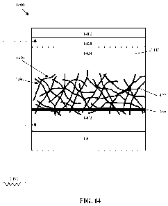
FIG. 14 is a schematic view of an exemplary photovoltaic device which includes
an absorption layer with a mesh of semiconducting carbon nanotubes embedded
therein,
the interface of the absorption layer and semiconducting carbon nanotubes
forming a
junction; and
CA 02736450 2011-03-07
WO 2010/030511 PCT/US2009/055143
-18-
FIG. 15 is a schematic view of an exemplary photodetector device coupled to a
voltage source for biasing thereof.
DETAILED DESCRIPTION
Certain exemplary embodiments will now be described to provide an overall
understanding of the principles of the structure, function, manufacture, and
use of the
devices and methods disclosed herein. One or more examples of these
embodiments are
illustrated in the accompanying drawings. The devices and methods specifically
described herein and illustrated in the accompanying drawings are non-limiting
exemplary embodiments, as the scope of the present application is defined
solely by the
claims. Throughout this application, the term "e.g." will be used as an
abbreviation of
the non-limiting phrase "for example."
A variety of embodiments will be presented herein. It should be understood
that
the features illustrated or described in connection with one exemplary
embodiment may
be combined with the features of other embodiments. Such modifications and
variations
are intended to be included within the scope of the present disclosure.
Generally, the devices and methods disclosed herein provide improved
photovoltaic cells for converting light, including in particular sunlight, to
electrical
energy. It should be understood that the terms "light" and "radiation" are
used
interchangeably herein to refer to both visible and invisible radiation. These
devices and
methods have a wide range of applications, including in both terrestrial and
extra-
terrestrial settings, and can be incorporated into panels, arrays, flexible
films, sheets, or
other products.
FIG. I schematically illustrates one embodiment of a photovoltaic device 100.
In this case, the photovoltaic device 100 includes a substrate 101, a back
electrical
contact 102, an absorption layer 104, a window layer 106, a top electrical
contact 108,
and an anti-reflective coating 110.
Typically, the absorption layer 104 is a light-responsive layer - that is, it
is
capable of generating electron-hole pairs in response to light of suitable
wavelengths
incident thereon. The bulk of the absorption layer 104 can be formed from a
semiconductor material 112. The bulk of the window layer 106 can also be made
of a
semiconductor material 114, and can also be light-responsive. In many
embodiments,
CA 02736450 2011-03-07
WO 2010/030511 PCT/US2009/055143
-19-
the semiconductor materials 112 and 114 are of differing conductivity types.
As is
known in the art, the conductivity type of a material refers to the type of
charge carrier
(e.g., electron or hole) that is predominantly responsible for electrical
conduction in the
material. The junction between two materials formed of different conductivity
types can
be characterized by a depletion region that supports an electric field, while
the junction
between two materials formed of similar conductivity types does not produce a
depletion
region. By way of example, the absorption layer 104 can be made of n-type CdSe
while
the window layer 106 can be made of p-type CdS, thus forming a p-n junction
130. As
is well known in the art, a p-n junction can have certain characteristics,
including the
aforementioned depletion region, an electric field and built-in voltage, all
of which
follow from the chosen semiconductor materials and doping profiles, among
other
things. As one skilled in the art will understand, a variety of semiconductors
(e.g.,
Group II-VI, Group IV, or Group III-V) and dopants can be used. In some
embodiments, the junction 130 can be a p-i-n junction that is formed by the
junction of a
p-type material, an intrinsic layer (e.g., an undoped or lightly doped
semiconductor
material), and an n-type material.
In FIG. 1, the absorption layer 104 has a plurality of nanostructures embedded
therein. In this embodiment, the nanostructures are carbon nanotubes 122,
although a
wide variety of carbonaceous or other nanostructures can be used. The term
nanostructure is used herein to refer to a material structure having a size in
at least one
dimension (e.g., a diameter of a tube, or a length, width or thickness of
another structure
such as a graphene sheet) that is less than about 1 micron, in other
embodiments less
than about 500 nm, about 100 nm, about 20 nm or about 1 rim. As shown, the
plurality
of carbon nanotubes 122 form a mesh 124, which can be made up of many
intertwined
and/or interconnected carbon nanotubes 122. For descriptive purposes, the mesh
124
can be said to have an aspect ratio defined by a height 126 taken in a
direction
substantially normal to the substrate surface 101' (a vertical direction 162
in FIG. 1) and
a width taken in a direction substantially parallel to the substrate surface
101' (a
horizontal direction 160 in FIG. 1). The carbon nanotubes 122 can be randomly
distributed across their width 128. In some cases, the carbon nanotubes 122 in
the mesh
can be substantially horizontally oriented (as shown in FIG. 1) such that the
nanotubes
predominantly extend farther in horizontal direction 160 than in vertical
direction 162,
CA 02736450 2011-03-07
WO 2010/030511 PCT/US2009/055143
-20-
although this is not necessary. The individual nanotubes 122 in the mesh 124
can be in
contact (e.g., ohmic contact) with other nanotubes 122 along a portion of
their surfaces,
creating a network of interconnected nanotubes 122. Ohmic contact is known in
the art;
however, to the extent that any additional explanation is necessary, ohmic
contact refers
to contact that allows exchange of charge carriers therebetween (e.g., a flow
of
electrons) and is characterized by a substantially voltage independent
resistance. In
many embodiments, the mesh 124 can provide a network of conductive pathways
within
the absorption layer 104.
Although the mesh 124 is illustrated as an arrangement of carbon nanotubes 122
without a discernible pattern, in other embodiments an organized mesh, e.g., a
patterned
mesh, can be used. In addition to whatever other characteristics (e.g.,
electrical
conductivity) it may provide, such a mesh can be used as a physical template
or screen
for the fabrication of layers, semiconductor nanostructures, or other features
in the
device 100, as will be discussed in more detail below.
The density of the mesh 124 can vary widely. However, in some embodiments,
the density of the carbon nanotubes 122 of the mesh 124 can be adjusted such
that the
interstitial spacing between neighboring nanotubes produces desirable
properties. For
example, as shown in FIG. 2, the spacing 200 between adjacent carbon nanotubes
122 in
the mesh 124 can be less than about three diffusion lengths exhibited by photo-
generated
minority charge carriers (e.g., upon photo-excitation) in the semiconductor
material 112
in which the mesh 124 is embedded, and more preferably less than about two
diffusion
lengths. It should be understood that while FIG. 2 is a two-dimensional
illustration, in a
three-dimensional device the interstitial spacing 200 can represent the
distance across
three-dimensional voids separating carbon nanotubes 122 in the mesh 124.
As shown in FIG. 1, the carbon nanotubes 122 in the mesh 124 can be coated
with the semiconductor material 112. In many cases, the semiconductor material
112
conformally coats individual nanotubes 122 in the mesh 124. A conformal
coating can
take the shape of the contours and/or underlying three-dimensional profile of
the carbon
nanotubes 122, and in some cases can cover surfaces of the carbon nanotubes
122 in
many or substantially all directions, e.g., in the nature of a circumferential
coating. In
some embodiments, the coating can at least partially cover at least about 5
percent of the
nanotubes 122 (or other nanostructures) in the material; in other embodiments,
between
CA 02736450 2011-03-07
WO 2010/030511 PCT/US2009/055143
-21 -
and 100 percent of individual nanotubes are at least partially coated. More
narrow
ranges are possible. For example, the coating can at least partially cover 5
and 10
percent of carbon nanotubes, between 5 and 20 percent, between 5 and 30
percent, about
5 40 percent, about 50 percent, about 75 percent, and so on.
The semiconductor material 112 can also fill in the spaces between carbon
nanotubes 122, such as the spaces 200 and/or three-dimensional voids discussed
above
in connection with FIG. 2. In FIG. 1, the semiconductor material 112 coating
on the
carbon nanotubes 122 has been built up such that it covers the mesh 124. In a
three
dimensional device, the junction 130 can be substantially planar. However, in
other
embodiments, the semiconductor material 112 can coat the nanotubes 122 without
being
built up, and a window layer can be disposed on top of the coated nanotubes
122 to
create a non-planar junction, as will be discussed in more detail below in
connection
with FIG. 3.
The semiconductor material 112 coating the carbon nanotubes 122 can be
crystalline, including both single-crystal and/or polycrystalline coatings,
and e.g.,
hexagonal phase crystalline CdSe. In some cases, a region of crystalline
material (e.g.,
single crystal) can surround the carbon nanotubes and/or each individual
carbon
nanotube. In some cases, other regions (e.g., regions beyond this surrounding
crystalline
region) can be polycrystalline or amorphous. However, in other embodiments, a
substantial portion of the bulk of the absorption layer 104 can be crystalline
(e.g., 80%
or more). Crystalline regions can have advantageous electrical properties,
e.g., they can
promote high-efficiency current generation and collection in the absorption
layer 104.
In many embodiments, the foregoing semiconductor materials and coatings can be
fabricated using chemical bath deposition (CBD) procedures, which will be
described in
more detail below.
The carbon nanotubes 122 can be coupled to the back electrical contact 102,
e.g.,
electrostatically or via an adhesive material, such that the carbon nanotubes
102 form a
contact (e.g., an ohmic contact) to the back electrical contact 102. The back
electrical
contact 102 (and/or substrate 101) can have a roughened or textured top
surface so as to
improve the anchoring of the carbon nanotubes 122 thereto. By way of example,
the top
surface can include micron or sub-micron sized undulations or can be a porous
surface,
CA 02736450 2011-03-07
WO 2010/030511 PCT/US2009/055143
-22-
e.g., with micron or sub-micron sized pores. Such a textured or roughened
surface can
be created using a variety of techniques, as will be described in more detail
below.
In many cases, the back electrical contact 102 is formed from an electrically
conductive material. It can be rigid or flexible, transparent or opaque. For
example, the
electrical contact 102 can be a film of electrically conducting material
(e.g., a metal such
as aluminum or copper) disposed atop a substrate 101, which itself can be
rigid (e.g., a
glass substrate) or flexible (e.g., plastic). The back electrical contact 102
can also take
the form of trace connections atop (e.g., patterned and deposited metals) or
through the
substrate 101 (e.g., drilled through the substrate 101). Further, in some
embodiments,
the back electrical contact 102 and the substrate 101 can be combined, as they
need not
be separate components or materials. The use of flexible electrical contacts
102 and/or
substrates 101 can be advantageous for producing flexible photovoltaic films.
The
flexibility of such films, and of such electrical contacts 102 and/or
substrates 101, can be
such that the film can be rolled and unrolled, e.g., for transport, storage,
and installation.
In some embodiments, the flexibility of the back electrical contact 102 and/or
substrate
101 can be such that will allow them to be rolled around and unrolled from a 1
inch
diameter cylinder repeatedly without damage.
Returning to FIG. 1, a top electrical contact 108 can be disposed over the
window layer 106. The top electrical contact 108 can be a layer formed from a
transparent conductive polymer (TCP), metal oxide, or polyimide, or can have
any of a
wide variety of other configurations, including an arrangement of fine metal
lines as is
known in the art. In many embodiments, the top contact can be radiation-
transparent
(for example, transparent to solar radiation, which can include radiation
having a
wavelength in a range of about 200 nm to 2.5 microns). The top electrical
contact 108
also can be configured as previously described with respect to the back
electrical contact
102. An anti-reflective coating 110, such as a silicon oxynitride thin film,
can be
disposed over the window layer 106 and the top electrical contact 108. The
photovoltaic
device 100 can be coated with or encapsulated in a protective material (e.g.,
to provide
physical and/or environmental protection), such as a transparent polymer or
PTFE. The
anti-reflective coating 110 and protective material are typically radiation-
transparent.
CA 02736450 2011-03-07
WO 2010/030511 PCT/US2009/055143
-23-
In use, and without being limited by theory, the device 100 can be exposed to
solar radiation that passes through the top electrical contact 108 without any
substantial
absorption to reach the window layer 106. Some of the photons passing through
the
window layer 106 can be absorbed by the semiconductor material 114 of that
layer to
generate electron-hole pairs. Other incident photons pass through that layer
106 to be
absorbed by the semiconductor material 112 of the absorption layer 104 so as
to
generate electron-hole pairs therein. The generation of electron-hole pairs
occurs, e.g.,
by promoting an electron in the valence band of the material to its conduction
band. As
previously mentioned, and for explanatory purposes only, the absorption layer
104 can
be made of n-type semiconductor (e.g., CdSe), while the window layer can be
made of
p-type semiconductor (e.g., doped CdS). In such an embodiment, the electric
field in the
junction 130 causes the separation of such electron-hole pairs in the vicinity
thereof.
Electrons can travel across the junction 130 to the n-type semiconductor and
the holes
can travel across the junction 130 to the p-type semiconductor. Additionally,
electron-
hole pairs are photo-generated outside the vicinity of the depletion region in
both the
absorption layer 104 and window layer 106. Such electrons and holes can move
(e.g.,
diffuse, as dictated by factors such as carrier concentration and thermal
effects in the
semiconductor) within the absorption layer 104 and window layer 106, as the
case may
be. This movement can be quantitatively described by their diffusion lengths
(e.g.,
average distance traveled by a charge carrier before recombination).
Whether generated inside or outside the vicinity of the junction 130,
photogenerated electrons can migrate (e.g, via diffusion) through the n-type
absorption
layer 104 to the carbon nanotubes 122 of the mesh 124 (e.g., before
recombining). The
carbon nanotubes 122 can provide a conductive pathway out of the absorption
layer 104
to the back electrical contact 102, which can reduce the chances that an
electron will
recombine with a hole before it can exit the absorption layer 104. (In this
embodiment,
electrons can also pass directly from the absorption layer 104 to the back
electrical
contact 102.) The removal of electrons can also reduce the recombination rate
for holes
in the absorption layer 104 by reducing the number of electrons with which
they can
recombine, which enhances the probability of reaching the depletion region of
the
junction 130 and the p-type window layer 106. Photogenerated holes can migrate
through the p-type window layer 106 to the top electrical contact 108. The
electrons in
CA 02736450 2011-03-07
WO 2010/030511 PCT/US2009/055143
-24-
the back electrical contact 102 can travel through an external load 150 to the
p-type
window layer 106 to recombine with the holes that have migrated through the
window
layer 106. This flow of electrons represents a current which, in conjunction
with the
built-in potential of the junction 130, represents electrical power.
As one skilled in the art will understand, in other embodiments the absorption
layer 104 can be made of p-type material, while the window layer can be made
of n-type
material, and the operation of such a device will change accordingly. In such
an
embodiment, photo-generated electrons in the window layer 106 travel to the
top
electrical contact 108, through an external load 150, and through the back
electrical
contact 102 and the carbon nanotubes 122 to recombine with holes in the p-type
absorption layer 104.
Without being limited by theory, in many cases, the mesh 124 of carbon
nanotubes 122 (or other carbon nanostructures) in the photovoltaic device 100
can
provide a conductive pathway and thereby reduce recombination of generated
electron-
hole pairs in the absorption layer 104, for example, by allowing free
electrons a low-
resistance path out of the absorption layer 104 to the back electrical contact
104.
Further, as noted above, in many embodiments, the density of the carbon
nanotubes 122
forming the mesh 124 is sufficient to ensure that a charge carrier (e.g., an
electron)
generated in the interstitial space between the carbon nanotubes 122 is likely
to reach a
carbon nanotube 122 before recombining (e.g., with a hole) or undergoing other
absorption and/or scattering event that would prevent them from flowing out of
the
absorption layer 104 to the external load 150. Use of carbon nanotubes 122 can
enable a
relatively thick absorption layer (which can be advantageous, e.g., for
absorbing a
greater proportion of incident radiation) to have the same or a lower electron-
hole
recombination rate as a relatively thin absorption layer (which can be
advantageous to
enhance efficiency of the device). In short, the device 100 can have the
advantages of a
thick absorbing layer with the lower recombination rate of a thin absorbing
layer.
A wide variety of materials can be used in the photovoltaic device 100. As
previously mentioned, the absorption layer 104 and window layer 106 can be
formed
from semiconductor materials 112, 114, including both single-element or
compound
semiconductors. Typically, the absorption layer 104 and window layer 106 can
have
differing conductivity types so that the junction therebetween can form a
depletion
CA 02736450 2011-03-07
WO 2010/030511 PCT/US2009/055143
-25-
region. Solely by way of non-limiting example, some potential Group II-VI
semiconductors which can be used for the layers 104, 106 include CdSe, CdS,
CdO,
ZnS, CdTe, ZnO, ZnSe, CuSe, and ZnTe. Group IV and III-IV semiconductors, or
other
semiconducting materials, also can be used. In addition, in some embodiments,
alternative materials can be substituted for the Group II material in a
nominally Group
II-VI compound semiconductor, e.g., a Group 1-111-VI semiconductor. For
example,
Copper Indium di-Selenide (CuInSe2) can be used, with the Copper Indium
compound
substituting for Cadmium (Group II) in its pairing with Selenium (Group VI) to
create a
Group I-III-VI semiconductor. The absorption and windows layers 104, 106 can
include
different semiconductor materials (e.g., n-type CdSe for the semiconductor
material 112
in the absorption layer 104 and p-type CdS, CuSe, or ZnTe for the
semiconductor
material 114 in the window layer 106, or vice versa). In other embodiments,
the
absorption and windows layers 104, 106 can include the same semiconductor
material,
doped to be of differing conductivities (e.g., n-type CdSe for the
semiconductor material
112 in the absorption layer 104 and p-type CdSe for the semiconductor material
114 in
the window layer 106, or vice versa). As one skilled in the art will
understand, the
chosen semiconductor materials and dopants can vary. Typically, some Group II-
VI
materials are intrinsically n-type (that is, without doping), such as CdSe and
CdS.
Others typically are intrinsically p-type (that is, without doping), such as
CdTe and
ZnTe. Such materials need not be doped; however, in many embodiments dopants
such
as Cu can be used as a p-type dopant (e.g., to change CdSe to a p-type
material via
appropriate dosages).
The thickness of the absorption layer 104 and window layer 106 can vary widely
and be designed to achieve suitable absorption of incident radiation. However,
in one
embodiment, the absorption layer 104 can have a thickness in a range of about
100 nm
to 10 microns, and more preferably each can have a thickness in a range of
about 300
nm to 3000 nm. The window layer 106 can have a thickness in a range of about
10 nm
tolO,000 nm, and preferably 50 to 2000 nm, and more preferably about 50 nm to
500
nm. Referring to FIG. 1, the mesh 124 of carbon nanotubes 122 embedded in the
absorption layer 104 can extend virtually to any height 126 within the layer.
A region
132 of the absorption layer, preferably adjacent the junction 130, can be
substantially
devoid of nanostructures. Although the region 132 devoid of nanostructures can
have
CA 02736450 2011-03-07
WO 2010/030511 PCT/US2009/055143
-26-
virtually any thickness, it is preferably thicker than the depletion region of
the junction
130 within the absorption layer 104. Further, while it is not necessary, the
region 132
preferably can have a thickness that is less than about three, or in some
cases about two,
diffusion lengths of photo-generated minority carriers in the semiconductor
material
included in the second layer. For example, in one embodiment the mesh 124 of
carbon
nanostructures 122 can extend to a height 162 of about 500 nm within the
absorption
layer 104, and a region 132 devoid of nanostructures can be about 500 nm
thick, which
can result in an overall absorption layer 104 thickness of about 1000 nm.
However, all
such dimensions are merely by way of illustration and can vary widely.
It should be understood that while FIG. 1 is shown with an absorption layer
104
and window 106, multiple layers can be included. For example, additional
absorption
layers and/or window layers can be disposed above the window layer 106 (or in
other
embodiments, below the absorption layer 104) to form a multiple-junction
device. Such
additional layers can include nanostructures such as carbon nanotubes 122
embedded
therein, but need not do so.
As previously mentioned, the nanostructures shown in FIG. 1 can be a mesh 124
of carbon nanotubes 122, which can be multi-wall carbon nanotubes or single-
wall
carbon nanotubes. A wide variety of other nanostructures (both carbon and non-
carbon)
also can be used, including cylindrical, spherical, elongate, ovoid, oblate,
and other
shapes, as well as carbon nanostructures formed from C60 molecules, C72
molecules, C84
molecules, C96 molecules, C108 molecules, or C120 molecules. In many
embodiments,
carbon nanostructures are formed primarily of carbon atoms (e.g., carbon can
constitute
90% or more of a nanostructure's composition). However, they can include other
constituents, for example, a plurality of catalyzing iron atoms from carbon
nanostructure
fabrication. In some embodiments, the nanostructures can include graphene
structures.
For example, the mesh 124 can comprise a mesh of one more graphene structures.
Typical graphene structures are planar sheets or platelets with a thickness of
one-atom.
The length and width of such graphene structures can vary widely, but in one
embodiment they can have a width of about 150 nm and a length of about 100 nm
to
about 1000 nm.
CA 02736450 2011-03-07
WO 2010/030511 PCT/US2009/055143
-27-
The fabrication of carbon nanostructures, including single and multi-wall
carbon
nanotubes, is known in the art. By way of example, carbon nanotubes can be
fabricated
using a variety of techniques, including chemical vapor deposition, laser-
ablation, and
arc discharge. Methods of fabricating carbon nanotubes are disclosed in more
detail in
U.S. Patent Nos. 7,125,534 (Smalley et al., "Catalytic growth of single- and
double-wall
carbon nanotubes from metal particles"), 7,150,864 (Smalley et al., "Ropes
comprised of
single-walled and double-walled carbon nanotubes") and 7,354,563, (Smalley et
al.,
"Method for purification of as-produced fullerene nanotubes"), which are
hereby
incorporated by reference in their entirety. Further, suitable carbon
nanostructures can
be obtained from commercial suppliers, such as Nanocyl of Sambreville, Belgium
(US
office in Rockland, MA, USA), Bayer Materials Science AG of Leverkusen,
Germany,
and Showa Denko K.K. of Japan. Graphene can be fabricated according to known
techniques. One such techniques involves unrolling a carbon nanotube (e.g., a
multiwalled carbon nanotube) to create a graphene sheet. Other techniques are
described, for example, in U.S. Patent Publication No. 2008/0279756 (Zhamu et
al.,
"Method of producing exfoliated graphite, flexible graphite, and nano-scaled
graphene
platelets," discussing a method of fabricating graphene that involves a)
dispersing
particles of graphite, graphite oxide, or a non-graphite laminar compound in a
liquid
medium containing therein a surfactant or dispersing agent to obtain a stable
suspension
or slurry; and (b) exposing the suspension or slurry to ultrasonic waves at an
energy
level for a sufficient length of time to produce separated nano-scaled
platelets); and in
U.S. Patent Publication No. 2009/0200707 (Kivioja et al., "METHOD OF
FABRICATING GRAPHENE STRUCTURES ON SUBSTRATES," discussing a
method of fabricating graphene that involves stamping or pressing a body of
graphite
against a substrate), all of which are hereby incorporated by reference.
In many cases, the nanostructures are more conductive than the surrounding
material in the absorption layer 104. The nanostructures can advantageously
have a
band gap less than that of the material forming the bulk absorption layer 104
and
preferably a vanishing band gap. For example, the nanostructures can have a
band gap
of 0.1 eV or lower, and preferably 0.01 eV or lower. The band gaps of some
single-wall
carbon nanotubes have been measured to be about 0.6eV, and the band gaps (Eg)
of
CA 02736450 2011-03-07
WO 2010/030511 PCT/US2009/055143
-28-
some multi-wall carbon nanotubes can be calculated using Eg = 0.6/d where d is
the
outer diameter of the multi-wall carbon nanotube in nanometers, as is known in
the art.
In some embodiments, it can be advantageous for the carbon nanotubes 122 or
other nanostructures to be formed of a material having an index of refraction
less than
that of the material forming the bulk of the absorption layer 104. Light
traveling
through the absorption layer 104 can be internally reflected within the
semiconductor
material 112 at the interfaces between the carbon nanotubes 122 and the
semiconductor
material 112, increasing the opportunity for photons to be absorbed by the
layer 104 and
to generate electron-hole pairs. For example, the index of refraction for some
carbon
nanotubes has been measured to be about 2, while the index of refraction of
CdSe has
been measured to be about 2.6.
In one embodiment of a method for fabricating the above-described photovoltaic
device 100, carbon nanotubes can be deposited onto an electrical contact 102
and/or
substrate 101. As previously mentioned, the back electrical contact 102 and/or
substrate
101 can be roughened or textured, which can be accomplished, for example, via
mechanical abrasion or chemical etching. The carbon nanotubes 102 can be
deposited
via any of a variety of suitable techniques, such as a Langmuir-Blodgett
process, spin
coating, inkjet printing, or spraying. The density of the carbon nanotubes 122
can be
controlled by adjusting the amount deposited in an area. In other embodiments,
buckypaper or other commercially available nanotube sheets or films (e.g, pre-
formed)
can be used. Such sheets are available, for example, from Nanocomp
Technologies, of
Concord, NH, USA. To create an absorption layer 104, the semiconductor
material 112,
such as CdSe, can be grown on the carbon nanotubes 122 using a chemical bath
deposition (CBD) technique. Typically, a CBD reaction involves preparing
aqueous or
non-aqueous solutions containing appropriate precursor compounds (for example,
Cadmium precursor solution and Selenium precursor solution) and appropriate
ligands.
Aliquots of these solutions can be combined in a CBD container, and the object
(e.g.,
carbon nanostructure, wafer, or otherwise) onto which the film will be
deposited can be
immersed in the resulting chemical bath. The object remains immersed for the
time
required to form a film of the desired thickness. After removal, the object(s)
are rinsed
to remove excess reactants and dried for use. It should be understood that the
foregoing
is a general description and by way of illustration only. CBD processes are
described in
CA 02736450 2011-03-07
WO 2010/030511 PCT/US2009/055143
-29-
more detail in U.S. Patent No. 7,253,014 (Barron et al., "Fabrication Of Light
Emitting
Film Coated Fullerenes And Their Application For In-Vivo Light Emission"), and
in
U.S. Patent Publication No. 2005/0089684 (Barron et al., "Coated Fullerenes,
Composites And Dielectrics Made Therefrom"), both of which are hereby
incorporated
by reference in their entirety.
The thickness of the semiconductor coating on the carbon nanotubes 122 can be
grown so as to fill in the interstices between carbon nanotubes 122 in the
mesh 124, and
can be built up above the mesh 124, e.g., to cover the carbon nanotubes 122
and to form
a uniform surface for a planar junction 130, as shown in FIG. 1.
The CBD process can provide a crystalline semiconductor coating (including a
CdSe crystalline coating having a hexagonal phase) on the carbon nanotubes
122. For
example, the crystalline coating can be a single crystal and/or have
crystalline regions
formed therein. In some cases, the carbon nanotubes 122 can promote the growth
of
crystalline regions in the semiconductor material 112, for example by
nucleating growth
of the semiconductor material 112 on the carbon nanotube surfaces. As
previously
mentioned, the crystalline regions can have advantageous electrical
properties, e.g., they
can promote high-efficient current generation and collection in the absorption
layer 104.
In some embodiments, the deposited semiconductor material 112 can be annealed
to
facilitate the production of a coating of crystalline material. By way of
example, such
annealing can be performed at an elevated temperature (e.g., in a range of
about 300 -
1000 degrees Celsius) and for a suitable duration (e.g., a few second to a few
hours).
In some embodiments, the window layer 106 can be deposited on the absorption
layer 104 via CBD (e.g., via another bath deposition again using CBD
techniques). The
top electrical contact 108 can be fused into place with another CBD bath or
deposited
directly with CBD.
The foregoing is by way of example only, and a range of variations are
possible
and are intended to be within the scope of this disclosure. For example, the
carbon
nanotubes 122 can be coated with the semiconductor material 112 (to act, for
example,
as a seed layer) before being deposited onto the back electrical contact
102/substrate
101. In such an embodiment, another CBD bath can be performed after the carbon
nanotubes 122 are deposited to increase the thickness of the coating of the
semiconductor material 112. Further, in other embodiments, other processes for
CA 02736450 2011-03-07
WO 2010/030511 PCT/US2009/055143
-30-
depositing the semiconductor materials and/or other layers of the photovoltaic
device
can be used, including chemical vapor deposition, molecular beam epitaxy,
atomic layer
deposition, and electrochemical deposition.
A variety of other embodiments of photovoltaic devices and methods are
presented below; however it should be understood that any of them can employ
any of
the features already described in connection with FIGS. 1-2 (including, for
example, the
materials, fabrication processes, dimensions, and so on), as they are intended
to build on
the foregoing discussion.
FIG. 3 illustrates another embodiment of a photovoltaic device 300. In this
embodiment, the photovoltaic device 300 has an absorption layer 304 that
includes a
light-responsive material (here, semiconductor material 312) conformally
coating a
mesh 324 of carbon nanotubes 322. A window layer 306, which can be made of
semiconductor material 314 and as previously mentioned can also be light-
responsive, is
disposed on the absorption layer 304 to form a junctions 330 at the interfaces
of the two
layers. Although here the window layer 306 has been built up to a uniform
surface, it
need not be so (for example, alternatively the front electrical contact 308
can be a
transparent conductor (e.g., a doped metal oxide) deposited on the window
layer 306 and
built up to a uniform level). The mesh 324 shown in FIG. 3 extends out of the
absorption layer 304 and through an insulating layer 336 to an electrical
contact 302,
which is disposed on a substrate 301. The insulating layer 336, which can be
made for
example of silicon dioxide, can be provided between the back electrical
contact 302 and
the absorption layer 304 to prevent a short circuit path around the junction
330. In
addition, a top electrical contact 308 and an anti-reflective coating 310 can
be disposed
on top of the window layer 306. These and other aspects of the photovoltaic
device 300
can be as described in connection with the photovoltaic devices of previous
Figures.
The photovoltaic device 300 shown in FIG. 3 can be fabricated using the
techniques described above in connection with FIG. 1, with some adjustments.
For
example, instead of building up the absorption layer 104 by filling in the
interstitial
spaces between the coated carbon nanotubes to form a planar junction 130, the
CBD
process can be used (for example, by controlling bath concentrations and
immersion
times used with the CBD bath) to create a conformal coating on the carbon
nanotubes
322 that does not necessarily fill up the interstitial spaces. In some cases,
the thickness
CA 02736450 2011-03-07
WO 2010/030511 PCT/US2009/055143
-31 -
of the semiconductor coating can be in a range of about 10 nm to 1000 nm. The
window
layer 306 can be deposited onto the absorption layer 304 via CBD.
FIG. 4 illustrates another embodiment of a photovoltaic device 400 that
includes
a substrate 401, a back electrical contact 402, an absorption layer 404, a
window layer
406, a top contact 408, and an anti-reflective coating 410. In this
embodiment, the
absorption layer 404 and the back electrical contact 402 are separated by a
gap 450. As
shown, the gap 450 is open, although in some embodiments it can be filled with
a
material (e.g., an insulating material). The mesh 424 of carbon nanotubes 422
can
extend out of the absorption layer 404 to the back electrical contact 402 to
form a
contact (e.g., an ohmic contact) therewith. The portion of the mesh 424 that
spans the
gap 450 can include uncoated carbon nanotubes 422. In some embodiments, the
size of
the gap 450 (e.g., the size across the gap from the absorption layer 404 to
the back
electrical contact 402) can be in a range of about 100 nm to 10,000 nm; or
more
preferably in a range of about 500 nm to 1,000 nm. Other aspects of the
photovoltaic
device 400 can be as described in connection with the photovoltaic devices of
previous
Figures. In some embodiments, the photovoltaic device 400 can include two
meshes of
carbon nanostructures, one of which is at least partially disposed in the
absorption layer
404 and the other of which is attached to the back electrical contact 402, the
two meshes
being electrically connected.
The photovoltaic device 400 shown in FIG. 4 can be fabricated using the
techniques described above in connection with FIG. 1, with some adjustments.
For
example, the CBD process can be used to partially coat the carbon nanotubes
422 with a
semiconductor material 412. These partially coated nanotubes can be deposited
on the
back electrical contact 402 to create a mesh 424, leaving the portion of the
mesh 424
closest to the back electrical contact 402 substantially uncoated. The
absorption layer
404 can be formed by filling in the interstitial spaces of the mesh 424. In
some
embodiments, the mesh 424 of carbon nanotubes 422 can be coated with a
semiconductor material 412 (e.g., via CBD or other process), and then etched
on the
bottom surface to remove some of the deposited material. The partially coated
nanotubes 122 can then be disposed on the back electrical contact 402.
CA 02736450 2011-03-07
WO 2010/030511 PCT/US2009/055143
-32-
Although the foregoing embodiments have illustrated a mesh of carbon
nanotubes, a variety of other configurations are possible. FIG. 5 shows an
exemplary
photovoltaic device 500 with an absorption layer 504 that includes a "carpet"
of aligned
nanostructures, e.g., substantially vertically oriented nanostructures, which
in this
embodiment are carbon nanotubes 522. As used herein, substantially vertically
oriented
means that the nanotubes are nearly, but not exactly, normal to the substrate
501. In
many embodiments, the nanotubes can be substantially vertically oriented such
that the
angle between the nanostructure (e.g., along its height 526) and a vector 562
that is
normal to the substrate surface 501' is less than about 45 degrees. In some
cases, the
orientation of the embedded carbon nanotubes 522 can be such that the majority
of
nanotubes extend farther in a direction substantially normal to the surface
501' of the
substrate 501 (a vertical direction 562 in FIG. 5) that is greater than they
extend in a
direction substantially parallel to the surface 501' of the substrate 501 (a
horizontal
direction 560 in FIG. 5), although this is not necessary. In some cases, the
carbon
nanotubes 522 are upstanding (e.g., the carbon nanotubes can have a sidewall
522a and
an end cap 522b, and they can be substantially supported on the substrate by
the end cap
522b).
The carpet of carbon nanotubes 522 can be arranged in a wide variety of ways.
In FIG. 5, the carbon nanotubes 522 are spaced at substantially regular
intervals from
one another. However, in other embodiments, the spacing need not be regular.
Further,
the carbon nanotubes 522 can be placed in bunches, such bunches being spaced
apart
from one another. As previously mentioned, it can be advantageous to arrange
the
spacing 580 between adjacent carbon nanotubes 522 to be less than about three
diffusion
lengths exhibited by photo-generated minority charge carriers (e.g., upon
photo-
excitation) in the semiconductor material 512 incorporated therebetween, and
more
preferably less than about two diffusion lengths. It should be understood that
while FIG.
5 is a two-dimensional illustration, in a three-dimensional device the
interstitial spacing
580 can represent the distance across three-dimensional voids separating
carbon
nanotubes 522.
The carbon nanotubes 522 can have virtually any size, but preferably they do
not
extend into the junction 530. For example, the carbon nanotubes 522 can have a
height
of about 200 nm to 5000 nm and can be embedded in an absorption layer 504 that
is
CA 02736450 2011-03-07
WO 2010/030511 PCT/US2009/055143
-33-
about 3 diffusion lengths thicker than the nanotubes are tall (for example,
the nanotubes
can be about 500 nm) in a region about 1000 nm thick, leaving a region 532
devoid of
about 500 nm devoid of nanostructures. However, all such dimensions are merely
by
way of illustration and can vary widely.
As shown, a semiconductor material 512 which forms the bulk of the absorption
layer 504 conformally coats the individual carbon nanotubes 522, filling in
the spaces in
between them and embedding them in the absorption layer 504. The material 512
can
have crystalline regions 570 therein, which can be as previously described. A
window
layer 506 can be disposed over the absorption layer 504 and can be made of a
semiconductor material 514, with the interface of the absorption layer 504 and
window
layer 506 creating a junction 530 with a depletion region.
The photovoltaic device 500 can also include a substrate 501, a back
electrical
contact 502, a top electrical contact 508, and an anti-reflective coating 510.
These and
other aspects of the photovoltaic device 500 can be as described in connection
with the
photovoltaic devices of previous Figures.
Operation of the photovoltaic device 500 with upstanding carbon nanotubes 522
can be similar to that of the photovoltaic device 100 in many respects.
Photons incident
on the photovoltaic device 500 can generate electron-hole pairs in the
absorption layer
504 and/or in the window layer 506. As previously mentioned, and for
explanatory
purposes only, the absorption layer 504 can be made of an n-type semiconductor
(e.g.,
CdSe), while the window layer can be made of a p-type semiconductor (e.g.,
doped
CdS). In such an embodiment, the electric field in the junction 530 causes the
separation
of such electron-hole pairs in the vicinity thereof. Such electrons can travel
across the
junction 530 to the n-type semiconductor and the holes can travel across the
junction
530 to the p-type semiconductor. Additionally, electron-hole pairs are photo-
generated
outside the vicinity of the depletion region in both the absorption layer 504
and window
layer 506. Such electrons and holes can move (e.g., diffuse) within the
absorption layer
504 and window layer 506.
Whether generated inside or outside the vicinity of the junction 530,
photogenerated electrons can migrate through the n-type absorption layer 504
to the
carbon nanotubes 522, which can provide a conductive pathway out of the
absorption
layer 504 to the back electrical contact 502, although in this embodiment
electrons can
CA 02736450 2011-03-07
WO 2010/030511 PCT/US2009/055143
-34-
also pass directly from the absorption layer 504 to the back electrical
contact 502.
Photogenerated holes can migrate through the p-type window layer 506 to the
top
electrical contact 508. The electrons in the back electrical contact 502 can
travel
through an external load 550 to the p-type window layer 506 to recombine with
the holes
that have migrated through the window layer 506.
The photovoltaic device 500 can be fabricated using the techniques described
above in connection with the photovoltaic device 100, with some adjustments.
For
example, the CBD process can be used to coat aligned (e.g., vertically
aligned) carbon
nanotubes 722 rather than the mesh 124 described in conjunction with
photovoltaic
device 100. The fabrication of aligned carbon nanotubes is known in the art
through a
variety of techniques. For example, aligned nanotubes can be grown chemical
vapor
deposition (CVD), such as plasma-enhanced hot filament chemical vapor
deposition
using acetylene as a carbon source and ammonia as a dilution and catalytic
agent, as
described in Huang et al., "Growth of highly oriented carbon nanotubes by
plasma-
enhanced hot filament chemical vapor deposition," Applied Physics Letters,
Vol. 73 No.
26, 3845 (1998), and Ren et al., "Synthesis of Large Arrays of Well-Aligned
Carbon
Nanotubes on Glass," Science 282, 1105 (1998), which are hereby incorporated
by
reference. Aligned nanotubes have been grown using CVD techniques on patterned
silicon substrates using Fe/Mo nanoparticles as catalysts and CO and H2 as
feed gases.
Such techniques are described in Huang et al., "Growth Mechanism of Oriented
Long
Single Walled Carbon Nanotubes Using `Fast-Heating' Chemical Vapor Deposition
Process," Nano Letters, Vol. 4, No. 6, 1025-1028 (2004), which is hereby
incorporated
by reference. Other alignment techniques include the use magnetic fields,
mechanical
shear, and gel extrusion, as discussed in Fischer et al., "Magnetically
aligned single wall
carbon nanotubes films: Preferred orientation and anisotropic properties,"
Journal of
Applied Physics, Vol. 93 No. 4, 2157 (2003), which is hereby incorporated by
reference.
Inkjet printing can be used in some circumstances. Further, arrays of carbon
nanotubes
can be commercially obtained from suppliers, as previously mentioned. More
details on
the formation and alignment of carbon nanotubes can be obtained with reference
to U.S.
Patent Publication Nos. 2005/0260120 (Smalley et al., "Method For Forming An
Array
Of Single-Wall Carbon Nanotubes In An Electric Field And Compositions
Thereof')
CA 02736450 2011-03-07
WO 2010/030511 PCT/US2009/055143
-35-
and 2005/0249656 (Smalley et al, "Method For Forming A Patterned Array Of
Single-
Wall Carbon Nanotubes").
In FIG. 5, the semiconductor material 512 has been built up to cover the tops
of
the carbon nanotubes 522 and create a substantially planar junction 522.
However, the
semiconductor material 512 (relative to that shown in FIG. 5) need not be so
thick. FIG.
6 illustrates such an alternate embodiment. FIG. 6 shows a photovoltaic device
600
which has semiconductor material 612 conformally coating individual carbon
nanotubes
622 in a carpet of substantially vertically oriented carbon nanotubes 622. A
window
layer 606, which is made of semiconductor material 614, is disposed on the
absorption
layer 604 to form a non-planar junction 630. The carbon nanotubes extend to an
electrical contact 602, which is disposed on substrate 601. In addition, a top
electrical
contact 608 and an anti-reflective coating 610 can be disposed on top of the
window
layer 606. These and other aspects of the photovoltaic device 600 can be as
described in
connection with the photovoltaic devices of previous Figures.
FIG. 7 illustrates another exemplary photovoltaic device 700 which includes a
light-responsive absorption layer 704 made of a semiconductor material 712 in
which
are embedded nanostructures (in this case carbon nanotubes 722) that are
conformally
coated with a film made of a semiconductor material. The absorption layer 704
and the
coating 706 can be doped to have differing conductivity types (e.g., n-type
and p-type)
so as to form a junction 730 at the interface of the coating of each carbon
nanotubes 722
and the semiconductor material 712 with a depletion region. In this manner,
the carbon
nanotubes 722 extend through a porous insulating layer 736, such as a silica
layer, which
separates the absorption layer 704 from the back contact 702 and substrate
701. A top
electrical contact 708 can be provided above the absorption layer 704, and an
anti-
reflective-layer 710 can be provided above the top electrical contact 708.
These and
other aspects of the photovoltaic device 700 can be as described in connection
with the
photovoltaic devices of previous Figures.
In use, photons incident on the photovoltaic device 700 can generate electron-
hole pairs in the semiconductor material 712 of the absorption layer 704 and
in the
semiconductor material of the coating 706. For explanatory purposes only, the
absorption layer 704 can be made of an n-type semiconductor, while the coating
706 can
be made of a p-type semiconductor. In such an embodiment, the electric field
in the
CA 02736450 2011-03-07
WO 2010/030511 PCT/US2009/055143
-36-
junction 730 causes the migration of holes through the p-type coating 706 to
carbon
nanotubes 722, which in turn provide an electrically conductive path to the
back
electrical contact 702. The electric field also causes the migration of
electrons through
the n-type absorption layer 704 to the top electrical contact 708. The
electrons travel
through an external load 750, through the back electrical contact 702 and the
carbon
nanotubes 722, and recombine with the holes in the p-type coating 706.
The photovoltaic device 700 can be fabricated using the techniques described
above in connection with the photovoltaic device 100, with some adjustments.
For
example, the coating 706 (e.g., semiconductor 714, such as p-type CdTe) can be
grown
on each individual carbon nanotube 722 (e.g., the carbon nanotubes can have a
sidewall
722a and an end cap 722b, and both sidewall 722a and endcap 722b can be
coated),
followed by a deposition of a seed layer of semiconductor material 712 (e.g.,
n-type
CdSe). The coated carbon nanotubes 722 can then be deposited on the back
electrical
contact 702, e.g., in a manner previously described. The absorption layer 704
can be
grown over the carbon nanotubes 722 (e.g., building up the thickness of
semiconductor
material 712) and the top electrical contact 708 can be fused thereon.
Other nanostructures can be incorporated into the exemplary photovoltaic
devices disclosed herein, including in particular semiconductor
nanostructures. Such
nanostructures may exhibit quantum effects, e.g., acting as quantum dots, or
may be
substantially free of quantum confinement effects.
FIGURE 8A schematically depicts an exemplary photovoltaic device 800
accordingly to another embodiment of the invention that includes absorption
layer 804
and window layer 806, which can be semiconductor light responsive layers, as
previously described. As shown, the absorption layer 804 and window layer 806
are in
contact with one another along a planar junction 830. By way of illustration,
in this
embodiment, the absorption layer 804 can be made of a semiconductor material
812
doped to be n-type while the window layer 806 can be made of a semiconductor
material
814 doped to be p-type. In other embodiments, the n- and p-type doping of the
layers
can be reversed.
A plurality of carbon nanostructures 822 (e.g., in this case, carbon
nanotubes,
which can be single-wall or multi-wall tubes) forming a mesh 824 are
distributed within
the absorption layer 804. As previously described, however, a portion of the
absorption
CA 02736450 2011-03-07
WO 2010/030511 PCT/US2009/055143
-37-
layer 804 in the vicinity of the junction 830 can remain substantially free of
such carbon
nanostructures 822 to ensure that the carbon nanostructures 822 do not provide
a
conductive path across the junction 830.
In this embodiment, the absorption and window layers 804, 806 are sandwiched
between two electrically conductive layers (shown as back electrical contact
802 and top
electrical contact 808) such that the absorption layer 804 forms a contact
(e.g., ohmic
contact) with the back electrical contact 802 and the window layer 806 forms a
contact
(e.g., ohmic contact) with the top electrical contact 808. The mesh 824 of
carbon
nanostructures is also in contact (e.g., ohmic contact) with the back
electrical contact
802 to provide an electrically conductive path out of the absorption layer 804
thereto.
The layer 810 can be formed of an antireflective and transparent material to
allow the
passage of photons incident thereon to the absorption and window layers 804,
806.
With continued reference to FIGURE 8A, a plurality of composite nanostructures
870 are disposed over (and in some cases, in between) the mesh 824 of carbon
nanostructures 822 so as to be in electrical contact therewith. In this
embodiment, the
composite nanostructures 870 include a core formed primarily of carbon and a
shell
formed of a semiconductor material. The semiconductor shell of the composite
nanostructures 870 can have the same conductivity type as that of the material
812
forming the bulk of the absorption layer 804 (e.g., both can include n-type
doping, such
as n-type/n-type or n+-type/n-type) to prevent the formation of a depletion
region at the
interface of the semiconductor shells and the material 812.
By way of illustration and with reference to FIGURE 8B, a composite
nanostructure 870 can include a core 870b formed of a carbon nanostructure and
a
semiconductor shell 870a. By way of example, the composite nanostructures 870
can be
in the form of substantially spherical particles having a carbon core with a
diameter, e.g.,
in a range of about 0.7 nm to about 100 nm, and a semiconductor shell 870a. In
many
embodiments, the thickness of the semiconductor shell 870a is selected such
that the
optical properties of the shell 870a (e.g., its band gap) are not dominated by
quantum
confinement effects. By way of example, the semiconductor shell 870a can have
a
thickness in a range of about 1 nm to about 100 nm, or in a range of about I
nm to about
50 nm, or in a range of about 1 nm to about 30 nm, or in a range of about 1 nm
to about
20 nm, or in a range of about 1 nm to about 10 nm. In other embodiments, the
CA 02736450 2011-03-07
WO 2010/030511 PCT/US2009/055143
-38-
semiconductor shells 870a of the nanocomposite structures 870 can provide
quantum
confinement (e.g., they can function as quantum dots). The semiconductor
material of
the shell 870a can advantageously be crystalline.
By way of example, in this embodiment, the core 870b can be formed of C60
molecules, C72 molecules, C84 molecules, C96 molecules, C108 molecules, or
C120
molecules, which are herein referred to as buckyballs, while in other
embodiments the
core 870b can be formed of a carbon nanotube (e.g., a single-wall or multi-
wall
nanotube). The semiconductor shell 870a can in turn be formed of any suitable
semiconductor material, such as Group 11-VI semiconductor materials. Although
in this
embodiment the semiconductor shell 870a is shown as completely coating the
core 870b,
in other embodiments the shell 870a can partially coat the core 870b such that
a portion
of the core remains exposed. In some cases, the uncoated portions of such
partially
coated cores can be in electrical contact with the carbon nanostructures 822
of the mesh
824 to facilitate the transfer of charge carriers generated in the
semiconductor shell 870b
(e.g., in response to absorption of a photon) to the mesh 824.
In many embodiments, the semiconductor shells can be formed of a
semiconductor material having a smaller band gap that that of the material
forming the
bulk of the absorption layer 804 so as to enhance the absorption of photons
passing
through that layer. It should also be understood that the composite
nanostructures 870
can be replaced by nanostructures without a composite structure (e.g., a
nanostructure
formed of a semiconductor material without a carbon core), which can also be
formed of
a semiconductor material having a smaller band gap that that of the material
forming the
bulk of the absorption layer 804.
In use, the conductive layer 808 can be exposed to solar radiation that passes
through that layer 808 without any substantial absorption to reach the window
layer 806.
Some of the photons passing through the window layer 806 can be absorbed by
the
material 814 of that layer to generate electron-hole pairs. Other incident
photons pass
through that layer 806 to be absorbed by the material 812 of the absorption
layer 804 so
as to generate electron-hole pairs therein. In some embodiments, the band gap
of the
material 814 forming the layer 806 is greater than the band gap of the
material 812
forming the bulk of the absorption layer 804. Further, as noted above, the
band gap of
the semiconductor material forming the shells 870b of the composite
nanostructures 870
CA 02736450 2011-03-07
WO 2010/030511 PCT/US2009/055143
-39-
can be less than that of the material 812 forming the bulk of the absorption
layer 804.
Such "cascading" of the band gaps can advantageously enhance the absorption of
photons by the photovoltaic cell 800 as the layer 804 can absorb, in addition
to high
energy photons, some of the lower energy photons to which layer 806 is
transparent due
to its larger band gap. Likewise, the semiconductor shells 870b can absorb
some of the
photons having energies less than that corresponding to the band gap of the
material 812
forming the bulk of the layer 804, although the shells 870b may also absorb
high energy
photons that were not absorbed (e.g., by the materials 812, 814 in the layers
804, 806)
before reaching the composite nanostructures 870.
The carbon nanostructures 822 can also produce light-trapping effects (e.g.,
by
providing an index of refraction less than that of the material 812 in the
bulk of the layer
804 so as to cause internal reflection therein), as described previously.
The absorbed photons can generate electron-hole pairs. As previously described
in connection with other embodiments, in the context of an n-type material 812
and p-
type material 814, electrons can migrate to the back electrical contact 802
via the carbon
nanostructures 822 (or directly). Holes can migrate to the front electrical
contact 808.
Electrons can pass through the load 850 and arrive at the front electrical
contact 808 and
the window layer 806 to recombine with the holes that have migrated within
that layer.
The photovoltaic device 800 shown in FIG. 8A can be fabricated using the
techniques described above in connection with FIG. 1, with some adjustments.
In some
embodiments, the composite nanostructures 870 can be fabricated by initially
forming
the carbon nanostructure cores 870b via any of a number of fabrication
techniques
known in the art, as previously mentioned. In some embodiments, the carbon
cores
870b can then be coated with a semiconductor shell 870a by utilizing CBD
techniques,
such as those previously discussed. The thickness of the semiconductor shell
870a can
be adjusted by allowing the chemical bath deposition to proceed for a selected
time
period. Alternatively, other techniques, such as atomic layer deposition,
molecular beam
epitaxy, or chemical vapor deposition, can be utilized to coat carbon cores
with a
semiconductor shell.
The use of a carbon core 870b as a "scaffolding" for the formation of the
semiconductor shell 870a can provide certain advantages. For example, it can
allow for
the generation of a plurality of nanoparticles whose sizes are narrowly
distributed. More
CA 02736450 2011-03-07
WO 2010/030511 PCT/US2009/055143
-40-
specifically, it can facilitate the formation of a semiconductor shell with a
desired
nanosized thickness, and consequently a desired band gap. For example, the use
of
bucky balls as the carbon cores allows the formation of a plurality of
substantially
spherical nanoparticles with a carbon core and semiconductor shell having
diameters
within a narrow distribution about an average diameter. The ability to
generate the
composite nanostructures 870 with substantially uniform sizes allows the
nanoparticles
to have substantially similar band gaps, e.g., in the above embodiment of FIG.
8A the
band gap value less than that of the bulk of the absorption layer 804.
As noted above, a variety of semiconductor materials can be utilized to form
the
semiconductor shell 870a, including any of the materials 812, 814 used in the
absorption
layers 804 and window layer 806, as detailed above in connection with FIG. 1.
By way
of example, in one embodiment the bulk of the absorption layer 804 is formed
of CdS
(e.g., with n-type or p-type doping), the window layer 806 is formed of ZnO,
and the
semiconductor shells 870a of the composite nanostructures 870 are formed,
e.g., of
CdSe or CdTe, having the same conductivity type as that of the bulk of the
absorption
layer 804.
Although FIG. 8A illustrates the incorporation of nanostructures 870 into a
photovoltaic device which has a mesh 824 of carbon nanostructures 822, in
other
embodiments, semiconductor nanostructures can be similarly incorporated into
photovoltaic devices with upstanding carbon nanostructures, such as the
photovoltaic
device shown in FIG. 5.
FIG. 9 illustrates another exemplary photovoltaic device 900, which has an
absorption layer 904 formed from a semiconductor material 912 (e.g., an n-type
semiconductor, such as n-type CdSe) and a window layer 906 formed from a
semiconductor material 914 (e.g., a p-type semiconductor, such as p-type doped
CdS).
As shown, the absorption layer 904 and window layer 906 form a junction 930
(e.g., a p-
n junction).
A plurality of carbon nanostructures (in this case, carbon nanotubes 922) are
embedded in the absorption layer 904. Semiconductor nanostructures 970 can be
disposed on portions of the outer surfaces of the carbon nanotubes 922. The
semiconductor nanostructures 970 can be made (e.g., entirely or predominantly)
of a
semiconductor material of similar conductivity type to the semiconductor
material 912.
CA 02736450 2011-03-07
WO 2010/030511 PCT/US2009/055143
-41-
By way of illustration, the semiconductor material 912 can be an n-type
material and the
semiconductor nanostructures 970 can comprise an n- or n+-type material (or
alternatively, p-type and p+-type, respectively), or the semiconductor
material 912 and
the semiconductor nanostructures 970 both can be n-type (or p-type)
semiconductor
materials. Again, the use of different bandgap materials in the semiconductor
nanostructures 970 can be advantageous for tuning the absorption capabilities
of the
absorption layer 904.
The photovoltaic device 900 can further include a substrate 901, a back
electrical
contact 902, a top electrical contact 908, and an anti-reflective coating 910.
These and
other aspects of the photovoltaic device 900 can be as described in connection
with the
photovoltaic devices of previous Figures.
The photovoltaic device 900 shown in FIG. 9 can be fabricated using the
techniques described above in connection photovoltaic device 500 shown in FIG.
5, with
some adjustments. For example, the CBD process can be used to grow
semiconductor
nanostructures 970 onto carbon nanotubes 922 before they are covered with
semiconductor material 912. The immersion time of the carbon nanotubes can be
limited such that semiconductor nanostructures 970 of desired sizes form
(typically
growing from nucleation or displacement sites on the carbon nanotube
sidewall).
Although FIG. 9 illustrates the incorporation of semiconductor nanostructures
970 into a photovoltaic device with predominantly upstanding carbon
nanostructures, in
other embodiments, such semiconductor nanostructures 970 can be similarly
incorporated into photovoltaic devices having a mesh of carbon nanostructures,
such as
the photovoltaic device shown in FIG. 1.
FIG. 10 illustrates another exemplary photovoltaic device 1000. In this
embodiment, the photovoltaic device 1000 has an absorption layer 1004 formed
from a
semiconductor material 1012. A plurality of carbon nanostructures (in this
case, carbon
nanotubes 1022) can be embedded in the absorption layer 1004. Semiconductor
nanostructures 1070 can be disposed on portions of the outer surfaces of the
carbon
nanotubes 922. In this embodiment, the semiconductor nanostructures 1070 are
made
(e.g., entirely or predominantly) of a semiconductor material doped to be of a
different
conductivity type than the semiconductor material 1012. By way of
illustration, the
semiconductor material 1012 can be an n-type material and the semiconductor
CA 02736450 2011-03-07
WO 2010/030511 PCT/US2009/055143
-42-
nanostructures 1070 can comprise an p-type material. The interfaces of the
semiconductor material 1014 and the semiconductor nanostructures form a
plurality of
junctions 1030 (e.g., each being a p-n junction), so that the photovoltaic
device 1000
essentially includes a distributed heterojunction.
In this embodiment, portions of the carbon nanotubes 1022 that are between the
semiconductor nanostructures 1070 are coated with an insulating material 1038
(e.g.,
silica). Insulating layer 1036 can be disposed between the absorption layer
1004 and a
back electrical contact 1002, with the carbon nanotubes 1022 extending through
the
insulating layer 1036 to make contact (e.g., ohmic contact) with the back
electrical
contact 1002.
The photovoltaic device 1000 can further include a substrate 1001, a top
electrical contact 1008, and an anti-reflective coating 1010. These and other
aspects of
the photovoltaic device 1000 can be as described in connection with the
photovoltaic
devices of previous Figures.
As previously mentioned, and for explanatory purposes only, the absorption
layer 1004 can be made of n-type CdSe, while the semiconductor nanostructures
1070
layer can be made of p-type CdTe. In use, photons incident on the photovoltaic
device
1000 can generate electron-hole pairs in the semiconductor material 1012 in
the
absorption layer 1004. They also can produce multi-exciton generation (MEG) in
the
semiconductor nanostructures 1070. Charge separation occurs across the
heterojunction
formed between the n-type CdSe absorption layer 1004 and the p-type
semiconductor
nanostructures 1070 such that holes from the absorption layer 1004 are swept
into the
semiconductor nanostructures 1070 and electrons resulting from MEG in the
semiconductor nanostructures 1070 are swept into the n-type CdSe absorption
layer
1004. The photogenerated electrons can pass through an external load 1050 and
return
via the back electrical contact 1002 and the carbon nanotubes 1022 to combine
with
holes created in the semiconductor nanostructures 1070.
The photovoltaic device 1000 shown in FIG. 10 can be fabricated using the
techniques described above in connection with photovoltaic device 900 shown in
FIG. 9,
with some adjustments. For example, in one embodiment, the carbon nanotubes
1022
can have semiconductor nanostructures 1070 deposited on them in a CBD bath
(e.g., as
described in connection with FIG. 9). The semiconductor nanostructures 1070
can be
CA 02736450 2011-03-07
WO 2010/030511 PCT/US2009/055143
-43-
chemically capped, as is known in the art, to prevent deposition of the
insulating layer
1038 (e.g., silica) on them. The insulating layer 1038 can be deposited on the
exposed
surface portions of the carbon nanotubes 1022. The chemical cap can be removed
from
the semiconductor nanostructures 1070 and the semiconductor material 112 can
be
grown on the semiconductor nanostructure/carbon nanotube composite structure
1070/1022 (e.g., as a seed coating). The composite structure 1070/1022 can be
deposited on the back electrical contact 1002 by suitable techniques (e.g.,
inkjet printing
or spin coating, or other techniques as previously described) and the
semiconductor
material 1012 can be grown in to fill the volume between the composite
structures
1070/1022 to create absorption layer 1004. In other embodiments, the step of
depositing
the seed coating can be omitted and instead the composite structures 1070/1022
can be
deposited and then the semiconductor material 1012 grown to form the
absorption layer
1004. The top electrical contact 1008 and other elements can be assembled as
previously described.
Although FIG. 10 illustrates the incorporation of semiconductor nanostructures
1070 into a photovoltaic device with upstanding carbon nanostructures, in
other
embodiments, such semiconductor nanostructures 1070 can be similarly
incorporated
into photovoltaic devices having a mesh of carbon nanostructures, such as the
photovoltaic device shown in FIG. 1.
The photovoltaic devices disclosed herein can efficiently convert light to
electrical energy. Without being limited by theory, the nanostructures
incorporated into
many of the embodiments described above can provide several efficiency-
enhancing
benefits. In some cases, the nanostructures can provide a conductive pathway
out of an
absorption layer and thereby reduce recombination of generated electron-hole
pairs
therein, e.g., by ensuring that a higher proportion of charge carriers are
able to escape
the absorption layer before recombination. The nanostructures also can provide
light
trapping structures (e.g., by providing a material with an index of refraction
less than
that of the material that can make up the bulk of the absorption layer) and
thereby can
increase the opportunity for light to be absorbed in the absorption layer.
Further, the
nanostructures can act as nucleation sites for the growth of crystalline
materials in the
absorption layer. Such crystalline material can provide advantageous
electrical
properties in the layers. As a result, the photovoltaic devices described
herein can
CA 02736450 2011-03-07
WO 2010/030511 PCT/US2009/055143
-44-
convert light to electrical energy with improved efficiencies over existing
technologies,
e.g., for a given absorption layer thickness.
In some embodiments, the addition of nanostructures to seed the growth of
crystalline layers around the nanostructures and promote polycrystalline
growth in the
bulk of the absorber layer will enhance minority carrier lifetimes and also
facilitate
electron removal from (or insertion into) the absorber layer to yield a total
efficiency for
the nanostructured solar cell equal or greater than about 4%, or about 8%,
preferably
10% and more preferably 15%, e.g., in a range from about 14% to about 17 %
(e.g., in a
range of about 14.5% to about 16.5%). Moreover, the addition of composite
nanostructures having a lower band gap than that of the material forming the
bulk of the
absorption layer can enhance the absorption of photons. Such enhancement of
the
photon absorption can reasonably be expected to further improve the device
efficiency
(e.g., by about 2 to 4 percentage points), to yield an efficiency for the
device in the range
of about 16% to about 20%.
It should be understood that the foregoing theoretical discussion is
illustrative
only and that such features and/or efficiencies are not necessary to a
photovoltaic device
constructed in accordance with the teachings herein.
Example
The following procedures, which are illustrative in nature and provided only
as
non-limiting examples, describe CBD procedures that have been used for
depositing
semiconductor materials on carbon nanotubes. These procedures can be used for
the
creation of absorption and window layers and for forming photovoltaic devices
such as
those described herein. The procedures described in aforementioned U.S. Patent
No.
7,253,014 (Barron et al., "Fabrication Of Light Emitting Film Coated
Fullerenes And
Their Application For In-Vivo Light Emission"), and in U.S. Patent Publication
No.
2005/0089684 (Barron et al., "Coated Fullerenes, Composites And Dielectrics
Made
Therefrom"), can also be used.
1. Exemplary Procedure for preparation of Chemical Bath Deposition (CBD)
solution
for deposition of Cadmium Selenide (CdSe) onto carbon nanotube (CNT)
substrates.
CA 02736450 2011-03-07
WO 2010/030511 PCT/US2009/055143
-45-
A. Preparation of stock solutions (10 mL total volumes).
1. 0.1 M Cadmium Sulfate solution: dissolve 0.209 g of Cadmium Sulfate
(CdSO4) with de-ionized water (d.i. HO) to a final volume of 10 mL.
2. 0.8 M Sodium Citrate solution: dissolve 2.32 g of Sodium Citrate Dihydrate
(Na3C6H5O72 H2O) with d.i. H2O to a final volume of 10 mL.
3. 1.5 M Ammonia solution: dilute 1 mL of concentrated Ammonium Hydroxide
(NHOH) solution (conc = 15 M NH3) with d.i. H2O to a final volume of 10
mL.
4. 0.01 M Sodium Sulfite: dissolve 0.013 g of Sodium Sulfite (Na2SO3) with
d.i.
H2O to a final volume of 10 mL. NOTE: This solution was prepared
immediately before use.
5. 0.1 M DMSU solution (stabilized): dissolve 0.151 g of 1, 1 -Dimethyl-2-
Selenourea (C3H8N2Se, DMSU) with 0.01 M Sodium Sulfite solution to a final
volume of 10 mL. NOTE: This solution was prepared immediately before use.
6. 0.005 M Mercury (II) Chloride solution: dissolve 0.014 g of Mercury (II)
Chloride (HgC12) with d.i. H2O to a final volume of 10 mL.
B. Preparation of CBD solution (10 mL total volume, Final pH = 9.6-9.7).
1. Place 1.7 mL of d.i. H2O in a vial.
2. Add 3.0 mL of the 0.1 M Cadmium Sulfate solution to the vial.
3. Add 1.5 mL of the 0.8 M Sodium Citrate solution to the vial.
4. Add 1.2 mL of the 1.5 M Ammonia solution to the vial.
5. Add 2.6 mL of the 0.1 M DMSU solution (stabilized) to the vial.
C. Preparation of the substrate.
1. CNT substrates can be immersed into enough d.i. H2O to completely cover
their surfaces at a rate that is slow enough to gently displace any trapped
air
with water.
2. The substrates are left soaking in water for 10 min or until they are
needed for
Step D 1.
CA 02736450 2011-03-07
WO 2010/030511 PCT/US2009/055143
-46-
3. Upon removing the substrates from the water, excess water is allowed to
drip
from the surface; however, they are not allowed to dry, but are instead dipped
into the CBD solution wet (Step D 1).
D. Coating of the substrate.
1. Immediately after completing Step C3, immerse substrate into the resultant
CBD solution within the vial. Leave at room temperature for 12 h. Note:
Substrate was oriented vertically or with the side of interest tilted face
down to
minimize the unwanted deposition of bulk precipitate due to gravity.
2. After 12 h. have passed, remove the substrate from the CBD solution and
rinse it with copious amounts (-S 50 mL) of d.i. H2O to remove any reagents
and
adsorbed precipitate.
3. Samples are allowed to dry in air at room temperature before
characterization.
E. Doping of the coated substrates.
1. Doping of coated-CNT substrates with Hg to enhance the n-type conductivity
of the CdSe coating may be accomplished by immersing the substrates after
Step D2 into a 0.005 M HgC12 solution for 15 min at room temperature.
2. After 15 minutes have passed, remove the substrate from the solution and
rinse
it with copious amounts (- 50 mL) of d.i. H2O to remove any reagents.
3. Samples are allowed to dry in air at room temperature before
characterization.
F. Thermal annealing of the coated substrates.
1. Thermal annealing of either doped coated-CNT substrates from Step E3 or
undoped coated-CNT substrates from Step D3, for improving the
photoconductivity of the CdSe coatings, can be affected by placement in an
oven at 300 C under a normal atmosphere of air for 1 h.
2. After I h. has passed, the samples are removed from the oven and allowed to
cool to room temperature before further modification or characterization.
CA 02736450 2011-03-07
WO 2010/030511 PCT/US2009/055143
-47-
II. Exemplary procedure for preparation of Chemical Bath Deposition (CBD)
solution
for deposition of in-situ Cu-doped Cadmium Sulfide (CdS) onto CdSe-coated
carbon
nanotube (CNT) substrates.
A. Preparation of stock solutions (10 mL total volumes).
1. 1.0 M Cadmium Sulfate solution: dissolve 2.09 g of Cadmium Sulfate
(CdSO4) with de-ionized water (d.i. H2O) to a final volume of 10 mL.
2. 15 M Ammonia solution: use concentrated Ammonium Hydroxide (NH4OH)
solution (conc = 15 M NH3) as purchased.
3. 1.0 M Thiourea solution: dissolve 0.761 g of Thiourea (CH4N2S, TU) with de-
ionized water (d.i. H2O) to a final volume of 10 mL.
4. 3.75 M Triethanolamine solution: dissolve 5.59 g Triethanolamine
(C6H15NO3, TEA) with d.i. H2O to a final volume of 10 mL.
5. 0.1 M Cupric Chloride solution: dissolve 0.170 g of Cupric Chloride
Dihydrate (CuC12.2 H2O) with de-ionized water (d.i. H2O) to a final volume of
10 mL.
B. Preparation of CBD solution (10 mL total volume).
1. Place 7.91 mL of d.i. H2O in a vial.
2. Add 0.500 mL of the 1.0 M Cadmium Sulfate solution to the vial.
3. Add 0.467 mL of the 3.75 M Triethanolamine solution to the vial.
4. Add 0.500 mL of the 15 M Ammonia solution to the vial.
5. Add 0.120 mL of the 0.1 M Cupric Chloride solution to the vial.
6. Add 0.500 mL of the 1.0 M Thiourea solution to the vial.
C. Preparation of the substrate.
1. Coated-CNT substrates are immersed into enough d.i. H2O to completely
cover their surfaces at a rate that is slow enough to gently displace any
trapped
air with water.
2. The substrates are left soaking in water for a minimum of 10 min or until
they
are needed for Step DI.
3. Upon removing the substrates from the water, excess water is allowed to
drip
CA 02736450 2011-03-07
WO 2010/030511 PCT/US2009/055143
-48-
from the surface; however, they are not allowed to dry, but are instead dipped
into the CBD solution wet (Step D1).
D. Coating of the substrate.
1. Immediately after completing Step C3, immerse substrate into the resultant
CBD solution within the vial. Note: Substrate was oriented vertically or with
the side of interest tilted face down to minimize the unwanted deposition of
bulk precipitate due to gravity.
2. Place vial in a heating bath @ 80 C for 2 h.
3. After 2 h. have passed, remove the substrate from the CBD solution and
rinse
it with copious amounts (-. 50 mL) of d.i. H2O to remove any reagents and
adsorbed precipitate.
4. Samples are allowed to dry in air at room temperature before
characterization.
III. Exemplary procedure for preparation of Chemical Bath Deposition (CBD)
solution
for deposition of un-doped Cadmium Sulfide (CdS) onto CdSe-coated carbon
nanotube
(CNT) substrates and ex situ Cu doping.
A. Preparation of stock solutions (10 mL total volumes).
1. 1.0 M Cadmium Sulfate solution: dissolve 2.09 g of Cadmium Sulfate
(CdSO4) with de-ionized water (d.i. H2O) to a final volume of 10 mL.
2. 15 M Ammonia solution: use concentrated Ammonium Hydroxide (NH4OH)
solution (conc = 15 M NH3) as purchased.
3. 1.0 M Thiourea solution: dissolve 0.761 g of Thiourea (CH4N2S, TU) with
de-ionized water (d.i. H2O) to a final volume of 10 mL.
4. 3.75 M Triethanolamine solution: dissolve 5.59 g Triethanolamine
(C6H15NO3, TEA) with d.i. H2O to a final volume of 10 mL.
5. 0.1 M Cupric Chloride solution: dissolve 0.170 g of Cupric Chloride
Dihydrate (CuCl2.2 H2O) with de-ionized water (d.i. H2O) to a final volume of
10 mL.
6. 0.005 M Cupric Chloride solution: dilute 0.5 mL of 0.1 M Cupric Chloride
solution with de-ionized water (d.i. H2O) to a final volume of 10 mL.
CA 02736450 2011-03-07
WO 2010/030511 PCT/US2009/055143
-49-
B. Preparation of CBD solution (10 mL total volume).
1. Place 8.03 mL of d.i. H2O in a vial.
2. Add 0.500 mL of the 1.0 M Cadmium Sulfate solution to the vial.
3. Add 0.467 mL of the 3.75 M Triethanolamine solution to the vial.
4. Add 0.500 mL of the 15 M Ammonia solution to the vial.
5. Add 0.500 mL of the 1.0 M Thiourea solution to the vial.
C. Preparation of the substrate.
1. Coated-CNT substrates are immersed into enough d.i. H2O to completely cover
their surfaces at a rate that is slow enough to gently displace any trapped
air
with water.
2. The substrates are left soaking in water for a minimum of 10 min or until
they
are needed for Step D1.
3. Upon removing the substrates from the water, excess water is allowed to
drip
from the surface; however, they are not allowed to dry, but are instead dipped
into the CBD solution wet (Step D1).
D. Coating of the substrate.
1. Immediately after completing Step C3, substrates are immersed into the
resultant CBD solution within the vial. Note: Substrates are oriented
vertically
or with the side of interest tilted face down to minimize the unwanted
deposition of bulk precipitate due to gravity.
2. Place vial in a heating bath @ 80 C for 2 h.
3. After 2 h. have passed, remove the substrate from the CBD solution and
rinse
it with copious amounts (- 50 mL) of d.i. H2O to remove any reagents and
adsorbed precipitate.
4. Samples are allowed to dry in air at room temperature before
characterization.
E. Ex situ doping of the coating.
1. Immerse CdS-coated substrate from Step D4 into the 0.005 M Cupric Chloride
solution for 30 s. The film color will change from bright orange to dark brown
as Cu doping occurs.
CA 02736450 2011-03-07
WO 2010/030511 PCT/US2009/055143
-50-
2. After 30 s have passed, remove sample from solution and rinse it with
copious
amounts (- 50 mL) of d.i. H2O to remove any reagents.
IV. Exemplary Procedure for preparation of Chemical Bath Deposition (CBD)
solution
for deposition of in situ Cu-doped Zinc Sulfide (ZnS) onto CdSe-coated carbon
nanotube (CNT) substrates.
A. Preparation of stock solutions (10 mL total volumes).
1. 1.0 M Zinc Sulfate solution: dissolve 2.88 g of Zinc Sulfate Heptahydrate
(ZnSO4.7 H2O) with de-ionized water (d.i. H2O) to a final volume of 10 mL.
2. 0.8 M Sodium Citrate solution: dissolve 2.32 g of Sodium Citrate Dihydrate
(Na3C6H5O72 H2O) with d.i. H2O to a final volume of 10 mL.
3. 15 M Ammonia solution: concentrated Ammonium Hydroxide (NH4OH)
solution (conc = 15 M NH3) as purchased.
4. 3.75 M Triethanolamine solution: dissolve 5.59 g Triethanolamine
(C6H15NO3, TEA) with d.i. H2O to a final volume of 10 mL.
5. 0.1 M Cupric Chloride solution: dissolve 0.170 g of Cupric Chloride
Dihydrate (CuCl2.2 H2O) with de-ionized water (d.i. H2O) to a final volume of
10 mL.
6. 1.0 M Thiourea solution: dissolve 0.761 g of Thiourea (CH4N2S, TU) with
de-ionized water (d.i. H2O) to a final volume of 10 mL.
B. Preparation of CBD solution (10 mL total volume, Final pH = 10.0-10.1).
1. Place 7.16 mL of d.i. H2O in a vial.
2. Add 0.150 mL of the 1.0 M Zinc Sulfate solution to the vial.
3. Add 0.560 mL of the 0.8 M Sodium Citrate solution to the vial.
4. Add 0.200 mL of the 15 M Ammonia solution to the vial.
5. Add 0.400 mL of the 3.75 M Triethanolamine solution to the vial.
6. Add 0.036 mL of the 0.1 M Cupric Chloride solution to the vial.
7. Add 1.50 mL of the 1.0 M Thiourea solution to the vial.
CA 02736450 2011-03-07
WO 2010/030511 PCT/US2009/055143
-51 -
C. Preparation of the substrate.
1. Coated-CNT substrates are immersed into enough d.i. H2O to completely cover
their surfaces at a rate that is slow enough to gently displace any trapped
air
with water.
2. The substrates are left soaking in water for a minimum of 10 min or until
they
are needed for Step D1.
3. Upon removing the substrates from the water, excess water is allowed to
drip
from the surface; however, they are not allowed to dry, but are instead dipped
into the CBD solution wet (Step D1).
D. Coating of the substrate.
1. Immediately after completing Step C3, immerse substrate into the resultant
CBD solution within the vial. Note: Substrates are oriented vertically or with
the side of interest tilted face down to minimize the unwanted deposition of
bulk precipitate due to gravity.
2. Place vial in a heating bath @ 80 C for 4 h.
3. After 4 h. have passed, remove the substrate from the CBD solution and
rinse it with copious amounts (- 50 mL) of d.i. H2O to remove any reagents and
adsorbed precipitate.
4. Samples are allowed to dry in air at room temperature before
characterization.
V. Exemplary Procedure for preparation of Chemical Bath Deposition (CBD)
solution
for deposition of un-doped Zinc Sulfide (ZnS) onto CdSe-coated carbon nanotube
(CNT) substrates and ex situ Cu doping.
A. Preparation of stock solutions (10 mL total volumes).
1. 1.0 M Zinc Sulfate solution: dissolve 2.88 g of Zinc Sulfate Heptahydrate
(ZnSO4.7 H2O) with de-ionized water (d.i. H2O) to a final volume of 10 mL.
2. 0.8 M Sodium Citrate solution: dissolve 2.32 g of Sodium Citrate Dihydrate
(Na3C6H5O7=2 H2O) with d.i. H2O to a final volume of 10 mL.
3. 15 M Ammonia solution: use concentrated Ammonium Hydroxide (NH4OH)
CA 02736450 2011-03-07
WO 2010/030511 PCT/US2009/055143
-52-
solution (conc = 15 M NH3) as purchased.
4. 3.75 M Triethanolamine solution: dissolve 5.59 g Triethanolamine
(C6H15NO3, TEA) with d.i. H2O to a final volume of 10 mL.
5. 0.1 M Cupric Chloride solution: dissolve 0.170 g of Cupric Chloride
Dihydrate (CuC122 H2O) with de-ionized water (d.i. H2O) to a final volume of
mL.
6. 0.005 M Cupric Chloride solution: dilute 0.5 mL of 0.1 M Cupric Chloride
solution with de-ionized water (d.i. H2O) to a final volume of 10 mL.
10 7. 1.0 M Thiourea solution: dissolve 0.761 g of Thiourea (CH4N2S, TU) with
de-ionized water (d.i. H2O) to a final volume of 10 mL.
B. Preparation of CBD solution (10 mL total volume, Final pH = 10.0-10.1).
1. Place 7.20 mL of d.i. H2O in a vial.
2. Add 0.150 mL of the 1.0 M Zinc Sulfate solution to the vial.
3. Add 0.560 mL of the 0.8 M Sodium Citrate solution to the vial.
. Add 0.200 mL of the 15 M Ammonia solution to the vial.
5. Add 0.400 mL of the 3.75 M Triethanolamine solution to the vial.
6. Add 1.50 mL of the 1.0 M Thiourea solution to the vial.
C. Preparation of the substrate.
1. Coated-CNT substrates are immersed into enough d.i. H2O to completely cover
their surfaces at a rate that is slow enough to gently displace any trapped
air
with water.
2. The substrates are left soaking in water for a minimum of 10 min or until
they
are needed for Step D1.
3. Upon removing the substrates from the water, excess water is allowed to
drip
from the surface; however, they are not allowed to dry, but are instead dipped
into the CBD solution wet (Step D1).
CA 02736450 2011-03-07
WO 2010/030511 PCT/US2009/055143
-53-
D. Coating of the substrate.
1. Immediately after completing Step C3, immerse substrate into the resultant
CBD solution within the vial. Note: Substrate should be oriented vertically or
with the side of interest tilted face down to minimize the unwanted deposition
of bulk precipitate due to gravity.
2. Place vial in a heating bath @ 80 C for 4 h.
3. After 4 h. have passed, remove the substrate from the CBD solution and
rinse
it with copious amounts (- 50 mL) of d.i. H2O to remove any reagents and
adsorbed precipitate.
4. Samples are allowed to dry in air at room temperature before
characterization.
E. Ex situ doping of the coating.
1. Immerse CdS-coated substrate from Step D4 into the 0.005 M Cupric Chloride
solution for 30 s. The film color will change from bright orange to dark brown
as Cu doping occurs.
2. After 30 s have passed, remove sample from solution and rinse it with
copious
amounts (- 50 mL) of d.i. H2O to remove any reagents.
VI. Reagent Specifications
Cadmium Sulfate (CdSO4) Thiourea (CH4N2S, TU)
FW: 208.46 g/mol FW: 76.12 g/mol
Purity: 99% Purity: 99.0%
Grade: ACS Reagent Grade: ACS Reagent
Vendor: Sigma Aldrich Vendor: Sigma Aldrich
Product No.: 383082-100G Product No.: T8656-500G
Sodium Citrate Dihydrate (Na3C6H5O7-2 Cupric Chloride Dihydrate (CuC12.2 H2O)
H2O) FW: 170.48 g/mol
FW: 294.10 g/mol Purity: 99.0%
Purity: Meets USP Spec Grade: ACS Reagent
Vendor: Sigma Aldrich Vendor: Sigma Aldrich
CA 02736450 2011-03-07
WO 2010/030511 PCT/US2009/055143
-54-
Product No.: S1804-1KG Product No.: 307483-100G
Sodium Sulfite (Na2SO3) Zinc Sulfate Heptahydrate (ZnSO4.7 H20)
FW: 126.04 g/mol FW: 287.56 g/mol
Grade: Certified ACS Purity: 99.0%
Vendor: Fisher Scientific Grade: ACS Reagent
Product No.: S430-500 Vendor: Sigma Aldrich
Product No.: 221376-500G
1, 1 -Dimethyl-2-Selenourea (C3H8N2Se,
DMSU), Note: Stored in Argon glove box. Triethanolamine (C6H15NO3, TEA)
FW: 151.07 g/mol FW: 149.19 g/mol
Purity: 97% Purity: 98%
Vendor: Sigma Aldrich Vendor: Sigma Aldrich
Product No.: 278882-1G Product No.: T1377-1L
Ammonium Hydroxide (NH4OH) solution, Mercury (II) Chloride (HgC12)
concentrated FW: 271.50 g/mol
FW: 35.05 g/mol Purity: 99.5%
Grade: Certified ACS Grade: ACS Reagent
Vendor: Fisher Scientific Vendor: Sigma Aldrich
Product No.: A669-212 Product No.: 215465-100G
Ammonium Chloride (NH4Cl)
FW: 53.49 g/mol
Grade: Certified ACS
Vendor: Fisher Scientific
Product No.: A661-500
By way of illustration, FIG. 11 shows an exemplary scanning electron
microscope image of a mesh of carbon nanotubes (on buckypaper) coated with
CdSe.
The CdSe coating was created using the CBD procedure described above for
coating
CA 02736450 2011-03-07
WO 2010/030511 PCT/US2009/055143
- 55 -
CNT substrates with CdSe (Procedure I). As can be seen from the image, the
CdSe has
been built up to cover the mesh of carbon nanotubes.
The photovoltaic devices and methods described herein can be incorporated into
films, modules, arrays, and other products. FIG. 12 is a schematic view of an
exemplary
tandem solar cell (also known as a multi junction cell) which includes a
plurality of
photovoltaic cells. In this embodiment, a first cell 1202 is stacked on a
second cell 1204
such that some portion of solar radiation is absorbed by the first cell 1202,
and radiation
that is not absorbed passes through the first cell 1202 and can be absorbed by
the second
cell 1204. More specifically, the first and second cells 1202, 1204 can be
designed (e.g.,
by selecting materials having suitable band gaps, by selecting the thickness
of the
absorbing layers) to absorb photons different wavelengths. Such cascading of
cells, of
which there can be several, can advantageously enhance the overall absorption
of the
tandem cell 1200. In many embodiments, the first cell 1202 can capture high-
energy
photos while passing lower-energy photons to be absorbed by subsequent cells.
The
output of the cells 1202, 1204 can be combined, e.g., at junction box 1206. In
other
embodiments, the tandem solar cells can be monolithically integrated, as is
known in the
art.
Any of the cells 1202, 1204 can be constructed in accordance with the
teachings
of this disclosure, e.g., they can represent any of the photovoltaic devices
previously
described. Further, a cell that does not utilize the teachings of this
application (e.g., a
solar cell constructed previously known, or later developed) can be combined
with one
that does, e.g., as a new or a retrofitted product.
FIG. 13A is a schematic view of an exemplary solar cell module 1300 that
incorporates the photovoltaic cells described herein. In this example, a
module substrate
1301, which can be rigid or flexible, supports an array of several
photovoltaic cells 1302
(e.g., which can be photovoltaic devices 100, or others). The photovoltaic
cells 1302 can
be electrically coupled (e.g., in series, parallel, etc.) in virtually any
arrangement to
achieve desired voltage and current characteristics for the module 1300,
although in
other embodiments the cells 1302 can be electrically isolated. (In FIG. 13A,
the cells
1302 are coupled into groups of three by lines 1303, although this is merely
illustrative.)
The module 1300 be electrically coupled to a transformer 1304, which can
convert the
CA 02736450 2011-03-07
WO 2010/030511 PCT/US2009/055143
-56-
electrical output of the module (produced by the cells 1302) as desired for
transmission,
use, or otherwise.
FIG. 13B is a schematic view of an exemplary flexible film 1306 that
incorporates the photovoltaic devices and principles described herein. In this
example,
the flexible film 1306 is made of a substantially planar sheet in which
photovoltaic cells
(here, photovoltaic device 100) are incorporated. In many embodiments, the
photovoltaic cells can be disposed between two flexible substrates, at least
one of which
is transparent to solar radiation. A plurality of separate electrically
connected cells, each
one constructed, e.g., in the manner of photovoltaic cell 100, can be disposed
on the film
(e.g., on a flexible substrate) and can be electrically connected to one
another. In other
embodiments, the film 1306 can represent a single cell, e.g., the photovoltaic
device 100.
In yet other aspects, devices are disclosed that employ semiconducting carbon
nanostructures. By way of example, FIG. 14 illustrates a photovoltaic device
1400
having a light-responsive absorption layer 1404 that contains carbon nanotubes
1422
disposed within a semiconductor material 1412. In photovoltaic device 1400,
the
window layer (as described in previous embodiments, for example) has been
omitted,
although in other embodiments a window layer can be included. In this case,
the carbon
nanotubes 1422 form a mesh.
In this embodiment, the carbon nanotubes 1422 are configured to exhibit
semiconductor characteristics. For example, their electronic structure can be
characterized by a valence band and a conduction band separated in energy by a
band
gap. Semiconducting carbon nanotubes are known, as are methods for producing
them.
For example, single wall carbon nanotubes have been measured or predicted to
have band gaps in a range of about 0.16eV to about 1.6eV. Without being
limited by
theory, the band gap has been shown to depend on the diameter and chirality of
the tube.
The band gap can be controlled by adjusting these factors. For example, the
band gap
can be controlled by adjusting the diameter of the single-wall carbon
nanotubes. In
some cases single-wall carbon nanotubes can be fabricated to have a diameter
anywhere
in a range of about 0.5 nanometers (nm) to about 5.Onm.
Carbon nanotubes can be doped, for example, by adsorption, which involves
depositing a dopant on the surface of the carbon nanotubes such that there is
a charge
transfer from the adsorbed molecules or atoms. N-type dopants include, e.g.,
potassium,
CA 02736450 2011-03-07
WO 2010/030511 PCT/US2009/055143
-57-
ammonia, polyethyleneimine, hydrazine. Exposure of carbon nanotubes to oxygen
(e.g.
in air) has been shown to cause them to become p-type. Further, thermal
annealing of
tubes can produce n-type carbon nanotubes. (See, e.g., Michael J. O'Connell,
Carbon
Nanotubes: Properties And Applications 103-104 (CRC Press 2006), which is
hereby
incorporated by reference.)
Carbon nanotubes can also be doped to be p-type or n-type using other
techniques. Carbon nanotubes can be doped to be p-type by injecting a halogen,
such as
bromine or iodine, into a carbon nanotube, e.g., into the interior thereof. In
some cases,
the halogen element can be delivered via a fullerene. N-type doping is also
possible by
injecting an alkali element such as sodium or potassium into the carbon
nanotube. In
either case, the injection can be accomplished by infusing the carbon nanotube
with a
donor gas under suitable atmospheric conditions, for example, in a chamber
heated to
about 300 to 600 degrees Celsius. More information about doping carbon
nanotubes
using such techniques can be found in U.S. Patent Publication No. 2006/0067870
(Park
et al., "P-Type Semiconductor Carbon Nanotube and Method of Manufacturing the
Same," and U.S. Patent No. 6,723,624 (Wang et al., "Method For Fabricating N-
Type
Carbon Nanotube Device"), both of which are hereby incorporated by reference
in their
entireties.
Further, carbon nanotubes can be doped by exposure to a one-electron oxidant
in
solution under suitable conditions, e.g., where the concentration of the
oxidant is about
0.01 mM to about 20 mM and at a temperature from about 10 degrees Celsius to
about
100 degrees Celsuis. Examples of one-electron oxidants include organic one
electron
oxidants (e.g., trialkyloxonium hexachlroantimonate, antimony pentachloride,
nitrosonium salts, tris-(pentafluorophenyl) borane and nitrosonium cation),
metal
organic complexes (e.g., tris-(2,2'-bipyridyl) cobalt (III) and tris-(2,2'-
bipyridyl)
ruthenium (II)), pi-electron acceptors (e.g., tetracyanoquinodimethane,
benzoquinone,
tetrachlorobenzoquinone, tetraflurobenzoquinone, tetracynaoethylene,
tetrafluoro-
tertracyanoquinodimethane, chloranil, bromanil and
dichlorodicyanobenzoquinone), and
silver salts. More information about doping carbon nanotubes using such
techniques can
be found in U.S. Patent No. 7,253,431 (Afzali-Ardakaniet al., "Method and
Apparatus
for Solution Processed Doping of Carbon Nanotube"), which is hereby
incorporated by
reference in its entirety.
CA 02736450 2011-03-07
WO 2010/030511 PCT/US2009/055143
-58-
It should be understood that in other embodiments, carbon nanostructures other
than carbon nanotubes, such as graphene structures, can be used. Graphene can
be
doped using a variety of known techniques. For example, graphene sheets can be
substitutionally doped with boron by exposing each side of a sheet to
different elements,
e.g., boron and nitrogen, and exposing the result to a hydrogen rich
environment, as
described in Pontes et al., "Barrier-free substitutional doping of graphene
sheets with
boron atoms: Ab initio calculations," Phys. Rev. B 79, 033412 (2009), which is
hereby
incorporated by reference. N-doped graphene can be fabricated using a chemical
vapor
deposition method which produces graphene sheets substitutionally doped with
nitrogen,
as described in Wei et al., "Synthesis of N-Doped Graphene by Chemical Vapor
Deposition and Its Electrical Properties," Nano Lett., 9 (5), pp. 1752-1758
(2009), which
is hereby incorporated by reference. Such doped carbon nanostructures
exhibiting
semiconductor characteristics can be used, for example, instead of or in
addition to the
carbon nanotubes.
Returning to FIG. 14, each interface between a semiconducting carbon nanotube
1422 and the semiconductor material 1412 surrounding it can form a junction
1430
supporting a charge depletion region. By way of illustration, the carbon
nanotubes 1422
can be p-type single-wall carbon nanotubes, while the semiconductor material
can be an
n-type semiconductor (e.g., an intrinsically n-type semiconductor such as CdSe
and/or a
semiconductor doped to be n-type). In such an embodiment, the junction 1430 is
a p-n
junction, and can support a charge-depletion region.
The photovoltaic device 1400 can also include an insulating layer 1436, made
of
silicon dioxide for example, disposed between the semiconductor material 1412
and a
back electrical contact 1402, which is disposed on a substrate 1401. The
insulating layer
1436 can be porous, with the carbon nanotubes 1422 extending through the pores
to
reach the back electrical contact 1402. A top electrical contact 1408 can also
be
provided on the opposing side of the light-responsive layer 1404. Further, an
antireflective coating 1410 can be disposed on the top of the top electrical
contact 1408,
such as the antireflective coating discussed with the embodiments presented
above, e.g.,
the antireflective coating 110 shown in Fig. 1.
CA 02736450 2011-03-07
WO 2010/030511 PCT/US2009/055143
-59-
The photovoltaic device 1400 shown in FIG. 14 can include any of the features
and materials described above in connection with Figures 1-13. For example,
while the
carbon nanotubes 1422 are illustrated as a mesh in FIG. 14, they can be
aligned,
upstanding, and so on. Similarly, while the semiconductor material 1412 has
been
described as CdSe, it can alternatively comprise any Group II-VI, III-V, IV,
and 1-111-VI
semiconductor material. Further, the methods described above for fabricating
photovoltaic cells (such as chemical bath deposition (CBD) methods and others)
can be
used to fabricate the photovoltaic device 1400 by omitting the deposition
and/or creation
of the window layer and by utilizing, for example, p-type single wall carbon
nanotubes
of a desired band gap or other semiconducting carbon nanostructures.
Semiconducting
carbon nanotubes can be fabricated as described above or obtained through
purchase
from suppliers such as Brewer Science of Rolla, Missouri, USA, and Southwest
Nanotechnologies of Norman, Oklahoma, USA, among others.
In use, the photovoltaic device 1400 can be exposed to radiation that passes
through the antireflective coating 1410 and top electrical contact 1408 (that
is, in many
embodiments, both the coating 1410 and the top electrical contact 1408 can be
partially
or wholly transparent to such radiation) to reach the semiconductor material
1412 of the
light-responsive layer 1404. Some of the photons can be absorbed by the
semiconductor
material 1412 to create charge carriers (e.g., electron-hole pairs). As
previously
mentioned, and for explanatory purposes only, the semiconductor material 1412
can be
made of an n-type semiconductor (e.g., CdSe), while the carbon nanotubes can
be p-type
single wall carbon nanotubes.
In such an embodiment, the electric field in the junction 1430 causes the
separation of such electron-hole pairs in the vicinity thereof. Electrons can
travel across
the junction 1430 to the n-type semiconductor 1412 and holes can travel across
the
junction 1430 to the p-type carbon nanotubes 1422. Additionally, electron-hole
pairs
can be photo-generated outside the vicinity of the depletion region in the
semiconductor
material 1412 and can move (e.g., diffuse) through that material. Whether
generated
inside or outside the vicinity of the junction 1430, photogenerated electrons
can migrate
to the top electrical contact 1408, through the external load 1450, and
through the back
electrical contact 1402 to recombine with holes in the carbon nanotubes 1422.
Such
CA 02736450 2011-03-07
WO 2010/030511 PCT/US2009/055143
-60-
movement of charge-carriers represents a current which can generate a voltage
across
the load 1450 and, accordingly, represents electrical power.
While the carbon nanotubes 1422 have thus far been described as
semiconducting carbon nanotubes, in some embodiments more than one kind of
carbon
nanotube can be utilized. For example, some of the carbon nanotubes 1422 can
be
semiconducting single-wall carbon nanotubes while others, such as multi-wall
carbon
nanotubes, can be conductive. Such multi-wall carbon nanotubes can have a
vanishing
band gap and exhibit metallic conductive properties. The semiconducting carbon
nanotubes can be interspersed with the multi-wall carbon nanotubes such that
the
interfaces of the two kinds of carbon nanotubes can form a junction. Arrow
1490
illustrates an exemplary location of a junction in such an embodiment,
assuming the two
interfacing carbon nanotubes 1422 depicted are of different type (that is, a
semiconducting carbon nanotube and a carbon nanotube exhibiting a vanishing
band
gap, e.g., a multi-wall carbon nanotube). The junction between the
semiconducting
nanotubes and the multi-wall carbon nanotubes can result in the formation of a
Schottky
barrier. Thus the junction can support a charge depletion region to facilitate
the charge
separation of electron-hole pairs. It should be understood that in other
embodiments
such a Schottky barrier photovoltaic device can be created using only single-
wall carbon
nanotubes, some of which are semiconducting and others of which exhibit
metallic
conductive properties. For example, the process of fabricating single-wall
carbon
nanotubes can produce a batch of carbon nanotubes in which some proportion
(e.g.,
about 2/3) of the tubes are semiconducting (e.g., p-type) while the remainder
have
metallic conductive properties. Such proportions of nanotubes can result, in
some cases,
from the carbon nanotube production process naturally, e.g., with little or no
purification. In other cases, a batch of carbon nanotubes can be purified so
as to have a
desired proportion.
In yet other aspects, photodetectors are disclosed that employ nanostructured
light-responsive layers. The photovoltaic device shown in FIG. 14 (and indeed
any of
the photovoltaic devices described herein) can be made into a photodetector
suitable for
detecting the presence and/or intensity of wavelengths of light. In some cases
the
wavelengths of light can be in the infrared region of the electromagnetic
spectrum, e.g.,
at wavelengths in a range of about 700 nm to about 1 mm, or a portion of the
infrared
CA 02736450 2011-03-07
WO 2010/030511 PCT/US2009/055143
-61-
spectrum, e.g., about 0.7 microns to about 1.4 microns (IR-A), about 1.4
microns to
about 3 microns (IR-B), and/or about 3 microns to about 1000 microns (IR-C).
FIG. 15, for example, shows an exemplary embodiment of a photodetector 1500
with a light-responsive absorption layer 1504 that is made up of a mesh of
semiconducting carbon nanotubes 1522 embedded in a semiconductor material 1512
to
form a set of distributed p-n junctions 1530. An insulating layer 1536
electrically
isolates the light-responsive layer 1504 from a back electrical contact 1502,
which is
disposed on a substrate 1501, but as shown some of the carbon nanotubes 1522
can
extend through the insulating layer 1536 to connect with an electrical contact
1502 (e.g.
to make ohmic contact therewith). In this embodiment, the photodetector 1500
also
includes another electrical contact 1508 disposed on top of the light-
responsive layer
1504. An external load 1550 can be electrically coupled to the photodetector
1500 via
the electrical contacts 1502, 1508. Exposure of the light-responsive layer
1504 to
radiation can cause a photocurrent to flow through the load 1550. Measurement
and/or
detection of this current (or a change in the current) can indicate the
presence and/or
intensity of radiation in the spectrum in which the photodetector 1500 is
designed to
operate. The magnitude of the current can correspond to the intensity of the
radiation
(e.g., a calibration procedure can be used to establish a relationship between
the two).
The band gaps of the semiconductor material 1512 and the semiconducting carbon
nanotubes 1522 can dictate the wavelengths at which the photodetector 1500
will
operate. For example, in some embodiments, the photodetector 1500 can exhibit
a
responsivity of about 0.1A/W to about 0.6A/W for wavelengths in a range of
about 350
nm to about 2000 nm. The external load 1550 can be omitted in some cases and
the
response of the photodetector 1500 can be determined from the photovoltage (or
a
change in such voltage) across the electrical contacts 1502, 1508 that is
produced by
exposing the light-responsive layer 1504 to radiation of appropriate
wavelength.
In some embodiments, a bias voltage (e.g., a reverse bias voltage) can be
applied
to the photodetector 1500 (e.g., via a voltage source 1552) as part of the
photodetection
process. Applying a reverse bias voltage can increase the sensitivity of the
photodetector 1500 (and/or the linearity of its response) by shifting the
conditions under
which the photodetector 1500 is operating. In other words, applying a reverse
bias
voltage can force the photodetector 1500 to operate in a region of its I-V
response curve
CA 02736450 2011-03-07
WO 2010/030511 PCT/US2009/055143
-62-
which exhibits relatively linear behavior (e.g., an ohmic region) and which
exhibits
relatively large differences between quiescent (e.g., dark) and active (e.g.,
illuminated)
states. More information about photodetectors, reverse biasing, and
photodetection
methods can be obtained with reference to U.S. Patent No. 7,057,256 (Carey et
al.,
"Silicon Based Visible and Near-Infrared Optoelectronic Devices"), which is
hereby
incorporated by reference in its entirety.
In many embodiments, photodetectors incorporating carbon nanostructures as
described herein (e.g., metallic or semiconducting carbon nanotubes, or other
nanostructures) can exhibit improved detection speed. Without being limited by
theory,
photodetectors incorporating carbon nanostructures as described herein can, in
some
embodiments, exhibit enhanced absorption of light for a given device thickness
and
accordingly allow for thinner devices. By reducing the thickness of a device
(e.g., of the
absorption layer), the average transmit time of a photo-generated charge
carrier can be
reduced relative to such time in a thicker device, allowing the carrier be
collected (e.g.,
across the heterojunction and/or at an electrical contact) more quickly and
increasing the
speed of detection.
The teachings of U.S. Patent Application Publication No. 2006/0145194 (Barron
et al., "Method For Creating a Functional Interface Between A Nanoparticle
Nanotube
or Nanowire, And A Biological Molecule Or System") are hereby incorporated by
reference in their entirety. The teachings of U.S. Patent No. 12/108,500,
filed April 23,
2008 and entitled "Nanostructured Solar Cells," (now published as U.S. Patent
Publication No. 2008/0276987) are hereby incorporated by reference in their
entirety.
One skilled in the art will appreciate further features and advantages based
on the
above-described embodiments. Accordingly, the claims are not to be limited by
what
has been particularly shown and described. All publications and references
cited herein
are expressly incorporated herein by reference in their entirety.
What is claimed is: