Note: Descriptions are shown in the official language in which they were submitted.
CA 02738680 2011-03-25 110064: 910139
DESCRIPTION
TITLE OF THE INVENTION
Semiconductor Device
TECHNICAL FIELD
The present invention relates to semiconductor devices, and more particularly
to
a semiconductor device capable of achieving a stable reverse breakdown voltage
and
reduced on-resistance.
BACKGROUND ART
In recent years, further improved reliability and loss reduction have been
required of devices including a semiconductor device such as a power device.
With
this trend, power devices such as a MOSFET (Metal Oxide Semiconductor Field
Effect
Transistor), a JFET (Junction Field Effect Transistor), and an IGBT (Insulated
Gate
Bipolar Transistor) have been required to have a higher reverse breakdown
voltage and
reduced on-resistance.
To meet these requirements, an ACCUFET (Accumulation Mode FET) has been
proposed in which a plane shape of a cell (i.e., plane shapes of a body
region, a carrier
supply region surrounded by this body region when viewed two-dimensionally,
and the
like) is hexagonal, with each cell being arranged to be positioned at a vertex
of the
hexagon. With such arrangement, a reverse breakdown voltage can be improved
(see
WO02/43157 (Patent Document 1), for example).
PRIOR ART DOCUMENTS
PATENT DOCUMENTS
Patent Document 1: WO02/43157
SUMMARY OF THE INVENTION
PROBLEMS TO BE SOLVED BY THE INVENTION
When a cell having a hexagonal plane shape is employed, however, it is
difficult
to maintain a design shape of the cell during a manufacturing process of a
-1-
CA 02738680 2011-03-25
110064: 910139
semiconductor device. In particular, a difference from the design shape
becomes larger
near vertices of the hexagon as the manufacturing process proceeds. When a
cell
having a hexagonal plane shape is employed, therefore, a difference may arise
between a
design reverse breakdown voltage and an actual reverse breakdown voltage,
resulting in
failure to obtain a stable reverse breakdown voltage.
The body region surrounding the carrier supply region when viewed two-
dimensionally functions as a channel region. When a hexagonal cell is
employed, this
channel region has a thickness that varies between a direction toward a side
of the body
region and a direction toward a vertex when viewed from the carrier supply
region, with
the thickness being larger in the direction toward the vertex. As a result, a
channel
length becomes longer and resistance increases in this direction, resulting in
formation of
an ineffective channel region, which causes increase in on-resistance.
The present invention was made to solve these problems, and an object of the
present invention is to provide a semiconductor device capable of achieving a
stable
reverse breakdown voltage and reduced on-resistance.
MEANS FOR SOLVING THE PROBLEMS
A semiconductor device according to one aspect of the present invention
includes a semiconductor wafer of a first conductivity type, a plurality of
body regions
of a second conductivity type formed to include a first main surface which is
one main
surface of the semiconductor wafer, and carrier supply regions of the first
conductivity
type formed in regions surrounded by the plurality of body regions,
respectively, when
viewed two-dimensionally. Each of the body regions has a circular shape when
viewed
two-dimensionally. Each of the carrier supply regions is arranged
concentrically with
each of the body regions and has a circular shape when viewed two-
dimensionally.
Each of the plurality of body regions is arranged to be positioned at a vertex
of a regular
hexagon when viewed two-dimensionally.
In the semiconductor device according to the one aspect of the present
invention,
plane shapes of the body region and the carrier supply region are concentric
circular
-2-
CA 02738680 2011-03-25
110064:910139
shapes. That is, in the semiconductor device according to the one aspect, a
circular
shape is employed as a plane shape of a cell. Accordingly, increase in
difference from a
design shape with progression of a manufacturing process which occurs such as
when a
conventional hexagonal cell is employed is suppressed, thereby stabilizing a
reverse
breakdown voltage.
Further, by employing a circular shape as a plane shape of a cell, a channel
length
becomes substantially the same in all directions. Accordingly, formation of an
ineffective channel region which occurs such as when a conventional hexagonal
cell is
employed is suppressed, thereby substantially increasing a channel width. When
a
circular shape is employed as a plane shape of a cell, and each cell is
arranged to be
positioned at a vertex of a regular hexagon as in the semiconductor device
according to
the one aspect, a region sandwiched between adjacent body regions (between-
body
region) has a width that varies depending on a location. For this reason, in
order to
expand a depletion layer across the between-body region during reverse bias
when the
semiconductor device is designed with the same reverse breakdown voltage as
when a
cell having a conventional regular hexagonal shape is employed, a channel
region needs
to be increased. This results in increased resistance in the between-body
region during
forward bias. Nonetheless, because the channel width can be substantially
increased as
described above, resistance per unit area during forward bias, i.e., on-
resistance, can be
reduced as a whole.
As described above, according to the semiconductor device of the one aspect of
the present invention, a semiconductor device capable of achieving a stable
reverse
breakdown voltage and reduced on-resistance can be provided.
In the semiconductor device according to the one aspect, the body region and
the carrier supply region need to have a "circular shape" as described above.
While this
"circular shape" is most preferably a true circular shape in terms of
obtaining the
function and effect stated above, the function and effect stated above can be
sufficiently
obtained with a substantially circular shape. More specifically, assuming that
a radius
-3-
CA 02738680 2011-03-25
110064: 910139
of a circle having a minimum radius including the body region (or the carrier
supply
region) when viewed two-dimensionally is R, and a radius of a circle having a
maximum
radius that can be drawn in the body region (or the carrier supply region) is
r, the
function and effect stated above can be sufficiently obtained if r/R is not
less than 0.9.
In the present application, the "circular shape" as the plane shapes of the
body region
and the carrier supply region means that r/R mentioned above is not less than
0.9. This
r/R is preferably not less than 0.92, more preferably not less than 0.98, and
most
preferably 1.
A semiconductor device according to another aspect of the present invention
includes a semiconductor wafer of a first conductivity type, a plurality of
body regions
of a second conductivity type formed to include a first main surface which is
one main
surface of the semiconductor wafer, and carrier supply regions of the first
conductivity
type formed in regions surrounded by the plurality of body regions,
respectively, when
viewed two-dimensionally. Each of the body regions has a regular polygonal
shape
with seven or more vertices when viewed two-dimensionally. Each of the carrier
supply regions is arranged such that its centroid coincides with a centroid of
each of the
body regions and has a homothetic shape to each of the body regions when
viewed two-
dimensionally. Each of the plurality of body regions is arranged to be
positioned at a
vertex of a regular hexagon when viewed two-dimensionally.
In the semiconductor device according to the another aspect of the present
invention, plane shapes of the body region and the carrier supply region are
regular
polygonal shapes with seven or more vertices and coinciding centroids. That
is, in the
semiconductor device according to the another aspect, a regular polygonal
shape with
seven or more vertices is employed as a plane shape of a cell. This leads to a
larger
angle formed by the sides than when a conventional hexagonal cell is employed.
Accordingly, increase in difference from a design shape with progression of a
manufacturing process is suppressed, thereby stabilizing a reverse breakdown
voltage.
Further, by employing a regular polygonal shape with seven or more vertices,
i.e.,
-4-
CA 02738680 2011-03-25
110064:910139
a more circular shape than the conventional shape, as a plane shape of a cell,
variation in
channel length depending on a direction is made smaller. Accordingly,
formation of an
ineffective channel region which occurs such as when a conventional hexagonal
cell is
employed is suppressed, thereby substantially increasing a channel width. When
a
regular polygonal shape with seven or more vertices is employed as a plane
shape of a
cell, a channel region needs to be increased as when a circular shape is
employed in the
semiconductor device according to the one aspect. Nonetheless, because the
channel
width can be substantially increased, resistance per unit area during forward
bias, i.e.,
on-resistance, can be reduced as a whole.
As described above, according to the semiconductor device of the another
aspect
of the present invention, a semiconductor device capable of achieving a stable
reverse
breakdown voltage and reduced on-resistance can be provided.
In the semiconductor device according to the another aspect, the "regular
polygon" preferably has eight or more vertices, and more preferably has twenty
or more
vertices. As the plane shape of a cell becomes more like a circle in this
manner, a more
stable reverse breakdown voltage and reduced on-resistance can be achieved.
As described above, in the semiconductor device according to the another
aspect,
the body region and the carrier supply region need to have a "regular
polygonal shape."
This "regular polygonal shape" does not need to have sides completely linear
until end
portions, but may be rounded near each vertex. More specifically, a region
within 5%
from vertices which are both ends of each side with respect to a length of the
side may
be curvilinear to have a convex shape toward a side away from the centroid.
In the above semiconductor device, the above semiconductor wafer may be
made of a wide band gap semiconductor. When a wide band gap semiconductor such
as SiC (silicon carbide) is employed as a material for a semiconductor wafer
forming a
MOSFET which is a semiconductor device, a ratio of channel resistance to total
resistance in the MOSFET is increased, and a ratio of resistance in the
between-body
region is reduced. Accordingly, in the semiconductor device of the present
invention
-5-
CA 02738680 2011-03-25
110064: 910139
capable of achieving reduced channel resistance, it is preferable to employ a
wide band
gap semiconductor as a material for the semiconductor wafer. The wide band gap
semiconductor means a semiconductor having a band gap wider than that of Si
(silicon),
and examples thereof include SiC, GaN (gallium nitride), and the like.
EFFECTS OF THE INVENTION
As is clear from the description above, according to the semiconductor device
of
the present invention, a semiconductor device capable of achieving a stable
reverse
breakdown voltage and reduced on-resistance can be provided.
BRIEF DESCRIPTION OF THE DRAWINGS
Fig. I is a schematic cross-sectional view showing a structure of a MOSFET.
Fig. 2 is a schematic plan view showing a cell structure of the MOSFET.
Fig. 3 is a schematic cross-sectional view for illustrating a manufacturing
step of
the MOSFET.
Fig. 4 is a schematic cross-sectional view for illustrating a manufacturing
step of
the MOSFET.
Fig. 5 is a schematic plan view for illustrating a manufacturing step of the
MOSFET.
Fig. 6 is a schematic cross-sectional view for illustrating a manufacturing
step of
the MOSFET.
Fig. 7 is a schematic plan view for illustrating a manufacturing step of the
MOSFET.
Fig. 8 is a schematic cross-sectional view for illustrating a manufacturing
step of
the MOSFET.
Fig. 9 is a schematic cross-sectional view for illustrating a manufacturing
step of
the MOSFET.
Fig. 10 is a schematic cross-sectional view for illustrating a manufacturing
step
of the MOSFET.
Fig. 11 is a schematic cross-sectional view for illustrating a manufacturing
step
-6-
CA 02738680 2011-03-25
110064: 910139
of the MOSFET.
Fig. 12 is a schematic cross-sectional view for illustrating a manufacturing
step
of the MOSFET.
Fig. 13 is a schematic cross-sectional view for illustrating a manufacturing
step
of the MOSFET.
Fig. 14 is a schematic cross-sectional view for illustrating a manufacturing
step
of the MOSFET.
Fig. 15 is a schematic plan view showing the cell structure of the MOSFET
according to a second embodiment.
Fig. 16 is a schematic cross-sectional view showing a structure of a JFET.
Fig. 17 is a schematic plan view showing a cell structure of the NET
Fig. 18 is a schematic cross-sectional view for illustrating a manufacturing
step
of the JFET.
Fig. 19 is a schematic cross-sectional view for illustrating a manufacturing
step
of the JFET.
Fig. 20 is a schematic cross-sectional view for illustrating a manufacturing
step
of the JFET.
Fig. 21 is a schematic cross-sectional view for illustrating a manufacturing
step
of the JFET.
Fig. 22 is a schematic cross-sectional view for illustrating a manufacturing
step
of the NET
Fig. 23 is a schematic cross-sectional view for illustrating a manufacturing
step
of the JFET.
Fig. 24 is a schematic cross-sectional view for illustrating a manufacturing
step
of the NET
Fig. 25 is a schematic cross-sectional view for illustrating a manufacturing
step
of the JFET.
Fig. 26 is a schematic cross-sectional view for illustrating a manufacturing
step
-7-
CA 02738680 2011-03-25
110064: 910139
of the JFET.
Fig. 27 is a schematic cross-sectional view for illustrating a manufacturing
step
of the JFET.
Fig. 28 is a schematic cross-sectional view for illustrating a manufacturing
step
of the JFET.
MODES FOR CARRYING OUT THE INVENTION
Embodiments of the present invention will be described hereinafter with
reference to the drawings. It is noted that the same or corresponding parts
have the
same reference numerals allotted in the drawings, and description thereof will
not be
repeated.
(First Embodiment)
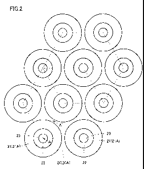
Referring to Figs. 1 and 2, a first embodiment which is one embodiment of the
present invention is described hereinafter. Fig. I is a cross-sectional view
taken along
line A-A' in Fig. 2. Fig. 2 is a plan view of a first main surface 20A in Fig.
I viewed
from above.
Referring to Fig. 1, a MOSFET 1 which is a semiconductor device in the first
embodiment includes an n+ SiC substrate 10 made of SiC which is a wide band
gap
semiconductor as a substrate of an n conductivity type (first conductivity
type), an n
SiC layer 20 as a semiconductor layer of the n conductivity type (first
conductivity type),
a p body 21 as a body region of a p conductivity type (second conductivity
type), an n+
source region 22 as a carrier supply region of the n conductivity type (first
conductivity
type), and a p+ region 23 as a high concentration second conductivity type
region of the
p conductivity type (second conductivity type). N' SiC substrate 10 and n SiC
layer
20 form a SiC wafer 15 which is a semiconductor wafer of the n conductivity
type.
N+ SiC substrate 10 is made of hexagonal SiC, for example, and includes an n
type impurity (impurity of the n conductivity type) of high concentration. N-
SiC layer
20 is formed on one main surface of n+ SiC substrate 10, and has the n
conductivity type
by including an n type impurity. The n type impurity included in n SiC layer
20 is N
-8-
CA 02738680 2011-03-25
110064:910139
(nitrogen), for example, and is included in lower concentration than the n
type impurity
included in n+ SiC substrate 10.
P body 21 is formed in n SiC layer 20 to include first main surface 20A
opposite
to a main surface on which n+ SiC substrate 10 is formed, and has the p
conductivity
type (second conductivity type) by including a p type impurity (impurity of
the p
conductivity type). The p type impurity included in p body 21 is aluminum
(Al), boron
(B), for example, and is included in lower concentration than the n type
impurity
included in n+ SiC substrate 10. Referring to Fig. 2, a plurality of p bodies
21 are
formed, each of which has a circular shape when viewed two-dimensionally. In
addition, each of p bodies 21 is arranged to be positioned at a vertex of a
regular
hexagon when viewed two-dimensionally.
N+ source region 22 is formed within p body 21 to include first main surface
20A
and to be surrounded by p body 21. N+ source region 22 includes an n type
impurity
such as P, As in higher concentration than the n type impurity included in n-
SiC layer
20. In addition, n+ source region 22 is arranged concentrically with p body 21
and has
a circular shape when viewed two-dimensionally, and each of n+ source regions
22 is
arranged to be positioned at a vertex of a regular hexagon in a manner similar
to p body
21.
P+ region 23 is formed within n+ source region 22 to include first main
surface
20A. P+ region 23 includes a p type impurity such as Al, B in higher
concentration
than the p type impurity included in p body 21. In addition, p+ region 23 is
arranged
concentrically with n+ source region 22 and has a circular shape when viewed
two-
dimensionally, and each of p+ regions 23 is arranged to be positioned at a
vertex of a
regular hexagon in a manner similar to p body 21 and n+ source region 22.
Referring to Fig. 1, MOSFET 1 further includes a gate oxide film 30 as an
insulating film, a gate electrode 40, an interlayer insulating film 50, a
source ohmic
electrode 60, a source line 70, and a drain ohmic electrode 80.
Gate oxide film 30 is formed in contact with first main surface 20A to extend
-9-
CA 02738680 2011-03-25
110064: 910139
from a region covering a surface of n+ source region 22 to a region covering a
surface of
p body 21 (region where n+ source region 22 is not formed) and a region
covering a
surface of n SiC layer 20 (region where p body 21 is not formed). Gate oxide
film 30
is made of silicon dioxide (SI02), for example.
Gate electrode 40 is formed in contact with gate oxide film 30 to extend from
the region covering the surface of n+ source region 22 to the region covering
the surface
of p body 21 (region where n+ source region 22 is not formed) and the region
covering
the surface of n SiC layer 20 (region where p body 21 is not formed). Gate
electrode
40 is made of a conductor such as polysilicon, Al.
Source ohmic electrode 60 is formed on first main surface 20A in contact with
n+
source region 22 and p+ region 23. Source ohmic electrode 60 is made of a
material
such as NiSi (nickel silicide), which is capable of establishing ohmic contact
with n+
source region 22 and p+ region 23.
Source line 70 is formed on and in contact with source ohmic electrode 60 on
first main surface 20A. Source line 70 is made of a conductor such as Al.
Drain ohmic electrode 80 is formed in contact with a main surface of n+ SiC
substrate 10 opposite to the main surface on which n SiC layer 20 is formed.
Drain
ohmic electrode 80 is made of a material such as NiSi, which is capable of
establishing
ohmic contact with n+ SiC substrate 10, and is electrically connected to n+
SiC substrate
10.
Interlayer insulating film 50 is disposed on gate oxide film 30 to surround
gate
electrode 40. Interlayer insulating film 50 is made of an insulator such as
SiO2. Thus,
gate electrode 40 and source line 70 are isolated from each other.
That is, MOSFET 1 as a semiconductor device in the first embodiment includes
SiC wafer 15 of the n conductivity type, the plurality of p bodies 21 of the p
conductivity type formed to include first main surface 20A of SiC wafer 15,
and n+
source regions 22 of the n conductivity type formed in regions surrounded by
the
plurality of p bodies 21, respectively, when viewed two-dimensionally. P body
21 has
-10-
CA 02738680 2011-03-25
110064: 910139
a circular shape when viewed two-dimensionally, and n+ source region 22 is
arranged
concentrically with p body 21 and has a circular shape when viewed two-
dimensionally.
Additionally, each of the plurality of p bodies 21 is arranged to be
positioned at a vertex
of a regular hexagon when viewed two-dimensionally.
Operation of MOSFET 1 is described next. Referring to Fig. 1, when gate
electrode 40 has a voltage of not more than a threshold value, i.e., in an off
state, p body
21 located immediately below gate oxide film 30 and n SiC layer 20 are reverse
biased,
to enter anon-conducting state. As a positive voltage is applied to gate
electrode 40,
an inversion layer is formed in a channel region 21A near a portion in contact
with gate
oxide film 30 in p body 21. Asa result, n+ source region 22 and n SiC layer 20
are
electrically connected to each other, causing a current to flow between source
line 70
and drain ohmic electrode 80.
Referring now to Figs. 1 to 14, a method of manufacturing MOSFET I in the
first embodiment is described. Figs. 3, 4, 6, and 8 to 14 are cross-sectional
views
corresponding to the cross section in Fig. 1. Figs. 5 and 7 are plan views of
first main
surface 20A viewed from above, in a manner similar to the case in Fig. 2.
In the method of manufacturing MOSFET 1 of the present embodiment, first, a
step of preparing a substrate is performed. Specifically, referring to Fig. 3,
n+ SiC
substrate 10 which is made of hexagonal SiC, for example, and has the n
conductivity
type by including the n type impurity is prepared.
Next, a step of forming n SiC layer 20 is performed. Specifically, referring
to
Fig. 3, n SiC layer 20 is formed on n+ SiC substrate 10 by epitaxial growth.
The
epitaxial growth can be carried out by employing mixed gas of SiH4 (silane)
and C3H8
(propane) as a source gas, for example. Here, nitrogen is introduced as the n
type
impurity, for example. Consequently, n SiC layer 20 including the n type
impurity in
lower concentration than the n type impurity included in n+ SiC substrate 10
can be
formed.
Next, a step of forming n+ source region 22 is performed. Specifically,
-11-
CA 02738680 2011-03-25
110064:910139
referring to Figs. 3 to 5, first, an oxide film made of SiO2 is formed on
first main surface
20A by CVD (Chemical Vapor Deposition), for example. Then, a resist is applied
to
the oxide film, followed by exposure and development, to form a resist film
having an
opening in a region corresponding to arrangement and a shape of desired n+
source
region 22. Then, the oxide film is partially removed by RIE (Reactive Ion
Etching), for
example, with this resist film as a mask, to form a mask layer formed of the
oxide film
having an opening pattern on n SiC layer 20. The resist film is removed
thereafter,
and then ions are implanted into n SiC layer 20 with this mask layer as a
mask, to form
n+ source region 22 having a circular shape in n SiC layer 20 such that n+
source region
22 is positioned at each vertex of a regular hexagon when viewed two-
dimensionally
(see Fig. 5). For the ion implantation, P may be employed as an n type
impurity, for
example.
Next, a step of forming p body 21 is performed. P body 21 can be formed by a
self-align process as described below. Specifically, first, the mask layer
formed of the
oxide film that was used for forming n+ source region 22 is subjected to
isotropic
etching, to isotropically enlarge the opening of the mask layer. Then, ions
are
implanted into n SiC layer 20 with this mask layer as a mask, to form p body
21
surrounding n+ source region 22 as shown in Figs. 6 and 7. For the ion
implantation,
Al may be employed as a p type impurity, for example.
Next, a step of forming p+ region 23 is performed. In this step, first, the
mask
layer that was used for forming p body 21 is removed. Then, in a manner
similar to the
formation of n+ source region 22, a mask layer formed of an oxide film having
an
opening pattern corresponding to arrangement and a shape of p+ region 23 is
formed,
and ions are implanted into n SiC layer 20 with this mask layer as a mask.
Consequently, p+ region 23 having a circular shape when viewed two-
dimensionally is
formed in a region surrounded by n+ source region 22. For the ion
implantation, Al
may be employed as a p type impurity, for example.
Next, an activation annealing step is performed. Specifically, n SiC layer 20
-12-
CA 02738680 2011-03-25
110064:910139
into which the ions were implanted in the above process is heated, to activate
the
introduced impurity.
Next, a step of forming gate oxide film 30 is performed. In this step,
referring
to Figs. 8 and 9, if SiC layer 20 in which an ion-implanted region was formed
in the
above step is thermally oxidized. Consequently, gate oxide film 30 made of
silicon
dioxide (S102) is formed to cover first main surface 20A.
Next, a step of forming gate electrode 40 is performed. In this step,
referring
to Figs. 9 and 10, first, a resist film having an opening corresponding to a
shape of
desired gate electrode 40 is formed above first main surface 20A. Then, a
polysilicon
film is formed by CVD, for example, above first main surface 20A above which
the
resist film was formed. The polysilicon film on the resist film is then
removed along
with the resist film (lift-off), to form gate electrode 40.
Next, a step of forming interlayer insulating film 50 is performed. In this
step,
first, interlayer insulating film 50 formed of a SiO2 film is formed by CVD,
for example,
to cover first main surface 20A as shown in Fig. 11. Then, a resist film
having an
opening in a desired region is formed, for example, and RIE is performed with
this resist
film as a mask, to form a through hole in interlayer insulating film 50.
Consequently, as
shown in Fig. 12, a contact hole 50A passing through interlayer insulating
film 50 in a
thickness direction to expose p+ region 23 and n+ source region 22 is formed.
With this
process, interlayer insulating film 50 surrounding gate electrode 40 is
completed.
Next, a step of forming source ohmic electrode 60 and drain ohmic electrode 80
is performed. Specifically, first, a Ni film is formed on first main surface
20A, with the
resist film that was used for forming contact hole 50A being left. Then, the
Ni film on
the resist film is removed along with the resist film, to leave the Ni film in
contact with
p+ region 23 and n+ source region 22 exposed through contact hole 50A formed
in
interlayer insulating film 50. This Ni film is then heated and silicidized, to
complete
source ohmic electrode 60 made of NiSi (see Fig. 13). Further, a Ni film is
formed on
the main surface of n+ SiC substrate 10 opposite to the main surface on which
n SiC
- 13 -
CA 02738680 2011-03-25
110064: 910139
layer 20 is formed, and this Ni film is then silicidized, to form drain ohmic
electrode 80
made of NiSi (see Fig. 14). To simplify the manufacturing process, source
ohmic
electrode 60 and drain ohmic electrode 80 can be formed simultaneously.
Next, a step of forming source line 70 is performed. In this step, referring
to
Figs. 14 and 1, an Al film is formed in contact with a surface of source ohmic
electrode
60, for example, to form source line 70. With the process described above,
MOSFET
1 in the first embodiment is completed.
When the mask layer used for forming p body 21 is prepared by performing
isotropic etching on the mask layer that was used for forming n+ source region
22 as
described above, if p body 21 and n+ source region 22 have a conventional
hexagonal
shape, then the opening of the mask used for forming p body 21 has a shape
rounded
near the vertices, which causes increase in difference between a shape of p
body 21
actually formed and a design shape of p body 21 which should be a homothetic
shape to
n+ source region 22. This results in difficulty in stabilizing a reverse
breakdown
voltage of an obtained MOSFET.
In contrast, since a circular shape is employed as a plane shape of a cell in
MOSFET 1 above, the plane shapes of p body 21 and n+ source region 22 are
concentric
circular shapes. Accordingly, even if the self-align process is employed to
form p body
21 as described above, for example, the shape of the opening of the mask in
forming p
body 21 and the shape of the opening of the mask in forming n+ source region
22 can be
readily maintained to be substantially homothetic to each other. Therefore,
the
difference between the shape of p body 21 actually formed and the design shape
of p
body 21 which should be a homothetic shape to n+ source region 22 can be made
small.
MOSFET I above is therefore a MOSFET having a stable reverse breakdown
voltage.
Moreover, in MOSFET I above in which a circular shape is employed as the
plane shape of a cell, a channel length (thickness of p body 21 surrounding n+
source
region 22 in Fig. 2) is substantially the same in all directions. Accordingly,
formation
of an ineffective channel region which occurs such as when a conventional
hexagonal
-14-
CA 02738680 2011-03-25
110064: 910139
cell is employed is suppressed, thereby substantially increasing a channel
width. As a
result, resistance per unit area during forward bias, i.e., on-resistance, is
reduced.
As described above, MOSFET 1 is a semiconductor device achieving a stable
reverse breakdown voltage and reduced on-resistance.
(Second Embodiment)
Referring now to Fig. 15, a second embodiment which is another embodiment of
the present invention is described. Fig. 15 is a plan view of first main
surface 20A in
Fig. 1 viewed from above, and corresponds to. Fig. 2 described in the first
embodiment.
MOSFET I as a semiconductor device in the second embodiment basically has a
similar structure to MOSFET I in the first embodiment above, can be
manufactured in a
similar manner, and has a similar effect. MOSFET 1 in the second embodiment is
different from the first embodiment, however, in terms of the plane shapes of
p body 21,
n+ source region 22 and p+ region 23, i.e., the plane shape of a cell.
Namely, referring to Fig. 15, p body 21 has a regular octagonal shape when
viewed two-dimensionally in MOSFET 1 of the second embodiment. In addition, n+
source region 22 and p+ region 23 are arranged such that their centroids
coincide with
the centroid of p body 21 and have a homothetic shape to p body 21 when viewed
two-
dimensionally.
In MOSFET I of the second embodiment, since a regular octagonal shape is
employed as the plane shape of a cell, the plane shapes of p body 21 and n+
source
region 22 are regular octagonal shapes with coinciding centroids. This leads
to a larger
angle formed by the sides than when a conventional hexagonal cell is employed.
Accordingly, even if the self-align process is employed to form p body 21 as
in the first
embodiment, for example, the shape of the opening of the mask in forming p
body 21
and the shape of the opening of the mask in forming n+ source region 22 can be
readily
maintained to be substantially homothetic to each other. Therefore, the
difference
between the shape of p body 21 actually formed and the design shape of p body
21
which should be a homothetic shape to n+ source region 22 can be made small.
-15-
CA 02738680 2011-03-25
110064:910139
MOSFET 1 in the second embodiment is therefore a MOSFET having a stable
reverse
breakdown voltage.
Moreover, in MOSFET 1 above in which a regular octagonal shape, i.e., a more
circular shape than the conventional shape is employed as the plane shape of a
cell,
variation in channel length depending on a direction becomes smaller.
Accordingly,
formation of an ineffective channel region which occurs such as when a
conventional
hexagonal cell is employed is suppressed, thereby substantially increasing the
channel
width. As a result, resistance per unit area during forward bias, i.e., on-
resistance, is
reduced.
As described above, MOSFET I in the second embodiment is a semiconductor
device achieving a stable reverse breakdown voltage and reduced on-resistance.
(Third Embodiment)
Referring now to Figs. 16 and 17, a third embodiment which is yet another
embodiment of the present invention is described. Fig. 16 is a cross-sectional
view
taken along line B-B' in Fig. 17. Fig. 17 is a cross-sectional view of a JFET
2 viewed
from above, which has been cut on a plane including a first main surface 120A
in Fig. 16.
JFET 2 as a semiconductor device in the third embodiment has a similar
structure to that in the first embodiment in terms of the plane shape and
arrangement of
a cell, and has a similar effect. Impurities introduced to the respective
regions,
electrodes and the like can also include elements similar to those in the
first embodiment.
Specifically, JFET 2 in the third embodiment includes an n+ SiC substrate 110
made of SiC as a substrate of the n conductivity type, an n SiC layer 120 as a
semiconductor layer of the n conductivity type, a p body 121 as a body region
of the p
conductivity type, a channel layer 190 of the n conductivity type, a gate
region 200 of
the p conductivity type, an n+ source region 122 as a carrier supply region of
the n
conductivity type, and a p+ region 123 as a high concentration second
conductivity type
region of the p conductivity type. N+ SiC substrate 110 and n SiC layer 120
form a
SiC wafer 115 which is a semiconductor wafer of the n conductivity type. N+
SiC
-16-
CA 02738680 2011-03-25
110064: 910139
substrate 110, n SiC layer 120, and p body 121 correspond to n' SiC substrate
10, n
SiC layer 20, and p body 21 in the first embodiment, respectively, and have a
similar
structure. Referring to Fig. 17, a plurality of p bodies 121 are formed, each
of which
has a circular shape when viewed two-dimensionally. In addition, each of p
bodies 121
is arranged to be positioned at a vertex of a regular hexagon when viewed two-
dimensionally.
Channel layer 190 is formed on first main surface 120A of if SiC layer 120
opposite to a main surface on which n' SiC substrate 110 is formed, and
extends from a
surface of a region where p body 121 is formed to a surface of a region where
p body
121 is not formed. Gate region 200 is disposed in contact with channel layer
190 to
extend over channel layer 190.
N' source region 122 has an outer peripheral surface having a thickness in
contact with p body 121, channel layer 190, and gate region 200, is arranged
concentrically with p body 121 and has a circular shape when viewed two-
dimensionally,
and each of n' source regions 122 is arranged to be positioned at a vertex of
a regular
hexagon in a manner similar to p body 121.
P' region 123 is formed to be surrounded by n' source region 122, is arranged
concentrically with n' source region 122 and has a circular shape when viewed
two-
dimensionally, and each of p' regions 123 is arranged to be positioned at a
vertex of a
regular hexagon in a manner similar to p body 121 and n' source region 122.
Referring to Fig. 16, JFET 2 further includes a gate electrode 140, an
interlayer
insulating film 150, a source ohmic electrode 160, a source line 170, and a
drain ohmic
electrode 180.
Gate electrode 140 is formed in contact with gate region 200 to extend from a
region facing p body 121 with gate region 200 and channel layer 190 interposed
therebetween to a region not facing p body 121.
Source ohmic electrode 160 is formed in contact with n' source region 122 and
p region 123. Source line 170 is formed on and in contact with source ohmic
-17-
CA 02738680 2011-03-25
110064: 910139
electrode 160. Drain ohmic electrode 180 is formed in contact with a main
surface of
n+ SiC substrate 110 opposite to a main surface on which n SiC layer 120 is
formed.
Interlayer insulating film 150 is disposed between source ohmic electrode 160,
source line 170 and gate electrode 140 to surround gate electrode 140. Thus,
gate
electrode 140 and source line 170, source ohmic electrode 160 are isolated
from each
other.
That is, JFET 2 as a semiconductor device in the third embodiment includes SiC
wafer 115 of the n conductivity type, the plurality of p bodies 121 of the p
conductivity
type formed to include first main surface 120A of SiC wafer 115, and n+ source
regions
122 of the n conductivity type formed in regions surrounded by the plurality
of p bodies
121, respectively, when viewed two-dimensionally. P body 121 has a circular
shape
when viewed two-dimensionally, and n+ source region 122 is arranged
concentrically
with p body 121 and has a circular shape when viewed two-dimensionally.
Additionally, each of the plurality of p bodies 121 is arranged to be
positioned at a
vertex of a regular hexagon when viewed two-dimensionally.
Operation of JFET 2 is described next. There are normally-off type JFETs and
normally-on type JFETs in terms of operation, and one of them can be selected
by
adjusting a thickness and impurity concentration of channel layer 190. Here,
JFET 2 of
normally-on type is described.
Referring to Fig. 16, when gate electrode 140 has a potential the same as that
of
source line 170, a region in channel layer 190 sandwiched between gate
electrode 140
and p body 121 is not completely depleted, so that source line 170 and drain
ohmic
electrode 180 are electrically connected to each other via source ohmic
electrode 160, n+
source region 122, channel layer 190, n SiC layer 120, and n+ SiC substrate
110.
Accordingly, application of a voltage across source line 170 and drain ohmic
electrode
180 causes a current to flow between source line 170 and drain ohmic electrode
180.
As the potential of gate electrode 140 is lowered with respect to that of
source
line 170, depletion of the region in channel layer 190 sandwiched between gate
electrode
-18-
CA 02738680 2011-03-25
110064:910139
140 and p body 121 progresses, causing electrical cutoff between n+ source
region 122
and n SiC layer 120. Accordingly, application of a voltage across source line
170 and
drain ohmic electrode 180 does not cause a current flow.
Referring now to Figs. 16 to 28, a method of manufacturing JFET 2 in the third
embodiment is described. Figs. 18 to 28 are cross-sectional views
corresponding to the
cross section in Fig. 16.
In the method of manufacturing JFET 2 of the present embodiment, first, a step
of preparing n+ SiC substrate 110 and a step of forming n SiC layer 120 are
performed.
These steps can be performed in a manner similar to the first embodiment.
Consequently, SiC wafer 115 having n SiC layer 120 formed on n+ SiC substrate
110 is
completed as shown in Fig. 18.
Next, a step of forming p body 121 is performed. In this step, first, a mask
layer formed of an oxide film having an opening corresponding to a shape of
desired p
body 121 is formed. Then, ions are implanted with this mask layer as a mask,
to form
p body 121 having a circular plane shape as shown in Fig. 19.
Next, a step of forming channel layer 190 is performed. Specifically,
referring
to Fig. 20, channel layer 190 including an n type impurity is formed on first
main surface
120A by epitaxial growth, for example.
Next, a step of forming n+ source region 122 and a step of forming p+ region
123
are performed. Specifically, referring to Figs. 20 and 21, first, channel
layer 190 is
partially removed by etching. Consequently, a central portion of p body 121
having a
circular shape is exposed through channel layer 190. Next, referring to Figs.
21 and 22,
mask layers having openings corresponding to n+ source region 122 and p+
region 123
are formed, respectively, and ions are implanted sequentially in a manner
similar to the
formation of p body 121, to form n+ source region 122 and p+ region 123.
Next, a step of forming gate region 200 is performed. In this step, referring
to
Fig. 23, a mask layer is formed which has an opening corresponding to
remaining
channel layer 190 into which the ions were not implanted in the above steps of
forming
-19-
CA 02738680 2011-03-25
110064:910139
n+ source region 122 and p+ region 123, and ions are implanted with this mask
layer as a
mask. Consequently, gate region 200 into which a p type impurity was
introduced is
formed.
Next, an activation annealing step is performed. In this step, the region into
which the ions were implanted in the above process is heated, to activate the
introduced
impurity.
Next, a step of forming gate electrode 40 is performed. In this step,
referring
to Figs. 23 and 24, a resist film having an opening corresponding to a shape
of desired
gate electrode 140 is formed, and then a polysilicon film is formed by CVD,
for example.
The polysilicon film on the resist film is then removed along with the resist
film, to form
gate electrode 140.
Next, a step of forming interlayer insulating film 150 is performed. In this
step,
first, interlayer insulating film 150 formed of a Si02 film, for example, is
formed to
entirely cover a region over first main surface 120A as shown in Fig. 25.
Then, after a
resist film having an opening in a desired region is formed, RIE is performed
with this
resist film as a mask, to form a through hole in interlayer insulating film
150.
Consequently, as shown in Fig. 26, a contact hole 150A passing through
interlayer
insulating film 150 in a thickness direction to expose p+ region 123 and n+
source region
122 is formed. With this process, interlayer insulating film 150 surrounding
gate
electrode 140 is completed.
Next, a step of forming source ohmic electrode 160 and drain ohmic electrode
180 is performed. Specifically, first, a Ni film is formed on first main
surface 120A,
with the resist film that was used for forming contact hole 150A being left.
Then, the
Ni film on the resist film is removed along with the resist film, to leave the
Ni film in
contact with p+ region 123 and n+ source region 122 exposed through contact
hole
150A formed in interlayer insulating film 150. This Ni film is then heated and
silicidized, to complete source ohmic electrode 160 made of NiSi as shown in
Fig. 27.
Further, a Ni film is formed on the main surface of n+ SiC substrate 110
opposite to the
-20-
CA 02738680 2011-03-25
110064:910139
main surface on which n SiC layer 120 is formed, and this Ni film is
silicidized, to form
drain ohmic electrode 180 made of NiSi as shown in Fig. 28. To simplify the
manufacturing process, source ohmic electrode 160 and drain ohmic electrode
180 can
be formed simultaneously.
Next, a step of forming source line 170 is performed. In this step, referring
to
Figs. 28 and 16, an Al film is formed in contact with a surface of source
ohmic electrode
160, for example, to form source line 170. With the process described above,
JFET 2
in the third embodiment is completed.
In JFET 2 of the present embodiment, a circular shape is employed as the plane
shape of a cell in a manner similar to MOSFET 1 in the first embodiment.
Accordingly,
JFET 2 is a semiconductor device achieving a stable reverse breakdown voltage
and
reduced on-resistance.
While a circular shape is employed as the plane shape of a cell in the third
embodiment above, the circular shape may be replaced with a regular polygonal
shape
with seven or more vertices such as a regular octagonal shape as in the second
embodiment, or a polygonal shape with even more vertices such as a regular
polygonal
shape with twenty or more vertices.
Further, while a MOSFET and a JFET are described as examples of the
semiconductor device according to the present invention in the embodiments
above, the
semiconductor device according to the present invention is not limited as
such, but may
be an IGBT, for example. Furthermore, while a substrate and a semiconductor
layer
are made of SiC in the semiconductor device according to the present invention
in the
embodiments above, the semiconductor device according to the present invention
is not
limited as such. As a material for the substrate and the semiconductor layer
of the
semiconductor device according to the present invention, Si may be employed,
or a wide
band gap semiconductor such as GaN (gallium nitride) may be employed.
It should be understood that the embodiments disclosed herein are illustrative
and non-restrictive in every respect. The scope of the present invention is
defined by
-21-
CA 02738680 2011-03-25
110064: 910139
the terms of the claims, rather than the description above, and is intended to
include any
modifications within the scope and meaning equivalent to the terms of the
claims.
INDUSTRIAL APPLICABILITY
The semiconductor device according to the present invention is advantageously
applicable particularly to a semiconductor device required to have a stable
reverse
breakdown voltage and reduced on-resistance.
DESCRIPTION OF THE REFERENCE SIGNS
1 MOSFET; 2 JFET; 10, 110 n SiC substrate; 15, 115 SiC wafer; 20, 120 n
SiC layer; 20A, 120A first main surface; 21, 121 p body; 21A channel region;
22, 122 n+
source region; 23 123 p+ region; 30 gate oxide film; 40, 140 gate electrode;
50, 150
interlayer insulating film; 50A, 150A contact hole; 60, 160 source ohmic
electrode; 70,
170 source line; 80, 180 drain ohmic electrode; 190 channel layer; 200 gate
region.
-22-