Note: Descriptions are shown in the official language in which they were submitted.
CA 02738844 2011-05-04
PATENT
Attorney Docket No.: OCO-188-CA
PATENT APPLICATION FOR CANADA
TITLE: Full Wave AC/DC Voltage Divider
FIELD OF THE INVENTION
[0001] The present subject matter relates to voltage dividers. More
particularly, the
present subject matter relates to a full wave, series charge, parallel
discharge capacitive
voltage divider configured to provide a DC voltage from an AC supply.
BACKGROUND OF THE INVENTION
[0002] Power supplies constructed using the known concept of serially charging
a
series of capacitors and discharging the series in parallel are known in the
art. Such
configurations may be used, for example, with variations in excitation, for a
variety of
configurations. In one example, U.S. Pat. No. 5,446,644 (Zhou) discloses a
direct current
(DC) voltage divider configuration employing a diode and capacitor
configuration. In
such '644 patent configuration, a DC supply is applied as the input to a diode
and
capacitor series circuit by way of a first switch. A second switch is
configured to couple a
number of diodes to the series connected capacitors to provide a parallel
discharge path.
Generally, such arrangement operates as a voltage divider in order to convert
a relatively
higher DC voltage to a relatively lower DC voltage. With an input DC voltage
to such
circuit, Zhou operates the switches alternately at a frequency chosen to
produce a desired
output voltage level. Such form of operation results in a somewhat selectively
variable
output voltage but at the cost of complex variable frequency alternating
operation of such
two switches.
[0003] Cubbison, Jr. (U.S. Pat. No. 4,649,468) discloses a voltage divider
circuit
employing a series charge/parallel discharge diode/capacitor circuit where the
diodes
CA 02738844 2011-05-04
2
provide the switching without additional switches. The circuit in such
Cubbison, Jr.
arrangement, however, provides sub-divided capacitors, with varying numbers of
capacitors used directly connected in series to provide desired low voltage
outputs.
[0004] An "Analog Devices" article illustrates the use of a capacitor divider
power
supply in an electric meter. See, Analog Devices Application Note AN-687, "A
Low Cost
Tamper-Resistant Energy Meter Based on the ADE7761 with Missing Neutral
Function"
by English and Moulin, 2004, including material starting on page 7 of such
publication
under the title "Power Supply Design." A Linear Technology Magazine article
illustrates
a switch capacitor voltage regulator that is configured to provide current
gain. See,
Design Ideas, "Switched Capacitor Voltage Regulator Provides Current Gain"
Linear
Technology Magazine, February 1999.
[0005] Despite some benefits offered by such configurations and others, it
would,
nevertheless, be beneficial to provide a simplified series-parallel capacitor-
rectifier
voltage dividing circuit that was able to produce a regulated DC voltage from
an
alternating current (AC) input source.
[0006] While various implementations of series-parallel capacitor-rectifier
voltage
dividing circuits have been developed, and while various combinations of
voltage divider
circuits have been developed, no design has emerged that generally encompasses
all of
the desired characteristics as hereafter presented in accordance with the
subject
technology.
SUMMARY OF THE INVENTION
[0007] - In view of the recognized features encountered in the prior art and
addressed
by the present subject matter, improved apparatus and methodology are provided
for
converting an AC source voltages to a DC voltage.
[0008] In an exemplary configuration, a full wave capacitive voltage divider
power
supply for reducing an alternating current (AC) from an AC source to a direct
current
(DC) is provided comprising at least one pair of full wave rectifiers each
comprising a
plurality of rectifiers and a capacitor. The pair of full wave rectifiers may
be coupled in
series such that the capacitors are charged in series during portions of both
a positive and
negative half cycle of an applied AC source. A pair of switches may be
associated with
CA 02738844 2011-05-04
3
each of the pair of full wave rectifiers and configured to be non-conductive
during the
charging portions of both a positive and negative half cycle of an applied AC
source and
conductive during a time period spanning a period on either side of and
including the zero
crossing point of the applied AC source. A load capacitor is provided and the
switches
are configured to provide parallel discharge paths from each of the capacitors
to the load
capacitor.
[0009] In selected embodiments, a resistor is coupled in series with the
applied AC
source and the pair of full wave rectifiers. In certain embodiments a second
load capacitor
is couple in series with the load capacitor and a common terminal between the
second
load capacitor and the load capacitor is coupled to a common line of the
applied AC
source so that both positive and negative direct current voltage relative to
the common
line of the applied AC source may be provided.
[0010] In particular embodiments at least one additional full wave rectifier
and
capacitor is coupled in series with the at least one pair of full wave
rectifiers and at least
one additional pair of switches is associated with said at least on additional
full wave
rectifier. The additional pair of switches is configured to be non-conductive
during the
charging portions of both a positive and negative half cycle of an applied AC
source and
conductive during a time period spanning a period on either side of and
including the zero
crossing point of the applied AC source.
[0011] In other embodiments of the present subject matter, a full wave
capacitive
voltage divider is provided comprising a plurality of full wave rectifiers
each
corresponding to a plurality of rectifiers and a capacitor. The plurality of
full wave
rectifiers are coupled in series such that the capacitors of each of the
plurality of full wave
rectifiers are charge in series during portions of both a positive and
negative half cycle of
an applied AC source. A pair of switches is associated with each of the
plurality of full
wave rectifiers and configured to be non-conductive during the charging
portions of both
a positive and negative half cycle of an applied AC source and conductive
during a time
period spanning a period on either side of and including the zero crossing
point of the
applied AC source. A load capacitor is coupled to the pair of switches so that
when the
pair of switches is conductive, each of the capacitors of each of the
plurality of full wave
rectifiers is discharged in parallel into the load capacitor.
CA 02738844 2011-05-04
4
[0012] The present subject matter also relates to power supply methodology for
converting an alternating current (AC) from an AC source to a direct current
(DC). An
exemplary method comprises providing at least one pair of full wave rectifiers
each
configured as a plurality of rectifiers and a capacitor. The full wave
rectifier pairs are
coupled in series and an AC source is applied to the pair such that the
capacitors are
charged in series during portions of both a positive and negative half cycle
of the applied
AC source. A pair of switches is associated with each of the pair of full wave
rectifiers
and configured to be non-conductive during the charging portions of both a
positive and
negative half cycle of an applied AC source and conductive during a time
period spanning
a period on either side of and including the zero crossing point of the
applied AC source.
A load capacitor is provided and the switches are configured to provide
parallel discharge
paths from each of the capacitors to the load capacitor.
[0013] In certain embodiments, the methodology provides for coupling a
resistor in
series with the applied AC source and the pair of full wave rectifiers. In
particular
embodiments, the methodology provides for coupling a second load capacitor in
series
with the load capacitor, and coupling a common terminal between the second
load
capacitor and the load capacitor to a common line of the applied AC source.
[0014] One present exemplary embodiment in accordance with the present subject
matter relates to a full wave capacitive voltage divider power supply for
converting an
alternating current (AC) from an AC source to a direct current (DC). Such
present
exemplary power supply preferably may comprise at least one pair of full wave
rectifiers,
each comprising a plurality of rectifiers and a rectifier capacitor, such pair
of full wave
rectifiers coupled in series such that such rectifier capacitors are charged
in series during
portions of both a positive and negative half cycle of an applied AC source; a
pair of
switches associated with each of such pair of full wave rectifiers, such
switches
configured to be non-conductive during the charging portions of both a
positive and
negative half cycle of an applied AC source, and configured to be conductive
during a
time period spanning a period on either side of and including the zero
crossing point of
the applied AC source; and a load capacitor, wherein such switches are
configured to
provide parallel discharge paths from each of such rectifier capacitors to
such load
capacitor.
CA 02738844 2011-05-04
[0015] In some present alternative, such an exemplary power supply may further
comprise a resistor coupled in series with the applied AC source and such pair
of full
wave rectifiers. In other present alternatives, a present exemplary power
supply may
further comprise a second load capacitor couple in series with such load
capacitor,
wherein a common terminal between such second load capacitor and such load
capacitor
may be coupled to a common line of the applied AC source, whereby both
positive and
negative direct current voltage relative to the common line of the applied AC
source may
be provided.
[0016] Still other present alternative power supplies may further comprise at
least one
additional full wave rectifier and rectifier capacitor coupled in series with
such at least
one pair of full wave rectifiers; and at least one additional pair of switches
associated with
such at least one additional full wave rectifier, such at least one additional
pair of
switches configured to be non-conductive during the charging portions of both
a positive
and negative half cycle of an applied AC source and conductive during a time
period
spanning a period on either side of and including the zero crossing point of
the applied
AC source.
[0017] Another present exemplary embodiment of the present technology may
relate
to a full wave capacitive voltage divider, comprising a plurality of full wave
rectifiers
each comprising a plurality of rectifiers, and a rectifier capacitor, the
plurality of full
wave rectifiers coupled in series such that such capacitors of each of the
plurality of full
wave rectifiers are charged in series during portions of both a positive and
negative half
cycle of an applied AC source; a pair of switches associated with each of such
plurality of
full wave rectifiers, such pair of switches configured to be non-conductive
during the
charging portions of both a positive and negative half cycle of an applied AC
source and
conductive during a time period spanning a period on either side of and
including the.zero
crossing point of the applied AC source; and a load capacitor coupled to such
pair of
switches. Per such present exemplary arrangement, advantageously, when such
pair of
switches is conductive, each of such rectifier capacitors of each of the
plurality of full
wave rectifiers may be discharged in parallel into such load capacitor.
[0018] Variations of such present voltage divider embodiments may further
comprise
a resistor coupled in series with the applied AC source and such pair of full
wave
CA 02738844 2011-05-04
6
rectifiers. Still further, optionally, such load capacitor may comprise a pair
of capacitors
connected in series.
[0019] Those of ordinary skill in the art should understand from the complete
disclosure herewith that the present subject matter equally relates to both
apparatus as
well as to corresponding and related methodology. One present exemplary method
relates to power supply methodology for converting an alternating current (AC)
from an
AC source to a direct current (DC). Such an exemplary method may preferably
comprise
providing at least one pair of full wave rectifiers each configured as a
plurality of
rectifiers and a capacitor; coupling the pair of full wave rectifiers in
series; applying an
AC source to the pair of full wave rectifiers such that the capacitors are
charged in series
during portions of both a positive and negative half cycle of the applied AC
source;
associating a pair of switches with each of the pair of full wave rectifiers;
configuring the
pair of switches to be non-conductive during the charging portions of both a
positive and
negative half cycle of an applied AC source and conductive during a time
period spanning
a period on either side of and including the zero crossing point of the
applied AC source;
providing a load capacitor; and configuring the switches to provide parallel
discharge
paths from each of the respective capacitors of the rectifiers to the load
capacitor.
[0020] Other present variations of such exemplary power supply methodology may
further comprise coupling a resistor in series with the applied AC source and
the pair of
full wave rectifiers. Other variations may further comprise coupling a second
load
capacitor in series with the load capacitor; and coupling a common terminal
between the
second load capacitor and the load capacitor to a common line of the applied
AC source.
[0021] Still further, other optionally present exemplary methodology may
further
include coupling at least one additional full wave rectifier and capacitor in
series with the
at least one pair of full wave rectifiers; associating, at least one
additional pair of switches
with the at least one additional full wave rectifier; and configuring the at
least one
additional pair of switches to be non-conductive during the charging portions
of both a
positive and negative half cycle of an applied AC source and conductive during
a time
period spanning a period on either side of and including the zero crossing
point of the
applied AC source.
[0022] Additional objects and advantages of the present subject matter are set
forth
in, or will be apparent to, those of ordinary skill in the art from the
detailed description
CA 02738844 2011-05-04
7
herein. Also, it should be further appreciated that modifications and
variations to the
specifically illustrated, referred and discussed features and elements hereof
may be
practiced in various embodiments and uses of the present subject matter
without departing
from the spirit and scope of the subject matter. Variations may include, but
are not
limited to, substitution of equivalent means, features, or steps for those
illustrated,
referenced, or discussed, and the functional, operational, or positional
reversal of various
parts, features, steps, or the like.
[0023] Still further, it is to be understood that different embodiments, as
well as
different presently preferred embodiments, of the present subject matter may
include'
various combinations or configurations of presently disclosed features, steps,
or elements,
or their equivalents (including combinations of features, parts, or steps or
configurations
thereof not expressly shown in the figures or stated in the detailed
description of such
figures). Additional embodiments of the present subject matter, not
necessarily expressed
in the summarized section, may include and incorporate various combinations of
aspects
of features, components, or steps referenced in the summarized objects above,
and/or,
other features, components, or steps as otherwise discussed in this
application. Those of
ordinary skill in the art will better appreciate the features and aspects of
such
embodiments, and others, upon review of the remainder of the specification.
BRIEF DESCRIPTION OF THE DRAWINGS
[0024] A full and enabling disclosure of the present subject matter, including
the best
mode thereof, directed to one of ordinary skill in the art, is set forth in
the specification,
which makes reference to the appended figures, in which:
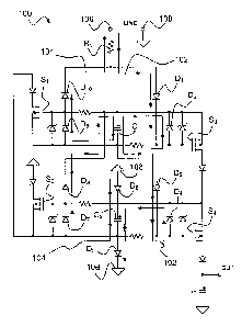
[0025] Figure 1 is a schematic representation of a pair of full wave rectifier
circuits
coupled together in accordance with present technology to provide a voltage
divider
circuit and illustrating the charging paths for associated capacitors;
[00261 Figure 2 duplicates Figure 1 but illustrates the discharging paths for
the
associated capacitors;
[0027] Figure 3 is a schematic representation of a second embodiment of the
present
subject matter illustrating a pair of full wave rectifier circuits coupled
together to provide
CA 02738844 2011-05-04
8
a voltage divider circuit having both positive and negative outputs and
illustrating the
discharging paths for the associated capacitors; and
[0028] Figure 4 is a schematic representation of a plurality of full wave
rectifier
circuits coupled together to provide higher levels of voltage rectification
and division.
[0029] Repeat use of reference characters throughout the present specification
and
appended drawings is intended to represent same or analogous features,
elements, or steps
of the present subject matter.
DETAILED DESCRIPTION OF THE PREFERRED EMBODIMENTS
[0030] As discussed in the Summary of the Invention section, the present
subject
matter is particularly concerned with a full wave, series charge, parallel
discharge
capacitive voltage divider configured to provide a DC voltage from an AC
supply.
[0031] Selected combinations of aspects of the disclosed technology correspond
to a
plurality of different embodiments of the present subject matter. It should be
noted that
each of the exemplary embodiments presented and discussed herein should not
insinuate
limitations of the present subject matter. Features or steps illustrated or
described as part
of one embodiment may be used in combination with aspects of another
embodiment to
yield yet further embodiments. Additionally, certain features may be
interchanged with
similar devices or features not expressly mentioned which perform the same or
similar
function.
[0032] Reference will now be made in detail to the presently preferred
embodiments
of the subject full wave voltage divider. Referring now to the drawings,
Figure 1
illustrates a schematic representation of a pair of full wave rectifier
circuits coupled
together in accordance with present technology to provide a voltage divider
circuit 100
and illustrates charging paths 102, 104 for associated capacitors C1, C2
within the pair of
full wave rectifiers.
[0033] As will be appreciated by those of ordinary skill in the art from an
inspection
of the schematic illustrated in Figure 1, a first full wave rectifier is
formed by a plurality
of rectifier elements, herein illustrated as diodes D1, D2, D9, and D10 that
are configured to
provide charge to capacitor C1 from an alternating current (AC) line source
coupled
across line input terminals 106, 108. Similarly, a second full wave rectifier
is formed by
CA 02738844 2011-05-04
9
a plurality of rectifiers herein illustrated as diodes D3, D4, D79, and D8
that are configured
to provide charge to capacitor C2 from the AC line source coupled across line
input
terminals 106, 108. For reference purposes, line terminal 108 is
representatively
designated as a common potential terminal for all schematic diagrams herein
illustrated.
[0034] Those of ordinary skill in the art should appreciate that rectification
of an AC
source may be provided in a number of ways, generally by using what may be
commonly
referred to as a "rectifier." For present purposes, such rectifiers may be
provided in a
number of ways using diodes as described in the remainder of the
specification, but may
also be provided using electro-mechanical and electro-magnetically operated
switches,
MOSFET devices, SCRs, TRIACs, and other types of solid state switching devices
as
well as such items as vacuum tube devices.
[0035] As may be seen from further inspection of Figure 1, when line terminal
106
goes positive with respect to common terminal 108, charging current will flow
through
resistor R1, and then along a path 102 including diodes D1, D2, capacitor C1,
diodes D3,
D4, capacitor C2, diode D5 and back to common terminal 108. Through such
charging
path, capacitors C1, C2 are charged in series during the positive half cycles
of the voltage
applied to line terminals 106, 108.
[0036] Resistor R1, in addition to providing current control of the charging
path,
provides efficient surge protection for the voltage divider circuit since,
with capacitors C1,
C2 being charged, the overall circuit represents a low-pass filter. In such
manner,
capacitors C1, C2 provide transient protection for the semiconductor devices
during line
surges. Due to the transient protection inherently provided by the present
subject matter,
other commonly used transient suppression devices such as metal oxide
varistors (MOV),
gas discharge tubes (GDT), and other transient voltage suppressor (TVS)
devices are-not
as necessary but may be optionally provided.
[0037] In similar fashion, on the negative half cycles of the line voltage, a
charging
current will flow from common terminal 108 along a path 104 including diode
D6,
capacitor C2, diodes D7, D8, capacitor C1, diodes D9, D10 and back to line
terminal 106.
Again capacitors C1, C2 are charged in series from the AC line voltage applied
across
terminals 106, 108.
[0038] A further inspection of Figure 1 reveals the presence of four switching
devices
identified as switches S1, S2, S3, and S4. In the exemplary configuration
illustrated in
CA 02738844 2011-05-04
Figure 1, such switching devices may correspond to transistors, and, in
particular, to
paired complimentary MOSFET transistors. It should be appreciated, however,
that other
types of switching device may be used. During the majority of both the
positive and
negative half cycles of the AC line voltage applied to terminals 106, 108,
each of such
switches S1, S2, S3, S4 are in a non-conductive state.
[0039] During a portion of the time, in particular, a time period spanning a
period on
either side of and including the zero crossing point of the AC voltage applied
across line
terminals 106, 108, switches Si, S2, S3, and S4 become conductive and provide
discharge
paths for the charge stored in capacitors C1, C2. As switches S1, S2, S3, and
S4 become
conductive, capacitors C1, C2 are then discharged in parallel to provide an
output voltage
for the full wave voltage divider.
[0040] With reference now to Figure 2, it will be seen that Figure 2
duplicates Figure
I but illustrates discharge paths 202, 204 for the associated capacitors C],
C2. In such
instance, when the line voltage applied across terminals 106, 108 approaches
the zero
crossing point, switches S1, S2, S3, and S4 all become conductive and provide
first and
second discharge paths 202, 204 that effectively discharge capacitors C1, C2
in parallel
into output (i.e., load) capacitor C3 that has one terminal thereof coupled to
an output
terminal OUT and a second terminal thereof coupled to common potential at
terminal
108.
[0041] With further reference to Figure 2, it will be seen that first
discharge path 202
is formed from capacitor C1's relatively positive side through now conductive
switches
S3, S4, diode D13, through capacitor C3 and back to the relatively negative
terminal of
capacitor C1 by way of path 206 through common potential terminal 108, diode
D12 and
switch S1. In similar fashion, second discharge path 204 is formed from
capacitor C2
through conductive switch S4, diode D13 and capacitor C3 and back to the
relative negative
terminal of capacitor C2 by way of path 208 through common potential terminal
108,
diode D11 and switch S2.
[0042] In such manner, capacitors C1, C2 are charged in series as previously
described
with respect to Figure 1 and discharged in parallel into capacitor C3. Such
process results
in a divide by two operation so that the AC voltage applied to terminals 106,
108 is
converted to direct current (DC) and applied to capacitor C3 at about half the
original
level of the applied line voltage. One advantage of the divide by two
operation is that the
CA 02738844 2011-05-04
11
various component's voltage ratings require only one half that of the voltage
applied to
line terminals 106, 108. As will be seen in further embodiments, such ratio
may be
further reduced to the point that the component voltage ratings may be
significantly lower
than the voltage applied to line terminals 106, 108.
[0043] With reference to Figure 3, there is illustrated a schematic
representation of a
second embodiment 300 of the present subject matter illustrating a pair of
full wave
rectifier circuits coupled together to provide a voltage divider circuit
having both positive
POS and negative NEG outputs and illustrating the discharging paths 202, 204,
306, 308
for the associated capacitors C1, C2-
[00441 By reference to both Figures 2 and 3, it will be noted that one
additional
component, capacitor C4, has been added to the circuit illustrated in Figure
2. By so
doing, the common point connection 108 connecting diode D11 has been modified
by
placing capacitor C4 in the series circuit through diode D11 and switch S2. An
important
advantage is gained by this relatively simple addition in that a more
symmetrical bipolar
output can be provided while the division ratio increases two times so that
the circuit
operates as a divide by four circuit. A further advantage as alluded to above
comes from
the fact that now the individual component's voltage ratings need only be one
fourth that
of the voltage applied to line terminals 106, 108.
[0045] As the only change made in to the circuit illustrated in Figure 2 is
within the
discharge paths for capacitors C1, C2, it should be appreciated that the
charging paths 202,
204 for capacitors C1, C2 in the embodiment illustrated in Figure 3 are
identical to that
illustrated in Figure 2 and so are designated by identical identifications.
The discharge
paths 306, 308 in this embodiment, however, have shifted somewhat as follows.
[0046] The discharge paths 202, 306 for capacitor C1 as noted are identical to
path
202 of Figure 2, but changed in the Figure 3 embodiment so that after the
discharge
current flows from path 202 through capacitor C3, the discharge path continues
as
discharge path 306 though common terminal 108, capacitor C4, through diode
D11, switch
S2, diode D12, and back to capacitor C1 through switch S1. On the other hand,
discharge
path 204 from capacitor C2 continues through capacitor C3 and back to
capacitor C2, as
discharge path 308 by way of common terminal 108, capacitor C4, diode D11, and
switch
S2.
CA 02738844 2011-05-04
12
[0047] In the instance of both discharge paths 306 and 308, charging voltage
that was
applied to capacitors C1, C2 in series has been discharged into capacitors C3,
C4 in a series
configuration by parallel discharge from capacitors C1, C2. Such operation
produces the
previously mentioned divide by four effect.
[0048] With reference to Figure 4, there is illustrated a schematic
representation of a
plurality of full wave rectifier circuits 400 coupled together to provide
higher levels of
voltage rectification and division. As illustrated in Figure 4, four cells are
configured
such that capacitors C5, C6, C7, and C8 are charged in series and then
discharged in
parallel into capacitor C9. Such functionality produces a full wave divide by
four effect.
In such instance, a low-voltage power supply is created where 240 VAC may be
supplied
to the line input and 60 VDC may be provided from the output terminal OUT.
[0049] Carrying such process forward, substantially any number of cells may be
strung together in a manner identical to that of Figure 3. In one example,
stringing twenty
four cells together would provide a power supply where application of a 14.4
kVAC input
to the line input terminals would provide 600 VDC at the output terminal OUT.
[0050] The present subject matter provides additional benefits from the fact
that the
switching frequency of the various switches is very low, generally only double
the power
line frequency of, for example, 50Hz or 60Hz. Further, the cost of
implementing the full
wave capacitive voltage divider in accordance with present technology is very
low as the
semiconductor and capacitor components are less expensive at the lower voltage
ratings
required.
[0051] It is also possible to fully integrate the present subject matter with
the
exception of the capacitors and, as noted with respect to Figure 4, the
technology is very
scalable so as to be able to provide a wide range of voltage supplies from an
equally wide
range of input voltages. Other features may also be easily implemented. For
example,
low-side voltage regulation may be achieved by controlled interruption of the
discharge
current from the string of cells into a load coupled across the output.
[0052] While the present subject matter has been described in detail with
respect to
specific embodiments thereof, it will be appreciated that those skilled in the
art, upon
attaining an understanding of the foregoing, may readily produce alterations
to, variations
of, and equivalents to such embodiments. Accordingly, the scope of the present
disclosure is by way of example rather than by way of limitation, and the
subject
CA 02738844 2011-05-04
13
disclosure does not preclude inclusion of such modifications, variations
and/or additions
to the present subject matter as would be readily apparent to one of ordinary
skill in the
art.