Note: Descriptions are shown in the official language in which they were submitted.
CA 02740489 2011-05-17
TITLE: METHOD AND APPARATUS FOR OPTIMIZING TRANSMITTER POWER
EFFICIENCY
Field
[0001] Embodiments disclosed herein relate to transmitter power efficiency in
communication systems and in particular to optimizing transmitter power
efficiency in
communication systems.
Background
[0002] Mobile devices, such as radios and cellular telephones, typically rely
on
power from one or more internal batteries. A major performance criterion for
such
devices is the battery life, which is typically defined as the time period for
which the
battery will power the device on a single charge. A large portion of the
battery power is
consumed in a power amplifier (PA) section of the mobile electronic device's
transmitter. The power amplifier section amplifies the power of a signal to be
transmitted
from a comparatively low internal power level to a substantially higher power
level
required for wireless communication with remote base stations or other
devices.
[0003] Power efficiency is even more important with multimedia services that
consume significantly more power than traditional voice communication
services. Thus,
improving the power amplifier efficiency or, more generally, transmitter
efficiency, is an
important factor in battery life performance.
Brief Description of the Figures
[0004] For a better understanding of embodiments of the systems and methods
described herein, and to show more clearly how they may be carried into
effect,
reference will be made, by way of example, to the accompanying drawings, in
which:
[0005] FIG. 1 shows a simplified block diagram of one embodiment of a
transmitter apparatus;
-1-
CA 02740489 2011-05-17
[0006] FIG. 1A shows a simplified block diagram of an alternative embodiment
of
a transmitter apparatus;
[0007] FIG. 2 shows a simplified block diagram of another alternative
embodiment of the transmitter apparatus;
[0008] FIG. 3 shows a simplified block diagram of another alternative
embodiment of the transmitter apparatus;
[0009] FIG. 3A shows a simplified block diagram of another alternative
embodiment of the transmitter apparatus;
[0010] FIG. 4 shows a simplified block diagram of another alternative
embodiment of the transmitter apparatus;
[0011] FIG. 5 shows a simplified block diagram of another alternative
embodiment of the transmitter apparatus;
[0012] FIG. 6 shows a flowchart for a method of optimizing power efficiency in
a
transmitter apparatus, in accordance with at least one embodiment;
[0013] FIG. 7 shows a flowchart for a method of optimizing power efficiency in
a
transmitter apparatus, in accordance with at least one other embodiment; and
[0014] FIG. 8 shows a flowchart for a method of optimizing power efficiency in
a
transmitter apparatus, in accordance with at least one other embodiment.
Detailed Description
[0015] One difficulty in extending battery life is related to the modulation
schemes
now being used in mobile devices. Modulation methods such as code division
multiple
access (CDMA), orthogonal frequency division multiplexing (OFDM), and other
types of
multi-carrier modulations exhibit high peak-to-average power ratios (PAPR).
Further
complicating the problem is the stochastic nature of the required transmitter
power.
These transmitters are required to provide both large dynamic range and good
linearity.
In addition, some standards require quick variation in both output power and
PAPR. For
-2-
CA 02740489 2011-05-17
example, air interface standard CDMA2000 requires provisioning for variations
of up to
800 dB per second.
[0016] Current transmitters are designed for peak power utilization. Thus, at
low
power utilization, the power efficiency is lower than at peak power
utilization. In addition,
some transmitters also incorporate a step control of the quiescent current.
However, in
some cases, this can yield lower power savings. In some cases step control can
be
blended with continuous control. Embodiments described herein relate generally
to
optimizing power efficiency in a transmitter for a mobile device.
[0017] In accordance with one broad aspect, there is provided a transmitter
for a
mobile device comprising: an encoder and modulator for generating an encoded
and
modulated transmit signal based on an input signal; a digital to analog
converter
coupled to the encoder and modulator, for generating an analog representation
of the
encoded and modulated transmit signal; an amplifier stage coupled to the
digital to
analog converter, for amplifying the analog representation of the encoded and
modulated transmit signal to generate a transmission signal; and an amplifier
control
block configured to generate an amplifier control signal for adjusting at
least one
parameter of the amplifier stage, the amplifier control block comprising at
least one
mapper to determine the amplifier control signal based on a peak to average
power
ratio and an average transmit power of the transmission signal.
[0018] In another broad aspect, the amplifier control block can comprise a
first
mapper for generating a first signal representative of the peak to average
power ratio
based on a type of the encoded and modulated transmit signal, a second mapper
for
generating a second signal representative of the average transmit power of the
transmission signal, and a summer for generating the amplifier control signal
based on
the first and second signals.
[0019] In another broad aspect, the amplifier control block can comprise a
mapper configured to generate, for each of a plurality of different peak to
average power
ratios, a corresponding amplifier control signal based on the average transmit
power of
the transmission signal.
-3-
CA 02740489 2011-05-17
[0020] In another broad aspect, the mapper can be configured to generate the
corresponding amplifier control signal further based on one or more
environmental
conditions in which the transmitter is operating. The mapper can be configured
to
generate the corresponding amplifier control signal further based on one or
more
operating conditions of the transmitter, which can comprise transmit frequency
and drive
band.
[0021] In another broad aspect, the amplifier stage can comprise an automatic
gain control amplifier coupled to an output of the digital to analog
converter, and a
power amplifier coupled to an output of the automatic gain control amplifier,
wherein the
amplifier control signal adjusts at least one parameter of the power
amplifier.
[0022] In another broad aspect, the transmitter can further comprise a gain
control block configured to generate an automatic gain control signal for
controlling gain
in the automatic gain control amplifier based on an average transmit power
indicator
corresponding to the average transmit power of the transmission signal.
[0023] In another broad aspect, the transmitter can further comprise a gain
control compensation block coupled with the gain control block in a feedback
loop, and
the gain control compensation block can be configured to generate a gain
correction
factor for the gain control block based on the amplifier control signal. The
gain
correction factor can be applied to the average transmit power indicator
provided to the
gain controller to adjust the automatic gain control signal. The gain
correction factor can
be applied to the automatic gain control signal directly. The gain correction
factor can be
an input to the gain control block, in which case the gain control block can
be configured
to generate the automatic gain control signal based further on the gain
correction factor.
[0024] In another broad aspect, the at least one parameter of the power
amplifier
can comprise at least one of a bias, a current bias, a supply voltage, a stage
switch-in, a
stage switch-out, a turning on, a turning off, a gain, a gain distribution, a
conducting
angle, an amplifier class change, a load, or an impedance.
[0025] In another broad aspect, the amplifier control block can comprise a
plurality of mappers for determining a corresponding plurality of amplifier
control signals
based on the peak to average power ratio and the average transmit power of the
-4-
CA 02740489 2011-05-17
transmission signal. At least one of the plurality of amplifier control signal
can adjust a
supply voltage or current bias of the amplifier stage.
[0026] In another broad aspect, the amplifier control signal and the analog
representation of the encoded and modulated transmit signal can be delay
aligned.
[0027] In another broad aspect, the amplifier control signal can be advanced
in
time with respect to the analog representation of the encoded and modulated
transmit
signal.
[0028] In another broad aspect, the analog representation of the encoded and
modulated transmit signal can be delayed in time with respect to the amplifier
control
signal.
[0029] In another broad aspect, at least one of the encoder and modulator,
digital
to analog converter, and amplifier stage generates a stepped response. The at
least
one mapper can comprise a plurality of stored arrays or look up tables, and
one of the
plurality of stored arrays or lookup tables can be selected based on an input
to the at
least one of the encoder and modulator, digital to analog converter, and
amplifier stage
and the stepped response.
[0030] In another broad aspect, there is provided a mobile device comprising a
processor for controlling the operation of the mobile device, a memory coupled
to the
processor, and a transmitter for generating a transmission signal. The
transmitter can
comprise: an encoder and modulator for generating an encoded and modulated
transmit
signal based on an input signal; a digital to analog converter coupled to the
encoder and
modulator, for generating an analog representation of the encoded and
modulated
transmit signal; an amplifier stage coupled to the digital to analog
converter, for
amplifying the analog representation of the encoded and modulated transmit
signal to
generate the transmission signal; and an amplifier control block configured to
generate
an amplifier control signal for adjusting at least one parameter of the
amplifier stage, the
amplifier control block comprising at least one mapper to determine the
amplifier control
signal based on a peak to average power ratio and an average transmit power of
the
transmission signal.
-5-
CA 02740489 2011-05-17
[0031] In another broad aspect, there is provided a method of optimizing power
efficiency in an amplifier stage. The method can comprise: generating an
encoded and
modulated transmit signal based on an input signal; generating an analog
representation of the encoded and modulated transmit signal; amplifying the
analog
representation of the encoded and modulated transmit signal in the amplifier
stage to
generate a transmission signal; generating an amplifier control signal based
on a peak
to average power ratio and an average transmit power of the transmission
signal; and
adjusting at least one parameter of the amplifier stage using the amplifier
control signal.
[0032] In another broad aspect, there is provided a computer-readable storage
medium storing instructions executable by a processor. The instructions, when
executed by the processor, can cause the processor to perform acts of a method
of
optimizing power efficiency in an amplifier stage. The acts performed can
comprise:
generating an encoded and modulated transmit signal based on an input signal;
providing the encoded and modulated transmit signal to a digital to analog
converter to
generate an analog representation of the encoded and modulated transmit
signal,
wherein the analog representation of the encoded and modulated transmit signal
is
amplified in the amplifier stage to generate a transmission signal; generating
an
amplifier control signal based on a peak to average power ratio and an average
transmit
power of the transmission signal; and adjusting at least one parameter of the
amplifier
stage using the amplifier control signal.
[0033] In another broad aspect, there is provided a control system for a
mobile
device transmitter comprising an amplifier stage for generating a transmission
signal.
The control system can comprise: an input terminal for receiving a signal
representative
of an average transmit power of the transmission signal; at least one mapper
for
determining an amplifier control signal based on the average transmit power
and a peak
to average power ratio of the transmission signal; and an output terminal for
providing
the amplifier control signal to the amplifier stage for adjusting at least one
parameter of
the amplifier stage.
[0034] In another broad aspect, there is provided a method of operating an
amplifier stage of a mobile device transmitter for generating a transmission
signal. The
-6-
CA 02740489 2011-05-17
method can comprise: receiving a signal representative of an average transmit
power of
the transmission signal; determining an amplifier control signal by mapping
the average
transmit power and a peak to average power ratio of the transmission signal to
a control
value for the amplifier stage; and providing the amplifier control signal to
the amplifier
stage for adjusting at least one parameter of the amplifier stage according to
the control
value.
[0035] In another broad aspect, there is provided a computer-readable storage
medium storing instructions executable by a processor. The instructions, when
executed by the processor, can cause the processor to perform acts of a method
of
operating an amplifier stage of a mobile device transmitter for generating for
generating
a transmission signal. The acts performed can comprise: receiving a signal
representative of an average transmit power of the transmission signal;
determining an
amplifier control signal by mapping the average transmit power and a peak to
average
power ratio of the transmission signal to a control value for the amplifier
stage; and
providing the amplifier control signal to the amplifier stage for adjusting at
least one
parameter of the amplifier stage according to the control value.
[0036] At least some of the embodiments described herein relate to a
transmitter
apparatus having improved power efficiency when operated with variable
transmit
power and a high peak to average power ratio (PAPR). One or more transmitter
control
circuits adjust one or more parameters of the transmitter apparatus to improve
power
efficiency. These parameters can include, but are not limited to, dynamic
range, gain,
bias, conduction angle, power supply voltage, a stage switch-in feature, a
stage switch-
out feature, number of amplifying stages, a turning on feature, a turning off
feature, a
charging duty cycle, an amplifier class change feature, a load, or an
impedance.
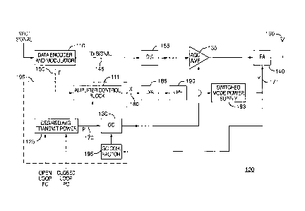
[0037] Reference is now made to the drawings. FIG. 1 illustrates a simplified
block diagram of a transmitter apparatus 100 in accordance with one example
embodiment. The transmitter 100 comprises a data encoder and modulator 110.
The
data encoder and modulator 110 converts an input signal, for example a digital
signal,
to be transmitted to the modulation technique appropriate to the air interface
standard in
which the mobile device is operating. In one embodiment, the data encoder and
-7-
CA 02740489 2011-05-17
modulator 110 uses CDMA modulation for use in an IS-2000 system. Other
modulation
schemes may include, without limitation, Universal Mobile Telecommunications
System
(UMTS), 802.11, Global System for Mobile Communications (GSM), Enhanced Data
rates for GSM Evolution (EDGE), Time division multiple access (TDMA), or
others that
are well known to those skilled in the art.
[0038] The data encoder and modulator 110 generates a Tx signal 145 and a
data format/data rate indicator that uniquely indicates a supported
combination of data
rate, coding and modulation method of the mobile device, referred to herein as
a data
indicator "r" 150. The Tx signal 145 comprises data frames to be transmitted
at variable
data formats or data rates. The data indicator "r" 150 indicates the variable
data rate
and format at which the signal is being transmitted. As will be explained in
more detail
below with reference to FIG. 2, in other embodiments, an explicit data rate
signal, such
as the data indicator "r" 150, need not be utilized. In such embodiments, one
or more
components of the transmitter can be appropriately calibrated so that data
rate and
format information is implicitly taken into account during operation of the
transmitter
100. Different settings or calibrations can be utilized for different data
rates, so that
during a data rate change the settings or calibrations corresponding to the
new data
rate can be selected. The data encoder and modulator 110 can be implemented
using
software, hardware or a combination of software and hardware.
[0039] The Tx signal 145, which can be a digital signal, is converted to an
analog
signal by a digital-to-analog converter 155 prior to performing analog
processing.
Analog processing can include, for example, mixing to an intermediate
frequency (IF)
and filtering, as well as any other necessary analog processes. In some
embodiments,
zero IF is used and mixing to an intermediate frequency is not required.
[0040] The amplitude of the analog processed signal is adjusted by an
automatic
gain control (AGC) amplifier 135. The signal can then be converted from an
intermediate frequency signal (or zero intermediate frequency signal) to an RF
frequency for transmission. Alternatively, the frequency conversion to an RF
frequency
is done before the AGC amplifier 135. Either way, the RF signal is input to an
RF power
amplifier 140 to generate a transmission signal, which is transmitted over the
air
-8-
CA 02740489 2011-05-17
interface by the antenna 160. In one embodiment, the AGC amplifier 135 and the
RF
power amplifier 140 can be included in an amplifier stage of the transmitter.
[0041] The data indicator "r" 150 is mapped by the first mapper 115 to
generate
signal PAPR(r) 165, which can be an effectively continuous signal. The signal
PAPR(r)
165 is the ratio of the peak signal power over the average signal power of Tx
signal 145
that corresponds to the data indicator "r" 150. This peak to average power
ratio signal is
designated as PAPR(r) 165. In one embodiment, PAPR(r) 165 is in dB or
proportional to
dB. In other embodiments, PAPR(r) can be scaled to any units that are suitable
for the
processor, hardware, or software as may be utilized in the particular
embodiment. The
first mapper 115 can be implemented using hardware, software (for example
using a
look-up table, an array of values or the like), or a combination of hardware
and software.
[0042] A desired average transmit power block 125 generates a desired average
transmit power indicator "p" 170. In some embodiments, the desired average
transmit
power block 125 uses one or more of an open loop power control method, a
closed loop
power control correction signal from the base station (e.g. transmitted every
1.25 ms),
and other base station parameters for the offset of power.
[0043] When operated using open loop power control, the desired average
transmit power block 125 can use the received total and pilot signal strengths
of a base
station signal received by the mobile device receiver and internal algorithms
to estimate
and adjust its own required transmit power. For example, if the received
signal strength
is high, then the desired average transmit power block 125 can determine that
a lower
transmit power may be sufficient. Likewise if the received signal strength is
low, the
desired average transmit power block 125 can determine that a larger transmit
power
may be required. Thus, a receiver (not shown) can be configured to receive
base station
signals and, based upon which, generate a received signal strength indicator
for the
desired average transmit power block 125.
[0044] For increased accuracy, the open loop transmit powers determined by the
average transmit power block 125 can further be adjusted, on a continuous
basis, using
closed loop power control commands transmitted by the base station to the
mobile
device receiver together with the received base station signals. These closed
loop
-9-
CA 02740489 2011-05-17
power control commands can instruct the desired average transmit power block
125 to
make incremental adjustments to the transmit power calculated based on the
received
signal strength indicator. For example, the commands can be to increase,
decrease or
maintain transmit power. Thus, the desired average transmit power block 125
can be
configured to receive the closed loop power control commands from the mobile
device
receiver as well. The average desired transmit power block 125 can be
implemented
using software, hardware or a combination of software and hardware.
[0045] Since the power control of the mobile device varies with time, the
desired
average transmit power indicator "p" 170 varies with time. In one embodiment,
such as
a cdma2000 mobile device, average transmit power indicator "p" 170 has units
of dBm
and is updated at the same rate as the closed loop power control (e.g., 1.25
ms). The
two signals, PAPR(r) 165 and desired average transmit power indicator "p" 170,
are
summed by a summer 175 that generates a peak power value in dBm (or
proportional
to it) representing the peak transmit power of the transmission signal
expected at
antenna 160, which is the RF counterpart of Tx signal 145 at baseband.
[0046] This peak transmit power is mapped by the second mapper 120 to an
effectively continuous "X" signal 180, whose value is effectively continuous
in a range
that the second mapper 120 is designed for. The generation of signal X 180 is
as
follows: for a given peak Tx power value, which is equal to p+PAPR(r),
determine the
corresponding optimal X signal 180 that gives the best transmitter power
efficiency
while still meeting the out of band spurious emissions and rho (waveform
quality)
requirements. An array of such values for the "X" signal 180 is stored in the
second
mapper 120. In one embodiment, this relationship is non-linear. Interpolation
may be
used in the mapping to get fine resolution and save storage memory. The array
of such
values for a transmitter may be determined by experimentation during
calibration and
testing of the transmitter. The second mapper 120, the summer 175, or both,
can be
implemented in hardware, software, or a combination of hardware and software.
The
first mapper 115, second mapper 120 and summer 175 may be included in an
amplifier
control block 111 of the transmitter (shown in FIG. 5), so that the amplifier
control block
111 is configured to generate an amplifier control signal for adjusting at
least one
parameter of the amplifier stage. For example, the first mapper 115 and second
mapper
-10-
CA 02740489 2011-05-17
120 can be used to determine the amplifier control signal based on peak to
average
power ratio and average transmit power of the RF transmission signal generated
by the
amplifier stage.
[0047] In some embodiments, one or more of the components of the transmitter
100, such as for example, data encoder and modulator 110, digital to analog
converter
155, AGC amplifier 135, can exhibit a stepped response during operation. For
example,
in some range of the respective input signal to the component, a small change
in the
input may cause a jump in the output. This can occur as a result of, for
example, but not
limited to, a stage bypass, a load switch, a quiescent current step, or a
quiescent
current ramp that results from the small change to the input signal. In some
embodiments, one or more of the mappers 115 and 120 may store more than one
array
or lookup table. The particular array or lookup table that is used in the
mappers 115 and
120 can depend on the input signal and the step response. For example, the
particular
array or lookup table used in the mappers 115 and 120 can be switched
synchronously
with the small change in the component input signal to anticipate the step
response.
Alternatively, instead of switching the array or lookup table, the mappers 115
and 120
can interpolate values falling between two different arrays or lookup tables.
Again this
can be performed synchronously with the small change in the component input
signal to
anticipate the step response. In this manner, one or more of mapper 115 and
mapper
120 can be used to compensate for the stepped response of the respective
component.
[0048] The "X" signal 180 is converted to an analog signal by a digital-to-
analog
(D/A) converter 185 and smoothed by a low pass filter LPF 190. The output of
the LPF
190 is used to adjust a setting of the RF power amplifier 140. In some
embodiments, the
RF power amplifier 140 includes or is otherwise coupled to a switched mode
power
supply and the setting adjusted by the "X" signal 180 is a supply voltage for
the RF
power amplifier 140, which can be generated using the switched mode power
supply in
response to the level of the "X" signal 180. Accordingly, the supply voltage
"Y" 171 is
supplied to a control input port of the RF power amplifier 140, and is
controllable in
terms of its magnitude. For example, the supply voltage "Y" 171 is lowered or
raised
accordingly for optimal power efficiency in generating the power of the
baseband Tx
signal 145 and its radio frequency counterpart, the transmission signal
radiated from
-11-
CA 02740489 2011-05-17
antenna 160. In some embodiments, the setting adjusted by the "X" signal 180
is a bias
(i.e. quiescent) current for the RF power amplifier 140, which can be
generated using
the switched mode power supply in a current mode.
[0049] The desired average transmit power indicator "p" 170 is also input to a
gain control block 130 to generate an automatic gain control signal for
controlling gain in
the AGC amplifier 135 based on the average transmit power of the Tx signal 145
once
amplified in the RF power amplifier 140. The gain control block 130 can be
implemented
using hardware, software (for example using a look-up table, an array of
values or the
like), or a combination of hardware and software.
[0050] The delay of the Tx signal 145 to the output of antenna 160 may be
designed to be the same as the delay from desired average transmit power
indicator "p"
170 or data indicator "r" 150 to the effects of "Y" 171 at antenna 160. When
these signal
delays are identical, the signals may be referred as being delay aligned.
Different
approaches to providing delay alignment can be utilized in different
embodiments. For
example, in some embodiments, "Y" 171 can be time-advanced relative to the Tx
signal
145 passing though D/A 185 and AGC amplifier 135. In some embodiments this can
be
done to compensate for the finite time required for the RF power amplifier 140
to move
its target outputs, for example when the supply voltage "Y" 171 is varied. In
some
embodiments, the delay alignment is implemented in software. In other
embodiments,
delay alignment can be implemented in hardware or a combination of hardware
and
software.
[0051] FIG. 1A illustrates an alternative embodiment of the transmitter
apparatus
100. In this embodiment, the arrangement and configuration of the first mapper
115, the
second mapper 120' and the summer 175 has been modified. The first mapper 115
remains coupled to the data encoder and modulator 110 to receive the data
indicator "r"
150 and generate a signal representative of peak to average power ratio.
However, the
second mapper 120' is coupled directly to the desired average transmit power
block 125
to receive the desired average transmit power indicator "p" 170 and generate a
signal
representative of average transmit power. The summer 175 is coupled to the
output of
-12-
CA 02740489 2011-05-17
the first mapper 115 and the second mapper 120', and generates "X" signal 180
to
control a parameter of the RF power amplifier 140.
[0052] In this embodiment, the first mapper 115, the second mapper 120', or
both
the first mapper 115 and the second mapper 120', can be re-written such that
the
influence of PAPR(r) 165 is introduced to "X" 180 at a different phase of the
amplifier
control block. For example, the second mapper 120' may be configured
specifically for
the current operating PAPR, in which case the influence of the first mapper
115 can be
correspondingly reduced. Second mapper 120' may include a plurality of
different stored
arrays or lookup tables corresponding to a plurality of different operating
PAPR, such
that a different "X" 180 signal is generated for each different operating PAPR
in the
plurality. Alternatively, the second mapper 120' may be configured as in FIG.
1, in which
case first mapper 115 can be modified to provide a correction factor for the
DC-DC
voltage, i.e. the supply voltage "Y" 171 of the RF power amplifier 140 (or
corresponding
amplifier control signal in either the analog or digital domain). In various
embodiments,
multiple amplifier control signals can be used. In some embodiments, the
amplifier
control signal can be or can control a bias current. In some embodiments, the
amplifier
control signal can be or can control a supply voltage. In some embodiments,
both a
supply voltage and a bias current can be used as amplifier control signals.
The one or
more amplifier control signals can be analog signals, digital signals or both
analog and
digital signals. As before, one or more of the first mapper 115, second mapper
120' and
summer 175, individually or in any combination thereof, can be implemented
using
hardware, software (for example using a look-up table, an array of values or
the like), or
a combination of hardware and software.
[0053] FIG. 2 illustrates an alternative embodiment of the transmitter
apparatus
100. In this embodiment, the first mapper 115 and the summer 175 of the
embodiment
described with reference to FIG. 1 are eliminated. The second mapper 120, with
adjustments to its stored array or lookup table, uses the desired average
transmit power
indicator "p" 170 as its input. In this case, the "X" signal 180 is determined
as follows: for
a given desired average transmit power indicator "p" 170, the corresponding
optimal "X"
signal 180 is generated that provides the best transmitter power efficiency
while
satisfying out of band spurious emissions and rho requirements. In other
words, the
-13-
CA 02740489 2011-05-17
second mapper 120 can store a plurality of array or lookup table values that
are specific
to a given data rate or operating PAPR, such that a different array or lookup
table is
selected and implemented for a corresponding different data rate (or PAPR,
which is
dependent on data rate). In this way, the second mapper 120 can generate the X
signal
180, as in the embodiments illustrated in FIGS. 1 and 1A, based on both peak
to
average power ratio and average transmit power, even though PAPR(r) 165 is not
specifically provided to the second mapper 120. Since PAPR can depend on data
rate,
by selecting a different array or lookup table to suit different PAPR, data
rate is implicitly
accounted for in the second mapper 120. As in the previous embodiments, the
values
that are stored (e.g. in software) in the arrays and look-up tables
implemented in second
mapper 120 may be determined experimentally as a way of calibrating the second
mapper 120 for optimal power efficiency.
[0054] The second mapper 120 may also be configured to generate signal "X"
180 so as to compensate for different environmental factors or conditions
(e.g.
temperature) in which the transmitter 100 is operating. For example, a
plurality of
different array or table values can be determined experimentally corresponding
to the
particular environmental condition. During operation of the transmitter 100,
that
environmental condition can be sensed and the appropriate array or look-up
table can
be loaded in the mapper 120. Additionally, or alternatively, the second mapper
120 can
be configured to compensate for prior knowledge of the transmitter operating
conditions
(e.g. frequency, drive band, etc), for example. In one embodiment, this is
done in the
digital domain. In variant embodiments, this can be done using analog methods,
or a
combination of digital and analog processing may be employed.
[0055] The stored array that is implemented by mapper 120 may be continuously
updated or substituted or interpolated at a rate appropriate to the changing
environmental or operating conditions (e.g. temperature drift, cell handoff,
data rate
change) of the transmitter 100. Accordingly, different suitable update rates
for the
second mapper 120 can be selected to fit the application or operating
condition.
Additional details pertaining to the embodiment described with reference to
FIG. 2 are
provided in the description above with respect to FIG. 1. In addition, as
mentioned
above, in various embodiments, multiple control signals can be used. In some
-14-
CA 02740489 2011-05-17
embodiments, the control signal can be or can control a bias current. In some
embodiments, the control signal can be or can control a supply voltage. In
some
embodiments, both a supply voltage and a bias current can be used as control
signals.
[0056] FIG. 3 illustrates another alternative embodiment of the transmitter
apparatus 100. This embodiment generates multiple "X" signals that are
provided to
adjust corresponding parts of the transmitter 100 or multiple parameters of
the same
part of the transmitter 100, instead of just one "X" signal 180 to adjust only
one
parameter of the power amplifier 140. The multiple "X" signals may be
implemented by
an array of second mappers 120 and 121, D/A converters 185 and 186, and low
pass
filters 190 and 191. Each individual element of "X" is determined as described
in the
above embodiment. For example, the multiple "X" signals can be generated to
provide
the best transmitter power efficiency while still satisfying out of band
spurious emissions
and rho requirements.
[0057] In the case where some elements of "X" signals are digital valued (High
or
Low), the corresponding mapper may be implemented as a threshold comparator.
The
multiple "X" signals may also include additional input variables such as the
transmitter
temperature and battery voltage. The second mapper 120 then becomes
multidimensional. Various simplified implementations (or approximations) of
multidimensional mapping tables may also be used.
[0058] The block diagram of FIG. 3 shows only two second mappers 120 and
121. However, the embodiments described herein are not limited to any
particular
number of second mappers 120. Further, the embodiments described herein are
not to
be limited to signal "X" 180 being an input to the RF power amplifier 140, and
instead
signal "X" 180 can be used as a control input for other components of
transmitter 100.
[0059] FIG. 3 illustrates an embodiment similar to FIG.1, but multiple "X"
signals
are illustrated in FIG. 3. The embodiments illustrated in FIGS. 1A and 2 can
similarly be
modified to generate multiple "X" signals. Therefore, in some embodiments, the
first
mapper 115 shown in FIG. 3 is optional and may be omitted, in which case the
second
mapper 120 can be configured, as described above with reference to FIG. 2, to
be
specific to a given data rate or operating PAPR. Environmental and operating
-15-
CA 02740489 2011-05-17
conditions, for example, can also be compensated using the second mapper 120
as
described above.
[0060] FIG. 3A illustrates an alternative embodiment of the transmitter
apparatus
100. In this embodiment, the transmitter 100 includes a gain control
compensation block
195 for generating a gain correction factor for the gain control block 130. As
shown in
FIG. 3A, the gain control compensation block 195 is coupled to the outputs of
LPF 190
and LPF 191 in a feedback loop with the gain control block 130. The gain
control
compensation block 195 compensates for gain expansion in the RF power
amplifier 140
due to variation of the supply voltage "Y" 171. For example, the gain control
compensation block 195 can predict the gain of the RF power amplifier 140
based on
the level of supply voltage "Y" 171 provided to the RF power amplifier 140.
The
relationship between these two quantities due to the power amplifier gain
expansion can
be either linear or non-linear. The gain control compensation block 195 can
then
generate a gain correction factor, which is used to adjust (e.g. reduce) gain
in the AGC
amplifier 135 by an amount appropriate to offset the gain expansion in the RF
power
amplifier 140 predicted for that level of supply voltage. In this way, the
output power of
the transmission signal generated by the RF power amplifier 140 can be
linearized with
respect to the gain of the AGC amplifier 135.
[0061] The gain correction factor can be fed back to the gain control block
130 in
different ways. For example, the gain correction factor can be introduced as
an
adjustment to the desired average transmit power indicator "p" 170, using a
summer
197 located upstream of the gain control block 130, to linearize the output of
the power
stage. Alternatively, the gain correction factor can be combined with the
automatic gain
control signal generated by the gain control block 130 in a summer 196 located
downstream of the gain control block 130. As a further alternative, the gain
correction
factor can be provided as an input to the gain control block 130, such that
the gain
control block 130 generates the automatic gain control signal based upon the
combination of the average desired transmit power indicator "p" 170 and the
gain
correction factor. The hashed lines in FIG. 3A represent these different
optional
configurations. Other configurations are possible. Also, gain correction as
described
herein can be performed in the analog domain, the digital domain or partially
in each
-16-
CA 02740489 2011-05-17
domain. Accordingly, one or more of the gain control compensation block 195
and
summers 196,197, individually or in any combination thereof, can be
implemented using
hardware, software (for example using a look-up table, an array of values or
the like), or
a combination of hardware and software.
[0062] FIG. 4 illustrates another alternative embodiment of the transmitter
apparatus 100. In this embodiment, the second mapper 120 is implemented by
suitable
analog hardware components and is included downstream of the D/A converter
185.
The functionality of the blocks remains otherwise as described herein, as does
operation of the remainder of the transmitter. The implementation of the
second mapper
120 has been changed in this embodiment.
[0063] FIG. 5 illustrates another alternative embodiment of the transmitter
apparatus 100. In this embodiment, the amplifier control block 111 is
explicitly illustrated
in the transmitter 100. The gain control compensation block 195 is also
illustrated. The
amplifier control block 111 receives the average transmit power indicator "p"
170 from
the desired average transmit power block 125 and, optionally, the data
indicator "r" 150
from the data encoder and modulator 110. Thus, in some embodiments the
amplifier
control block 111 is configured to receive both the average transmit power
indicator "p"
170 and the data indicator "r" 150, while in some other embodiments the
amplifier
control block 111 is configured to receive the average transmit power
indicator "p" 170
but not the data indicator "r" 150. The amplifier control block 111 generates
and
provides the "X" signal 180 to the D/A converter 185.
[0064] The amplifier control block 111 can comprise at least one mapper used
to
generate the "X" signal 180 based on the average transmit power indicator "p"
170.
Whether or not the data indicator "r" 150 is explicitly provided, the
amplifier control block
111 can further generate the "X" signal 180 based on a peak to average
transmit power
of the Tx signal 145. The transmitter apparatus illustrated in FIGS. 1, 1A, 2,
3 and 3A
depict some of the different possible embodiments of the amplifier control
block 111.
For example, FIGS. 1 and 1A illustrate embodiments in which the data indicator
"r" 150
is explicitly provided, while FIG. 2 illustrates embodiments where data rate
information
is accounted for implicitly within the configuration of the at least one
mapper included in
-17-
CA 02740489 2011-05-17
the amplifier control block 111. Moreover, FIGS. 3 and 3A illustrate
embodiments in
which multiple second mappers 120, 121 are incorporated to generate more than
control signal for the RF power amplifier 140. The amplifier control block 111
can be
implemented using hardware, software (for example using a look-up table, an
array of
values or the like), or a combination of hardware and software. For example,
the
amplifier control block 111 can be implemented on a programmable processing
device,
such as a microprocessor or microcontroller, Central Processing Unit (CPU),
Digital
Signal Processor (DSP), Field Programmable Gate Array (FPGA), general purpose
processor, and the like. The programmable processing device can be coupled to
program memory.
[0065] Switched mode power supply 193 is also shown explicitly in FIG. 5. In
this
example, the switched mode power supply 193 is coupled between the LPF 190 and
the
RF power amplifier 140, though the switched mode power supply 193 could be
included
at other locations or incorporated into other components within the
transmitter 100. The
switched mode power supply 193 can be, for example, a DC-DC converter or some
other voltage or current converter, which is configured to generate the supply
voltage
"Y" 171 in response to the "X" signal 180. Thus, the "X" signal 180 can be or
can specify
a pulse width or pulse density modulated signal, for example, to drive the
switched
mode power supply 193.
[0066] The amplifier control block 111 can be included within the control
system
199, which can form an integrated controller for the transmitter 100. As part
of such
integrated control, the control system 199 can generate hardware control
signals for one
or more of the physical components of the transmitter 100 based on one or more
input
signals, which can be provided by other components of the transmitter
apparatus. At
least one of the hardware control signals generated by the control system 199
can be
an amplifier control signal for adjusting at least one parameter of an
amplifier stage
included in the transmitter 100, such as the supply voltage or bias current of
the RF
power amplifier 140. Whether implemented using software or hardware or some
combination thereof, the control system 199 can generate the hardware control
signals
by defining a transfer function between the one or more input signals and the
one or
more control signals. In the example software implementation, the input-output
transfer
-18-
CA 02740489 2011-05-17
function can be defined by explicitly mapping input values to output values
and storing
that mapping in a lookup table or the like.
[0067] In some embodiments, the desired average transmit power block 125 can
also be included in the control system 199, in which case one or both of the
received
signal strength indicator and the closed loop power control commands can be
input
signals to the control system 199. In variant embodiments, the desired average
transmit
power block 125 can be provided separately from the control system 199 and the
average transmit power indicator "p" 170 can be provided as an input to the
control
system 199. In general, the one or more input signals provided to the control
system
199 can include at least one signal that is representative of the average
transmit power
of the Tx signal 145. The data indicator "r" 150 can also be provided as an
input signal,
in embodiments where the data indicator "r" 150 is explicitly available.
However, in
variant embodiments, data rate information may be embedded implicitly into the
one or
more mappers implemented in the amplifier control block 111, in which case the
data
indicator "r" 150 may not be an input signal to the control system 199 (hence
the
dashed line). But in general, the control system 199 can generate the hardware
control
signals based on a peak to average power ratio of the Tx signal 145, in
addition to the
average transmit power of the Tx signal 145, and regardless of the
availability of the
data indicator "r" 150.
[00681 In some embodiments, the gain control block 130 can also be included in
the control system 199. In these embodiments, the hardware control signals
generated
by the control system 199 can also include the automatic gain control signal
provided to
the AGC amplifier 135. To generate the automatic gain control signal, the
control
system 199 can further define an input-output transfer function between the
one or more
input signals and the automatic gain control signal. Alternatively the gain
control block
130 can be omitted from the control system 199 and implemented as a separate
hardware component in the transmitter 100. In these embodiments, if the
desired
average transmit power block 125 is included in the control system 199, then
the
average transmit power indicator "p" 170 can be outputted from the control
system 199
and provided to the gain control block 130.
-19-
CA 02740489 2011-05-17
[0069] In some embodiments, the gain control compensation block 195 can also
be included in the control system 199. In these embodiments, the voltage
supply signal
"Y" 171 can be one of the input signals to the control system 199, and the
input-output
transfer function for the automatic gain control signal can be further defined
in terms of
the voltage supply signal "Y" 171. Alternatively, some other signal generated
internally
within the control system 199, such as the signal "X" 180, which is
representative of the
power amplifier supply voltage can be used to adjust the automatic gain
control signal.
As described herein, the adjustment can be performed to compensate for gain
expansion in the RF power amplifier 140 when the supply voltage is varied.
Alternatively, the gain control compensation block 195 can be omitted from the
control
system 199 and implemented as a separate hardware component in the transmitter
100.
[0070] Regardless of what elements of the transmitter 100 are included, the
control system 199 can be implemented on one or more programmable processing
devices, such as a microprocessor or microcontroller, Central Processing Unit
(CPU),
Digital Signal Processor (DSP), Field Programmable Gate Array (FPGA), general
purpose processor, and the like. The programmable processing device can be
coupled
to program memory for implementing the functions of the control system 199,
and can
have suitably configured input and output terminals or circuits for
interfacing with the
various hardware components of the transmitter 100 that are controlled using
the
programmable processing device.
[0071] FIG. 6 illustrates acts of a method 200 for optimizing power efficiency
in a
transmitter apparatus in accordance with at least one embodiment. Some acts of
the
method 200 can be performed using hardware components, while other acts of the
method 200 can be performed using software components. Some acts of the method
200 can be performed using both hardware and software components. Some acts of
the
method 200 can be performed alternatively using either hardware or software
components, as will be described. Accordingly, the method 200 can be performed
using
software components only, hardware components only, or a combination of
software
and hardware components.
-20-
CA 02740489 2011-05-17
[0072] At 205, an encoded and modulated transmit signal based on an input
signal is generated. The input signal can be a digital communication signal,
such as a
digitized voice signal or data signal, which is to be transmitted. The input
signal can be
encoded and modulated using a communication standard employed by the
transmitter.
As a non-limiting example, the modulation scheme used can be the CDMA
modulation
scheme, but could also be UMTS, GSM, EDGE, TDMA, or some other scheme. The
encoding and modulating can be performed using hardware components, but could
also
be performed in software or some combination of the two.
[0073] At 210, an analog representation of the encoded and transmitted signal
is
generated. A suitably configured digital to analog converter can be used, for
example.
[0074] At 215, the analog representation of the encoded and modulated transmit
signal is amplified in an amplifier stage to generate a transmission signal.
For example,
the amplifier stage can include an automatic gain control amplifier (e.g. 135
in FIG. 1)
and an RF power amplifier (e.g. 140 in FIG. 1). This act can further comprise
filtering
and mixing the analog representation of the encoded and modulated signal with
an
intermediate frequency, prior to amplification in the amplifier stage.
[0075] At 220, an amplifier control signal is generated based on a peak to
average power ratio and an average transmit power of the transmission signal.
Various
approaches can be followed in order to generate the amplifier control signal.
As one
example, a type of the encoded and modulated transmit signal can be mapped,
using a
first mapping function, to a first signal representation of the peak to
average power ratio,
and a second signal representative of the average transmit power of the
transmission
signal can be generated using a second mapper. The first and second signals
can then
be summed together to generate the amplifier control signal.
[0076] Alternatively, a plurality of different mapping functions can be used,
each
mapping function corresponding to a different peak to average power ratio of
the
transmission signal, to generate the amplifier control signal. Accordingly,
the desired
average power of the transmission signal supplemented implicitly with peak to
average
power ratio information of the transmission signal (e.g. through selection of
a given
mapping function) can be mapped into the amplifier control signal.
-21-
CA 02740489 2011-05-17
[0077] The act at 220 can further comprise generating the amplifier control
signal
based on one or more environmental conditions in which the transmitter is
operating,
such as temperature, as well as one or more operating conditions of the
transmitter,
such as transmit frequency and drive band.
[0078] The act at 220 can be performed using one or more transistor logic
circuits, one or more software components, comprising instructions executable
by a
processor and storable in memory for example, or some combination of hardware
and
software components.
[0079] At 225, at least one parameter of the amplifier stage is adjusted using
the
amplifier control signal. For example, the amplifier control signal can be or
can control a
supply voltage of the RF power amplifier, and can be generated at 220 so that
the RF
power amplifier operates efficiently while satisfying out of band and rho
requirements.
[0080] Although not expressly illustrated in FIG. 6, the method 200 can
further
comprise generating an automatic gain control signal for controlling gain in
the
automatic gain control amplifier, which can be included in the amplifier stage
in variant
embodiments. The automatic gain control signal can be generated based on the
average transmit power of the transmission signal. Moreover, the method can
further
comprise generating a gain correction factor based on the amplifier control
signal, which
is used to adjust the automatic gain control signal to compensate, as an
example, for
gain expansion in the RF power amplifier due to bias point variation.
[0081] It should be appreciated that in some embodiments, the method 200 can
comprise still further acts not explicitly shown in FIG. 6, while in other
embodiments one
or more of the acts illustrated may be omitted or performed in a different
order than as
illustrated.
[0082] FIG. 7 illustrates acts of a method 250 for optimizing power efficiency
in a
transmitter apparatus in accordance with at least one embodiment. Like method
200
shown in FIG. 6, the acts of the method 250 can be performed using hardware
components, software components or a combination of hardware and software.
Accordingly, the method 250 can also be performed using software components
only,
hardware components only, or a combination of software and hardware
components.
-22-
CA 02740489 2011-05-17
[0083] At 255, an encoded and modulated transmit signal is generated in a
transmitter apparatus based on a digital input signal to be transmitted. The
input signal
can be encoded and modulated using a communication standard employed by the
transmitter. As a non-limiting example, the modulation scheme used can be the
CDMA
modulation scheme, but could also be UMTS, GSM, EDGE, TDMA, or some other
scheme. A data indicator corresponding to the encoded and modulated signal is
also
generated.
[0084] At 260, the encoded and modulated signal is converted into an analog
transmission signal. For example, a suitably configured digital to analog
converter can
be used.
[0085] At 265, an output peak to average power ratio signal value is selected
from an array of different possible peak to average power ratio signal values.
Each
different peak to average power ratio signal values can correspond to a
different data
rate or data format, and the output peak to average power ratio signal value
can be
selected corresponding to the data indicator generated at 255. Thus, the
output peak to
average power ratio signal value generated at 265 can reflect the data rate or
data
format of the input digital signal.
[0086] At 270, a desired transmit power level signal value can be generated.
For
example, the desired average transmit power block 125 (illustrated in FIG. 1)
operating
in closed or open loop mode can be used to generate the desired transmit power
level
signal. Accordingly, one or more of a received signal strength indicator and
closed loop
power control commands can be used.
[0087] At 275, an automatic gain control signal is generated based on the
desired
transmit power level signal value. The automatic gain control signal can be
generated,
for example, so that the signal amplification provided by an automatic gain
control
amplifier (see e.g. 135 in FIG. 1) included in the transmitter apparatus
causes a
transmission signal to be generated at the desired average transmit power
level.
[0088] At 280, the desired transmit power level signal value and the peak to
average power ratio signal value can be added together to generate a peak
transmit
power level signal value.
-23-
CA 02740489 2011-05-17
[0089] At 285, the value of the peak transmit power level signal value can be
mapped, essentially continuously, to a value for at least one control signal
for at least
one control device or element included in the transmitter apparatus. For
example, the
control device can be a switched mode power supply (see e.g. 193 in FIG. 5)
that
controls a supply voltage for an RF power amplifier (see e.g. 140 in FIG. 1)
included in
the transmitter apparatus. The control values for the switched mode power
supply can
be continuously mapped to achieve an optimized power efficiency in the RF
power
amplifier of the transmitter apparatus, while still meeting out of band
spurious emissions
and waveform quality requirements. This can be accomplished by ensuring that
the
supply voltage for the RF power amplifier is large enough to accommodate the
peak
transmit power level of the transmission signal with sufficient headroom.
[0090] At 290, if the control value generated at 285 is a digital signal, the
control
signal can be converted to an analog signal prior to being input into the
control device.
Alternatively, if the control value generated at 285 is already an analog
signal, 290 can
be omitted from the method 250.
[0091] FIG. 8 illustrates acts of a method 300 for optimizing power efficiency
in a
transmitter apparatus in accordance with at least one embodiment. Method 300
can be
performed entirely using software components. Some hardware components may be
utilized as well, in variant embodiments.
[0092] At 305, a signal representative of an average transmit power of a
transmission signal is received. For example, the representative signal can be
provided
to an input terminal of a processor.
[0093] At 310, an amplifier control signal is determined by mapping the
average
transmit power and a peak to average power ratio of the transmission signal to
a control
value for an amplifier stage, which can include an automatic gain control
amplifier (see
e.g. 135 in FIG. 5) and an RF power amplifier (see e.g. 140 in FIG. 5). The
mapping can
be encoded in one or more lookup tables or the like, implemented in memory
coupled to
the processor. The average power ratio of the transmission signal can be
embedded
within the one or more lookup tables, for example, in the case where a
different lookup
table is implemented for each of a number of different possible average power
ratios.
-24-
CA 02740489 2011-05-17
Alternatively, a signal representative of an average power ratio can be
received, for
example, at a second input terminal of the processor, and then used to modify
values
stored in the one or more lookup tables according to the average power ratio
of the
transmission signal.
[0094] At 315, the amplifier control signal generated at 310 is provided to
the
amplifier stage to adjust at least one parameter of the amplifier stage
according to the
control value. For example, an output terminal of the processor can carry the
amplifier
control signal to the amplifier stage or, perhaps, some other element coupled
intermediately between the processor and the amplifier stage. In some
embodiments,
the amplifier control signal can be provided to a switched mode power supply
coupled to
the RF power amplifier, and the value of the amplifier control signal can
specify a supply
voltage for the RF power amplifier.
[0095] In some of the herein described embodiments, signals X may control
various devices within the transmitter, including one or more power
amplifiers, one or
more stages of a power amplifier, one or more drive amplifiers, one or more
AGC
amplifiers, one or more power supplies for a power amplifier and/or other
devices in a
transmitter, one or more power supplies for other devices on components, one
or more
mixers, one or more matching networks, one or more filters, one or more power
couplers or switches, one or more charging circuits, one or more voltage or
current
sources, one or more voltage or current regulators, one or more voltage or
current
converters, and any combination of these components.
[0096] In still other embodiments, inputs such as the multiple X signals, to
control
certain transmitter circuit parameters may include (but are not limited to):
(a) bias to
each or some of the amplifying devices inside a power amplifier so that only
the
minimum bias is provided to obtain the required out of band spurious emissions
and rho
for each given transmitted power and/or PAPR values in the supported range;
(b) power
supply voltage(s) to all or selected stages of an RF power amplifier and/or
other circuits
in the transmitter apparatus; such power supply voltages are supplied to the
circuits so
that only the minimum voltage is provided to obtain the required out of band
spurious
emissions and rho for each given transmitted power and/or PAPR values in the
-25-
CA 02740489 2011-05-17
supported range; (c) to switch in or out, or turn on or off selected stages
according to
the transmitted power and/or PAPR values; and (d) gains of all or selected
components
of the amplifier stage in the transmitter; (e) conducting angle of all or
selected
components of the amplifier stage in the transmitter; (f) class of amplifying
(e.g., Class
A, AB, C, D, ...) of all or selected components of the amplifier stage in the
transmitter;
(g) load or impedance of all or selected components of the amplifier stage in
the
transmitter; (h) a gain distribution; or (i) a combination of any or all of
(a), (b), (c), (d),
(e), (f), (g) and (h).
[0097] At least some of the embodiments of the transmitter apparatus and power
optimization method described herein provide improved power efficiency of
transmitters
having varying transmit power and high/variable PAPR. This may, for example,
provide
a mobile, battery-powered device with increased battery life performance.
[0098] A number of embodiments have been described herein. However, it will
be understood by persons skilled in the art that other variants and
modifications may be
made without departing from the scope of the embodiments as defined in the
claims
appended hereto.
-26-