Note: Descriptions are shown in the official language in which they were submitted.
CA 02740681 2011-05-19
244757-2
BUSBAR ELECTRICAL POWER CONNECTOR
FIELD OF THE INVENTION
The present invention is related to power connectors. In particular, the
present
invention is related to a dual pole power connector for enabling a power
connection to
dual pole parallel power busbars.
BACKGROUND OF THE INVENTION
Transmission of power through an electric circuit results in energy losses. In
circuits
where the voltage does not remain constant, such losses may be the result of
many
factors, including conductive losses as well as losses associated with a
voltage that
changes, such as inductive losses and capacitive losses. Conductive losses
include
heat loss resulting from resistance of the conductors and electrical
connectors between
conductors. Inductive losses may be proportional to a frequency of voltage
change
and a circuit's inductance, and/or a speed of a voltage change and the
circuit's
inductance. A circuit's inductance may be influenced by the geometry of the
circuit
itself, or the geometry of the electrical connector itself.
The nature of power transmitted through electric circuits is continuously
changing.
For example, in switched circuits, the speed at which a voltage may change is
constantly increasing with the onset of new more advanced high switching speed
semiconductors. This is a consequence of the new semiconductor technology and
the
need to obtain high power density in electronic circuits. Consequently,
because
inductive losses are proportional to a speed of a voltage change, and are
related to the
geometry of the circuit, increased attention must be paid to the geometry of
electrical
connectors in order to minimize inductive losses. Thus, there remains room in
the art
for improvement.
BRIEF DESCRIPTION OF THE INVENTION
An embodiment is directed toward a dual pole busbar power connector including
opposing elements configured to form a slot configured to receive a dual-pole
blade
1
CA 02740681 2011-05-19
244757-2
therebetween. The slot extends from busbars to opposing element distal ends.
The
opposing elements each includes: a first contact extending into the slot from
the
opposing element; and a second contact extending into the slot from the
opposing
element and disposed farther from a slot busbar end than the first contact.
When the
dual-pole blade is fully inserted in the slot the first contact mates a
respective blade
element at a location in the slot more proximate the slot busbar end than a
slot distal
end.
Another embodiment is directed toward a dual pole electrical connector
including: at
least one electrically conductive element for each busbar of a dual parallel
busbar
power conversion equipment, the electrically conductive element including a
first
contact, wherein when a dual-pole blade is inserted into the dual pole
electrical
connector the first contact electrically connects a respective busbar to a
respective
blade element via a first element first contact path. The first element first
contact
paths of respective poles form a loop comprising an region therebetween
comprising a
cross section, and a dual pole electrical connector inductance is influenced
by a size of
the cross section, and the cross section is configured by the first contact
paths to keep
the dual pole electrical connector inductance below seven nanohenries.
BRIEF DESCRIPTION OF THE DRAWINGS
The invention is explained in the following description in view of the
drawings that
show:
FIG. 1 shows a cross section of a side view of an electrical connector.
FIG. 2 shows a perspective view of a blade commonly used with the electrical
connector of FIG. 1.
FIG. 3 shows a cross section of a side view of the electrical connector of
FIG. 1 with
the blade of FIG. 2 inserted.
FIG. 4 is a close up of a portion of FIG. 3.
FIG. 5 schematically shows a current path through the connector of FIG. 1.
2
CA 02740681 2011-05-19
244757-2
FIG. 6 schematically shows the current loop of FIG. 5 and a cross section of
the
region bounded by the current path.
FIG. 7 schematically shows an alternate current loop and a cross section of
the region
bounded by the current loop.
FIG. 8 shows a cross section of a side view and current path of another
embodiment
of an electrical connector.
FIG. 9 schematically shows the current path of FIG. 8 and a cross section of
the
region bounded by the current path.
DETAILED DESCRIPTION OF THE INVENTION
New semiconductor technologies are capable of providing much faster switching
than
has been seen in the art. Specifically, when a voltage is changed from a first
voltage
to a second voltage the change ideally would be instantaneous. Were this
signal
profile depicted on a graph with voltage on the y-axis and time on the x-axis,
the line
representing the voltage would, ideally, be vertical when the voltage changed.
This
line, i.e. the signal edge, however, is not vertical, and historically this
has been the
result of the switching technology. However, with the advent of switching
technology
using silicon carbide, for example, the switching equipment is capable of much
faster
transitions, i.e. the signal edge slope is significantly steeper. However when
the new
switching technology was used with conventional circuit hardware, including
the
electrical connectors, the expected increased efficiency of the relatively
"faster edge"
was not realized to its potential. Upon initial investigation it was
discovered that
efficiency gains realized by the faster edge were being offset by increased
losses in
the conventional circuit hardware associated with that same faster edge. Upon
further
investigation, it was discovered that certain prevalent conventional
connectors, such
as Tyco/Elcon "Crown Clip" connectors, as well as Anderson Power Products
"Power
Clip" connectors, possess certain geometries. Without being bound by any
particular
theory, it is believed that this geometry, which may best be considered a
"loop" in
terms of its contribution to the total inductance of the electrical connector,
causes
electrical losses in the circuit because it resists the change of faster edge
switching.
3
CA 02740681 2011-05-19
244757-2
The inductance of the geometry has been present even with relatively slow edge
switching, but the losses were negligible because the transition was slower.
However,
as the edge speed increases the losses are no longer negligible. The
identified
geometry is like a loop in the traditional sense of the term, where one may
envision a
coiled wire, and thus identification of the inductance inducing geometry was a
significant step in itself.
In addition, with the advent of the "faster edges," switching frequencies
themselves
can in turn be increased. For example, frequencies of 10kHz have been possible
with
relatively slower edge technologies. However, switching equipment had been the
limiting factor because that technology had a relatively long transition time
(edge)
between the first and second voltages. However, with the advent of the new
switching technologies, the switching equipment was not the limiting factor
anymore,
but as described above, the hardware had become the limiting factor. However,
the
demand for higher switching speed remains, and thus the recognition of the
conventional geometry and innovative new design will permit switching speeds
to
increase in excess of 500kHz, making the resulting geometry, although
seemingly
simple, critical for technological advancement.
Inductance resulting from loops in an electrical circuit, i.e. a signal path,
can be
modeled with various known equations, but in general terms if one wants to
reduce or
eliminate a loop one can reduce a cross sectional of a region bound by the
conductor(s) that form the loop (i.e. the cross section). As a result, the
inventors have
devised a power connector that significantly changes the current flow path
geometry
present in connectors of earlier designs, minimizing the region, and hence the
cross
section of the region, bounded by the conductors forming the loop. They have
done
this by adding an electrical contact at a point close to the busbar. The
relevance of the
contact, it is believed, is that its location is specifically chosen to reduce
the cross
section of the region bound by the newly identified inductance causing loop.
The connector described below is suited for making an electrical connection
between
parallel busbars, each busbar being part of a single circuit, and a blade that
is inserted
into a slot in the connector, shown later. Thus, as used herein, a dual pole
connector
4
CA 02740681 2011-05-19
244757-2
is a connector used to establish electrical communication between at least two
busbars
of a single circuit, and a component to be run off that circuit, where circuit
comprises
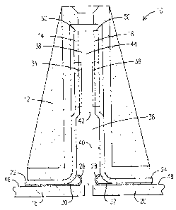
a first busbar, the component, and a second busbar. Turning to the drawings,
FIG. 1
shows a side view of a dual pole busbar power connector ("connector") 10. The
connector has a housing 12 to hold two opposing elements, first element 14 and
second element 16. In an embodiment these are electrically connected to first
busbar
18, which serves as one pole of a circuit, and second busbar 20, which serves
as a
second pole of a circuit, respectively, via first element flanged end 22 and
second
element flanged end 24. However, this electrical connection may be made in any
manner known to those of ordinary skill in the art. First element 14 may
include first
element first contact 26, and second element 16 may include second element
first
contact 28. In an embodiment, first element first contact 26 may be in
electrical
communication with first busbar 18 via a first element first contact plate 30,
and
second pole first contacts may be in electrical communication with a second
busbar 20
via a second element first contact plate 32. However, again, electrical
communication
between the first contacts and the busbars may be made in any manner known to
those
of ordinary skill in the art. In an embodiment, first element first contact 26
and
second element first contact 28 may be resilient and may oppose each other.
First
element 14 may include first element second contact 34, and second element 16
may
include second element second contact 36. These second contacts may be
resilient
and may oppose each other. Any contacts in the embodiments may also include a
plurality of contacts, or a line or plane of contact, and may extend across a
width of
the any surface they are intended to contact. It can be seen that a slot 38 is
formed
between the first element 14 and second element 16. In an embodiment it can
also be
seen that a distance 40 between first element 14 and second element 16 at the
first
contacts 26, 28 is greater than a distance 42 between first element 14 and
second
element 16 at the second contacts 34, 36. Slot 38 has slot length 44, which is
a
distance from first busbar surface 46 and second busbar surface 48 to distal
ends 50 of
the first element 14 and second element 16.
A dual pole blade 52 as shown in FIG. 2 is inserted into slot 38. Dual pole
blade 52
may include a first blade element 54 and a second blade element 56 separated
by an
CA 02740681 2011-05-19
244757-2
insulator 58. First blade element 54 includes first blade element tip 60 and
second
blade element 56 includes second blade element tip 62, which is the portion of
the
dual pole blade that is first inserted into slot 38 and when fully inserted
rests closest to
the first busbar 18 and second busbar 20.
FIG. 3 shows the dual pole blade 52 inserted into the connector 10. It can be
seen in
an embodiment that first element first contact 26 contacts the first blade
element 54 at
first blade element tip 60, and second element first contact 28 contacts
second blade
element 56 at second blade element tip 62. First element second contact 34
contact
first blade element 54 at a location farther from the busbars, and likewise
second
element second contacts 36 contact the second blade element 56 at a location
farther
from the busbars. As can be seen in FIG. 4, which is an amplified view of
first
element first contact 26 and second element first contact 28, cross section 64
of the
region bounded in part by a first element first contact path 66 and a second
element
first contact path 68. Also seen is the first element first contact path 66,
which is the
path from the first element first contact 28 where it contacts the first
busbar 18,
through the first element first contact 26, to where the first element first
contact 26
makes contact with the first blade element 54. Similarly, the second element
first
contact path 68 is the path from the second element first contact 28 where it
contacts
the second busbar 20, through the second element first contact 28, to where
the
second element first contact 28 makes contact with the second blade element
56.
Thus, as can be seen in FIG. 5, the identified geometry, loop 70, follows the
current
path from the first busbar 18, through the first element first contact 26, up
the first
blade element 54, returning down the second blade element 56, through the
second
element first contact 28, to the second busbar 20.
FIG. 6 a schematic of the shape of first contact loop 70 of FIG. 4, showing
cross
section 64, and second cross section 72. Second cross section 72 is shown to
illustrate
the concept, because there is a region, albeit very small, between the first
blade
element 54 and the second blade element 56. However, second cross section 72
is
small relative to cross section 64, and its contribution to the inductance of
the
connector is relatively negligible. Further, it is relatively difficult to
eliminate this
6
CA 02740681 2011-05-19
244757-2
region due to the electrical need to keep the first blade element 54 and the
second
blade element 56 electrically isolated. As a result, the cross section 64
receiving
attention can be described as a cross section of the region bound by the first
element
first contact path 66 and the second element first contact path 68.
In the embodiment shown in FIG 6, cross section 64 has already been configured
to
be as small as possible because the first element first contact path 66 and
the second
element first contact path 68 are as short as possible, and are also close
together.
Either of these factors can be used to sufficiently reduce the cross section,
and in this
embodiment both are used for maximum benefit. It is this configuration, which
has
the most minimized cross section 64, which permits the relatively fast edge
signals to
propagate through the connector with the least limiting inductance.
By way of comparison to FIG. 6, shown in FIG. 7 is second contact loop 74 that
current would travel along if first element first contact 26 and second
element first
contact 28 were not present. In that case electrical communication with the
first blade
element 54 and a second blade element 56 would be through the first element
second
contact 34 the second element second contacts 36 respectively, which results
in
second contact loop 74. As shown in FIG. 7 when compared to FIG. 6, the cross
section 76 bounded by this second contact loop 74, i.e. this geometry, is much
larger,
and consequently would have a much larger inductance relative to the geometry
of
FIG. 5.
The inventors have found that connectors with contact paths similar to that of
FIG 7
have inductance of seven nanohenries and above. They have also found that
connectors with geometries similar to that of FIG 5 have inductance of below
seven
nanohenries. In certain embodiments, such as those shown in FIG. 5, these
connectors have inductances of 1 to 1.5 nanohenries. Any reduction in the
cross
section of the region bounded by the current path over that of other
configurations
will correspond to a reduction in the inductance, and therefore any reduction
in cross
section is an improvement. Thus, it can be seen that the geometry disclosed in
FIG. 1
is a significant improvement over other geometries used in the art.
7
CA 02740681 2012-11-29
244757
In an alternate embodiment shown in FIG. 8, connector 10 has first element 78
and
second element 80. Each in turn has first element first contact 82 and second
element
first contact 84 respectively. The loop 86 that the current would follow
through this
embodiment would be similar to the other loops. As shown in FIG. 9, the cross
section 88 bounded by the geometry is a little larger than that shown in the
embodiment of FIG. 5, but still less than that shown in FIG. 7, and thus an
advantage
is still realized over other configurations. Various other configurations are
envisioned
to be within the scope of this disclosure, so long as those configurations
reduce the
cross section of the region bounded by the current path below that of the
other
configurations. It is further noted that some of the current may flow through
the
second contacts of the connectors, and thus not all the current will be
subject to the
improved geometry, but enough of the current will follow the improved current
paths
that the above described improvements will be realized. Other considerations
may
require the presence of the second contacts, such as stabilizing the blade, or
increasing
contact area in order to maximize current flow capacity, and thus they have
not
necessarily been eliminated from every embodiment. Conversely, they may not be
present in an embodiment where their presence is not needed.
While various embodiments of the present invention have been shown and
described
herein, it will be apparent that such embodiments are provided by way of
example
only. Numerous variations, changes and substitutions may be made without
departing
from the invention herein.
8