Note: Descriptions are shown in the official language in which they were submitted.
= CA 02740942 2013-01-08
=
WO 2010/060511 1 PCT/EP2009/007651
=
Plug-in connector for printed circuit boards
The present invention relates to a multiple plug-in
connector for printed circuit boards for fastening to a
printed circuit board, having a mounting part and having at
least two contact sections which each have a plug-in part
for connection by plugging-in to a complementary mating
part of a plug-in connector, an opening being formed for
each contact section in the mounting part and each contact
section passing through one of the openings by its plug-in
part and being fastened to the mounting part mechanically,
each contact section having, on a side adjacent the printed
circuit board, at least one contact member for making
electrical contact with a conductor on the printed circuit
is board.
The invention also relates to a printed circuit
board having an electronic circuit and having a multiple
plug-in connector for printed circuit boards which is
arranged on the printed circuit board and which is
electrically connected to the electronic circuit.
Known from DE 43 12 091 Al is a plug-in connector for
printed circuit boards which has a slotted opening, thus
enabling a flat, planar region of a printed circuit board,
which carries conductors, to be inserted in this opening.
Extending along the region carrying the conductors are a
plurality of parallel conductors which come from a printed
circuit on the printed circuit board.
Known from DE 197 20 678 Cl is a RF co-axial plug-in
connector part for mounting in a fixed position on a
printed circuit board. Arranged on a metal housing of the
RF co-axial plug-in connector part are solder pins and a
metal plug-in part in the form of, as the case may be, a
CA 02740942 2011-04-13
WO 2010/060511 2 PCT/EP2009/007651
co-axial plug or co-axial socket. When the housing is
. fitted down onto a printed circuit board by its underside,
the solder pins engage in electrical connections associated
with them on the printed circuit board, these electrical
connections taking the form of contact-making mounting
holes into which the solder pins are soldered. To enable a
plurality of such RF co-axial plug-in connector parts to be
incorporated into a component, there is known from DE 198
05 944 Cl a connector strip which has a plurality of
lo receiving openings. Angled co-axial plug-in connectors are
inserted in respective ones of the receiving openings by
their plug-in parts and are held mounted by the connector
strip. The RF plug-in connectors are usually first inserted
in the connector strip and the connector strip is then
fitted down on the printed circuit board, thus causing the
solder pins of all the RF plug-in connectors to engage in
corresponding mounting holes in the printed circuit board
and causing soldering faces on all the RF plug-in
connectors to be arranged against corresponding solder pads
on the printed circuit board. However, a problem arises in
this case, which is that the solder pins of the plurality
of RF plug-in connectors mounted in the connector strip
have to be aligned in exact positions so that they will
engage in their respective mounting holes simultaneously
when the connector strip is fitted down. At the soldering
faces on the plurality of RF plug-in connectors mounted in
the connector strip, the additional problem arises that
these need to be arranged not only in an exact position but
also as exactly as possible in the plane of the printed
circuit board. This makes the fitting of the RF plug-in
connectors to the connector strip time-consuming and cost-
intensive.
CA 02740942 2012-09-10
WO 2010/060511 3 PCT/EP2009/007651
The object underlying the invention is to simplify a
multiple plug-in connector for printed circuit boards of
the above kind and a printed circuit board of the above
kind with regard to the fitting process and at the same
time to improve their electrical characteristics.
This object is achieved in accordance with the
invention by a multiple plug-in connector for printed
circuit boards of the above and by a printed circuit board
of the above kind. Advantageous embodiments of the
lo invention are described in the other claims.
In a multiple plug-in connector for printed circuit
boards of the above kind, provision is made in accordance
with the invention for the mounting part to have at least
one first contact device which is so arranged and formed
that the said first contact device makes electrical contact
with at least one contact member of a contact section, the
mounting part having at least one second contact device
which is electrically connected to at least one first
connecting means and which is designed to make electrical
contact with a conductor on the printed circuit board.
This has the advantage that the function by which the
contact section makes electrical and mechanical contact
with the printed circuit board is decoupled from the
contact members of the contact section, thus making the
plugging-in function and the making of electrical contact
functionally separate from one another. In this way, the
requirement for contacts which are to be electrically
connected to the printed circuit board to be exactly
positioned is shifted to the mounting part, where it is
easier to satisfy than at the contact members of the
CA 02740942 2011-04-13
WO 2010/060511 4 PCT/EP2009/007651
contact sections. In other words, the mounting part makes
electrical contact between a contact member of a contact
section and a conductor on the printed circuit board, which
means that there is no longer any need for direct
electrical contact to be made between the said contact
member of the contact section and the conductor on the
printed circuit board. Exact positioning of this contact
member of the contact section is no longer necessary,
because the function of making electrical contact for this
one contact element or the plurality of contact elements is
taken over by the mounting part.
The second contact device of the mounting part is
usefully so arranged and formed that the said second
contact device makes electrical contact with that conductor
on the printed circuit board which has to be electrically
connected to that contact member of the contact section
which is electrically connected to that first contact
device which is electrically connected to the said second
contact device.
In a preferred embodiment, the contact section takes
the form of an RF plug-in connector having an outer
conductor and a centre conductor, at least one contact
member of the contact section taking the form of an outer-
conductor contact and at least one other contact member of
the contact section taking the form of a centre-conductor
contact. In this case, the first contact device of the
mounting part is preferably electrically connected to all
the outer-conductor contacts of the contact sections and
the second contact device, which is electrically connected
to the first contact device, is designed to make electrical
contact with an outer conductor, i.e. an earth conductor,
on the printed circuit board.
CA 02740942 2011-04-13
WO 2010/060511 5 PCT/EP2009/007651
Manufacture and assembly which are particularly easy
and inexpensive with, at the same time, a standard of
contact for radio-frequency applications which is high and
reliably repeatable can be achieved by having the first
s contact device take the form of a clamped contact.
Electrical contact of a particularly high standard can be
achieved by coating the contact areas of the clamped
contact with nickel.
Defined and locally confined points of contact between
the conductors on the printed circuit board and the second
contact device of the mounting part and a corresponding
predetermined path of flow for a flow of current are
obtained by causing the second contact device of the
mounting part to have a plurality of individual elevations
which are formed on the side of the mounting part adjacent
the printed circuit board in such a way as to be spaced
apart from one another.
Contact areas between the mounting part and the
printed circuit board which can be soldered particularly
well are obtained by causing contact areas of the second
contact device of the mounting part to have a finish of
tin.
In a preferred embodiment, the mounting part takes the
form of a stamped/punched and bent part.
In an alternative embodiment, the mounting part takes
the form of a zinc die casting.
The first and/or second contact devices of the
mounting part are usefully formed in one piece with the
mounting part.
In a preferred embodiment, the mounting part has, on a
side adjacent the printed circuit board, at least one pin
which projects from this side, to engage in a corresponding
mounting opening in the printed circuit board and to make a
CA 02740942 2011-04-13
WO 2010/060511 6 PCT/EP2009/007651
mechanical and/or electrical connection to the printed
circuit board.
To secure the mounting part mechanically to the
printed circuit board to an additional degree, the mounting
part has a fastening portion to connect the mounting part
mechanically to the printed circuit board. The fastening
portion has for example an opening which is designed to
have a screw screwed into the printed circuit board pass
through it.
In a printed circuit board of the above kind,
provision is made in accordance with the invention for the
multiple plug-in connector for printed circuit boards to be
designed as described above.
This has the advantage that the function by which the
contact section makes electrical and mechanical contact
with the printed circuit board is decoupled from the
contact members of the contact section, thus making the
plugging-in function and the making of electrical contact
functionally separate from one another. In this way, the
requirement for contacts which are to be electrically
connected to the printed circuit board to be exactly
positioned is shifted to the mounting part, where it is
easier to satisfy than at the contact members of the
contact sections.
The multiple plug-in connector for printed circuit
boards is usefully screwed solidly to the printed circuit
board.
The invention will be explained in detail below by
reference to the drawings. In the drawings:
Fig. 1 is a perspective view showing a preferred
embodiment of multiple plug-in connector for printed
circuit boards according to the invention when it has an as
yet unassembled mounting part.
CA 02740942 2011-04-13
WO 2010/060511 7 PCT/EP2009/007651
Fig. 2 is a perspective view showing the preferred
embodiment of multiple plug-in connector for printed
circuit boards shown in Fig. 1 when it has a mounting part
which has been assembled.
Fig. 3 is a perspective view showing the preferred
embodiment of multiple plug-in connector for printed
circuit boards shown in Fig. 1 when it has a mounting part
which has been assembled.
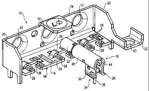
The preferred embodiment of multiple plug-in connector
lo for printed circuit boards according to the invention which
is shown in Figs. 1 to 3, for fastening to a printed
circuit board (not shown), comprises a mounting part 10
which has three openings 12, a first wall 14 which has a
printed-circuit-board side 16 adjacent the printed circuit
15 board, and a second wall 18 in which the openings 12 are
formed. The mounting part 10 also has side-pieces 20 which
are arranged perpendicularly to the first wall 14 and the
second wall 18. There is formed on one side-piece 20 a
fastening portion 22 which has an opening 23 for connecting
20 the mounting part 10 mechanically to the printed circuit
board, by means of a screwed connection for example. On a
contact-section side 24 of the first wall 14 which is
opposite from the printed-circuit-board side 16 are formed
first contact devices in the form of lugs 26 which rise up
25 in an arched shape. Formed on the printed-circuit-board
side 16 of the first wall 14 are second contact devices in
the form of contact areas 28 which project towards the
printed circuit board. When the mounting part 10 is fitted
onto the printed circuit board, these contact areas 28 come
30 to rest on corresponding contact pads on the printed
circuit board and are connected to the said contact pads
electrically by means of a soldered connection. The
mounting part is so designed that all the contact areas 28
CA 02740942 2011-04-13
WO 2010/060511 8 PCT/EP2009/007651
are within one common plane to within a tolerance of less
than 100 pm. It is ensured in this way that all the contact
areas 28 will make uniform contact with the contact pads on
the printed circuit board. The mounting part 10, and the
contact area 28 and lugs 26 which rise in an arched shape,
all of which are formed on the mounting part 10 in one
piece therewith, are entirely formed from an electrically
conductive material, and there is thus an electrically
conductive connection between all the lugs 26 which rise in
an arched shape and all the contact areas 28.
The multiple plug-in connector for printed circuit
boards which is shown by way of example also comprises
three contact sections 30, of which only one is shown for
reasons of clarity. The contact sections 30 take the form
of RF plug-in connectors each having a plug-in part 32 for
connecting by plugging-in to a complementary mating part
(not shown) of a plug-in connector (not shown). Each plug-
in part 32 is designed to engage in one of the openings 12,
as shown in Fig. 2. The contact sections 30 are pressed
into openings 12 by their respective plug-in parts 32.
Each contact section 30 also has a side 34 adjacent
the printed circuit board on which are arranged contact
members 36, 38. In the embodiment which is shown by way of
example, a first contact member 36 takes the form of an
outer-conductor contact and a second contact member 38
takes the form of a centre-conductor contact. The centre-
conductor contact 38 takes the form of a pin which extends
towards the printed circuit board beyond the first wall 14
of the mounting part 10 and which, when the mounting part
10 has been fitted down onto the printed circuit board,
engages in a corresponding mounting opening in the printed
circuit board and is electrically connected there to a
signal conductor on the printed circuit board, by soldering
CA 02740942 2011-04-13
WO 2010/060511 9 PCT/EP2009/007651
for example. This centre-conductor contact 38 is
electrically connected to a centre-conductor part 42 (Fig.
3) of the contact section 30, this centre-conductor part
extending into the plug-in part 32 and being held inside an
outer-conductor part 40 of the contact section 30 by means
of an insulator 44 (Figs. 1 and 2). The outer-conductor
contact 36 is electrically connected to the outer-conductor
part 40 and is designed to fit under the arched lugs 26. As
can be seen from Fig. 2, the outer-conductor contacts 36 of
lo the contact section 30 can be slid under the free ends of
the arched lugs 26, thus causing clamped electrical contact
to be made between the outer-conductor contacts 36 of the
contact section 30 and the arched lugs 26. An electrically
conductive connection between the outer-conductor contacts
36 of the contact section 30 and the contact areas 28 on
the first wall 14 of the mounting part 10 is thus made at
the same time via the electrically conductive mounting part
10.
The first wall 14 is made of an electrically
conductive material and the arched lugs 26 are thus
electrically connected to the contact areas 28. In this
way, the first wall 14 makes, via the arched lugs 26 and
the contact areas 28, electrical contact between the outer-
conductor contacts 36 and corresponding earth conductors on
the printed circuit board, with which earth conductors the
contact areas 28 make electrical contact. In other words,
this electrical contact by the outer-conductor contacts 36
of the contact sections 30 no longer has to be made
directly on the side 34 of the contact sections which is
adjacent the printed circuit board and instead it is the
mounting part 10 which takes over the making of this
electrical contact. This does away with the need for those
sides 34 of adjoining contact sections 30 which are
CA 02740942 2011-04-13
WO 2010/060511 10 PCT/EP2009/007651
adjacent the printed circuit board to be aligned in a plane
to an accuracy of 0.1 mm.
The mounting part 10 takes the form of a one-piece
stamped/punched and bent part having a finish of tin. This
allows the contact areas 28 to be soldered well to
corresponding contact pads on the printed circuit board.
The contact section 30, or rather the outer-conductor part
40 and the centre-conductor part 42, on the other hand are
preferably formed to have a finish of nickel, thus
resulting at the plug-in part 32 in good electrical contact
with the complementary mating connector with low insertion
forces. Because what occurs at the points of electrical and
mechanical contact between the outer-conductor contact 36
and the lugs 26 which rise in an arch is clamped contact
and not soldered contact, the nickel finish on the contact
section 30, which is difficult to solder, is not a
disadvantage.
This multiple plug-in connector for printed circuit
boards, or printed circuit board connector, according to
the invention thus separates the connecting interface at
the plug-in part 32 functionally from the soldered
electrical connection of the outer conductor 40 to
corresponding earth conductors on the printed circuit
board. This makes it possible for different coatings to be
used for the connecting interface at the plug-in part 32 on
the one hand and the soldered electrical connection of the
outer conductor 40 to corresponding earth conductors on the
printed circuit board on the other hand. The multiple plug-
in connector for printed circuit boards according to the
invention can be fitted out in a variety of ways, i.e. the
three contact sections 30 need not necessarily be of
identical forms. The system is particularly suitable for
single, double, treble and quadruple PCB connectors. Stand-
CA 02740942 2011-04-13
WO 2010/060511 11 PCT/EP2009/007651
off planarity for the outer-conductor contacts can easily
be obtained to within 0.1 mm even in multiple plug-in
connectors because the electrical contacts in question are
made by the contact areas 28 of the mounting part 10 and
s not directly by the outer-conductor contacts 36 on that
side 34 of the contact sections 30 which is adjacent the
printed circuit board.
The fact of contact being made with the earth
conductors on the printed circuit board by means of the
contact areas 28 of the mounting part 10 produces locally
defined points of electrical contact giving correspondingly
defined paths for the flow of current regardless of the
tin-lead solder, which may spread in unpredictable ways
during the soldering process. This latter would occur if
the printed-circuit-board side 16 of the first wall 14 were
to form a completely flat surface resting on the printed
circuit board.
The mounting part 10 has, on the side-pieces 20, at
least one pin 46 (four are shown in the illustrative
embodiment) which projects towards the printed circuit
board, to engage in a corresponding mounting opening in the
printed circuit board and to make a mechanical and/or
electrical connection to the printed circuit board.