Note: Descriptions are shown in the official language in which they were submitted.
CA 02740994 2011-04-18
WO 2010/023272 PCT/EP2009/061126
INLAYS FOR SECURITY DOCUMENTS
TECHNICAL FIELD
The invention relates to "inlay substrates" used in the production of "inlays"
for "security
documents" such as electronic passports and electronic identification cards.
BACKGROUND
A "security document" such as an electronic passport (ePassport) or an
electronic
identification (ell)) card may comprise an "inlay substrate" (or "inlay
laminate") which is
typically a sheet (or layer) of material such as TeslinTM, with a Radio
Frequency Identification
(RFID) chip module and corresponding antenna mounted therein. An ePassport may
have an
additional "cover layer" (or "cover material"), such as PVC-coated paper,
cloth or synthetic
leather laminated (or joined) thereto. An elD card may have an additional
upper "overlay
layer" of anti-scratch, typically transparent material, with an adhesive
backing laminated
thereto, and an additional "bottom layer", which may have a magnetic stripe.
In the main hereinafter, the inlay substrate (or inlay laminate) portion of
security documents
which are electronic passports (ePassport) are discussed. The inlay substrate,
with
transponder module and antenna incorporated therein may be referred to as a
"secure inlay".
Examples of Some Secure Documents
An electronic passport cover (or "e-cover") generally comprises a hinged cover
comprising a
front panel (or portion) and a back panel (or portion), and an insert of
several pages disposed
within the e-cover. The "passport card" is an alternative to an ordinary US
passport cover.
Both the passport cover and passport card include a vicinity-read radio
frequency
identification (RFID) chip. The RFID chip in the passport card (ell) card) is
designed to be
readable at a greater distance than that of the passport cover, and to prevent
the RFID chip
from being read when the passport card (ell) card) is not being used, the
passport card (ell)
card) typically comes with a sleeve designed to block the RFID chip from being
read while
the card is in the sleeve. See, for example, US Published Application No.
2007/0205953,
incorporated by reference herein.
FIG. IA shows an example of a security document which may an electronic
"passport cover"
(e-cover) comprising an inlay substrate (layer) and a cover layer (cover
material). An RFID
1
CA 02740994 2011-04-18
WO 2010/023272 PCT/EP2009/061126
chip module (not shown) and corresponding antenna (not shown) may be mounted
(disposed,
embedded) in the inlay substrate. An insert having several pages (not shown)
for presenting
printed information and receiving visa (entry and exit) stamps may be mounted
within the
passport cover. Notice that the passport cover, cover layer and inlay
substrate may be folded,
resulting in a front cover panel (portion) and a back cover panel (portion) of
the passport
cover. The passport cover is shown partially open (partially closed). In use,
when being
examined, scanned or stamped by a border (Vama, Duoanes) official, the
passport cover may
be fully open. When the passport cover is closed, the cover layer is external
to (surrounds)
the inlay substrate. The passport cover, cover layer and inlay substrate are
not shown to scale.
FIG. 1B shows an example of a security document which may be an identification
(eID) card
having an inlay substrate (layer), and additional layers comprising a top
overlay layer and a
bottom layer. An RFID chip module and corresponding antenna (not shown) may be
mounted
in the inlay substrate (middle layer). The additional top and bottom layers
may be anti-
scratch layers, and protect the inlay substrate in the middle from top and
bottom. The elD
card, inlay substrate layer and top and bottom layers are not shown to scale.
Examples of Some RFID Chip Modules
In the main hereinafter, the discussion may focus on RFID chip modules which
are leadframe-
type modules. However, some of the techniques for producing security documents
discussed
herein may also be applicable to epoxy glass modules (chip on FR4, wire
bonded, glob
topped).
FIG. 1C shows an example of an RFID chip module which is a "leadframe module"
comprising:
- a leadframe having a thickness of approximately 80 gm
- an RFID chip disposed on and connected by wire bonds to the leadframe,
having a
thickness of approximately 80 gm
- a mold mass disposed over the chip and wire bonds, having a thickness of
approximately 240 gm
- an antenna wire having end portions connected to "connection areas" of the
leadframe, typically on a side of the leadframe opposite the RFID chip (as
shown),
but the end portions can also be connected to connection areas on the same
side of the
lead frame as the RFID chip.
2
CA 02740994 2011-04-18
WO 2010/023272 PCT/EP2009/061126
The total thickness of the leadframe module may be 320 gm, such as for an
inlay substrate
having a thickness of approximately 356 gm. Generally, the chip module will be
disposed in
a recess in the inlay substrate so as to be concealed therein.
FIG. 1D shows an example of an RFID chip module which is an "epoxy glass
module"
comprising:
- an interconnect substrate, such as FR4 (printed circuit board substrate
material), having a
thickness of approximately 100 gm (FR4 is 100 gm and the chip & glob top 160
gm =
overall 260 gm)
- an RFID chip, wire-bonded (alternatively flip-chip connected with solder
bumps and
underfiller, as illustrated) to the FR4 substrate, having a thickness of
approximately 100
gm
- a glob top epoxy disposed over the chip and connections, having a thickness
with chip of
approximately 160 gm
- an antenna wire having ends connected to "connection pads", typically on the
same side
of the FR4 substrate as the RFID chip, but can also be connected on the
opposite side of
the FR4 substrate as the chip.
The total thickness of the epoxy glass module may be 260 gm, such as for an
inlay substrate
having a thickness of approximately 365 gm. Generally, the chip module will be
disposed in
a recess in the inlay substrate so as to be concealed therein.
Generally speaking, epoxy glass modules are inherently somewhat more flexible
than
leadframe modules. This is a factor that may need to be taken into
consideration when
incorporating an RFID module into a secure document. And, whereas leadframe
modules are
typically rectangular, the mold part (glob top) of an epoxy glass module are
typically round.
It should be understood that, although FIG. 1D shows a flip chip connection
between the
RFID chip and the FR4 substrate, the chip can be wire-bonded to the substrate
(such as was
shown in FIG. 1C, for the leadframe-type module.)
Some Definitions and Terminology
3
CA 02740994 2011-04-18
WO 2010/023272 PCT/EP2009/061126
An "inlay" or "inlay laminate" may comprise an "inlay substrate" which is a
planar sheet of
plastic material, such as TeslinTM. A "chip module" disposed in a "recess" in
the inlay
substrate. An antenna wire is mounted to the inlay substrate, such as be
embedding
(countersinking) within or adhesively attaching (sticking, placing) to a
surface of the inlay
substrate.
A chip module may include an RFID (radio frequency identification) chip and
means such as
a leadframe or an epoxy-glass (FR4) substrate for facilitating interconnecting
the RFID chip
with an antenna. Some RFID chips have integrated antennas, and do not require
the means
for interconnecting with and antenna. As used herein "chip" and "chip module"
can
encompass many configurations of a silicon die or a packaged chip.
The antenna is typically in the form of a flat coil of wire having a number
(such as 4 or 5) of
turns and two end portions which are connected to corresponding contact pads
(contact areas,
terminals) of the chip module. The antenna may be a dipole antenna having two
wire
segments with two inner ends, or any other antenna configuration suitable for
connection to a
chip or chip module in an inlay. The wire may include any elongate means for
conveying or
radiating signals, such as metallic wire (such as gold, aluminum, copper,
silver), of any profile
(such as round or rectangular), either bare, coated or color coated, as well
as optical fibers.
The recess for receiving the chip module extends into the inlay substrate from
a "top" surface
thereof, and may be a "window" type recess extending completely through the
inlay substrate
to a "bottom" surface thereof, or the recess may be a "pocket" type recess
extending only
partially through the inlay substrate towards the bottom surface thereof.
The recess may have a "straight" profile - in other words, substantially
constant cross-
dimension through (or into) the inlay substrate. Or, the recess may have a
"stepped" profile,
including a larger cross-dimension at the top surface of the substrate than at
(or towards) the
bottom surface of the inlay substrate. The recess is generally sized and
shaped to
accommodate the size and shape of the chip module being disposed therein. The
term
"cavity" may be used interchangeably with "recess".
A secure document, such as an electronic passport (e-passport) comprises an
"inlay" (inlay
substrate, plus chip module, plus antenna) and a "cover" layer (or substrate).
The inlay plus
4
CA 02740994 2011-04-18
WO 2010/023272 PCT/EP2009/061126
cover constitute an "e-cover". The "inlay" may be fully functional, but rarely
would be used
on its own, without additional, protective layers (such as the cover layer)
laminated thereto.
The inlay substrate may comprise, for example, TeslinTM, PVC, Polycarbonate
(PC),
polyethylene (PE) PET (doped PE), PETE (derivative of PE), and the like.
The cover layer may comprise, for example, PVC, coated offset board, with or
without optical
bleacher or acrylic coated cotton, supplied in web form or in sheets.
E-covers may be manufactured several at a time, such as "3up", on an "inlay
sheet" which
may include several (a plurality of) distinct "transponder areas" (or
"transponder sites") on an
"oversize" inlay substrate, for forming a plurality of e-covers. Each
transponder site may
comprise a chip module and antenna mounted to the inlay substrate. The chip
module and
antenna may be referred to as a "transponder". A cover layer may be laminated
(joined)
thereto, then the individual e-covers may be separated from the inlay sheet.
An Inlay and Transponder of the Prior Art
FIGs. IE and IF illustrate an inlay sheet 100 having a plurality of
transponder areas (or
sites). A selected one of the transponder areas 102 is shown in detail. The
vertical and
horizontal dashed lines (in FIG. 1E) are intended to indicate that there may
be additional
transponder areas (and corresponding additional transponders) disposed to the
left and right
of, as well as above and below, the transponder area 102, on the inlay sheet
100. As best
viewed in FIG. IF, the inlay sheet 100 may be a multi-layer substrate 104
comprising one or
more upper (top) layers 104a and one or more lower (bottom) layers 104b.
A recess 106 may be formed in (completely through) the upper layer 104a so
that a
transponder chip 108 may be disposed in the recess 106, and supported by the
lower layer
104b. The transponder chip 108 is shown having two terminals 108a and 108b on
a top
surface thereof.
This inlay sheet 100 is representative of a credit card, using hot lamination
to bond the
material. The overall thickness of the inlay sheet (104a and 104b) is
approximately 450 gm.
- the thickness of a top overlay layer (not shown), approximately 50 m
- the thickness of the top layer(s) 104a, approximately 400 m
CA 02740994 2011-04-18
WO 2010/023272 PCT/EP2009/061126
- depth of the recess 106, same as thickness of the top layer(s) 104a
- thickness of the transponder chip 108, approximately 320 gm
- thickness of the bottom layer(s) 104b, approximately 240 gm
Generally, the recess 106 is sized and shaped to accurately position the
transponder chip 108,
having side dimensions only slightly larger than the transponder chip 108 to
allow the
transponder chip 108 to be located within the recess 106. For example,
- the transponder chip 108 may measure: 5.0 x 8.0 mm
- the recess 106 may measure: 5.1 x 8.1 mm
- the terminals 108a/b may measure: 5.0 x 1.45 mm
- the wire (discussed below) may have a diameter between 60 and 112 gm
One millimeter (mm) equals one thousand (1000) micrometers (gm, "micron").
In FIGs. lE and IF, the recess 106 may be illustrated with an exaggerated gap
between its
inside edges and the outside edges of the chip 108, for illustrative clarity.
In reality, the gap
may be only approximately 50 m - 100 gm (0.05mm - 0.1 mm).
In FIG. lE the terminals 108a and 108b are shown reduced in size (narrower in
width), for
illustrative clarity. (From the dimensions given above, it is apparent that
the terminals 108a
and 108b can extend substantially the full width of the transponder chip 108.)
It should be understood that the transponder chip 108 is generally snugly
received within the
recess 106, with dimensions suitable that the chip 108 does not move around
after being
located within the recess 106, in anticipation of the wire ends 110a, 1 IOb
being bonded to the
terminals 108a, 108b.
As best viewed in FIG. 1E, an antenna wire 110 is disposed on a top surface
(side) of the
substrate 104, and may be formed into a flat (generally planar) coil, having
two end portions
l l0a and l 10b.
As best viewed in FIG. IF, the antenna wire 110 is "mounted" to the substrate
104a, which
may comprise "embedding" (countersinking) the antenna wire into the surface of
the
substrate, or "adhesively placing" (adhesively sticking) the antenna wire on
the surface of the
substrate. The wire typically feeds out of a capillary 116 of an ultrasonic
wire guide tool (or
6
CA 02740994 2011-04-18
WO 2010/023272 PCT/EP2009/061126
"sonotrode", not shown). The capillary 116 is typically disposed perpendicular
to the surface
of the substrate 100. The capillary 116 is omitted from the view in FIG. 1E,
for illustrative
clarity.
The antenna wire 110 may be considered "heavy" wire (such as 60 gm) and
requires higher
bonding loads than those used for "fine" wire (such as 30 gm). Rectangular
section copper
ribbon (such as 60 x 30 gm) can be used in place of round wire.
The capillary 116 may be vibrated by an ultrasonic vibration mechanism (not
shown), so that
it vibrates in the vertical or longitudinal (z) direction, such as for
embedding the wire in the
surface of the substrate, or in a horizontal or transverse (y) direction, such
as for adhesively
placing the wire on the surface of the substrate. In FIG. IF, the wire 110 is
shown slightly
spaced (in drawing terminology, "exploded" away) from the substrate, rather
than having
been embedded (countersunk) in or adhesively placed (stuck to) on the surface
of the
substrate.
The antenna wire 110 may be mounted in the form of a flat coil, having two
ends portions
l lOa and l IOb. The ends portions l lOa and l IOb of the antenna coil wire
110 are shown
extending over (FIG. 1E) and may subsequently be connected, such as by thermo-
compression bonding (not shown), to the terminals 108a and 108b of the
transponder chip
108, respectively.
Examples of embedding a wire in a substrate, in the form of a flat coil, and a
tool for
performing the embedding (and a discussion of bonding), may be found in US
Patent No.
6,698,089 (refer, for example, to FIGs. 1, 2, 4, 5, 12 and 13 of the patent).
It is known that a
coated, self-bonding wire will stick to a synthetic (e.g., plastic) substrate
because when
vibrated sufficiently to soften (make sticky) the coating and the substrate.
In FIG. IF, the wire 110 is shown slightly spaced (in drawing terminology,
"exploded" away)
from the terminals 108a/b of the transponder chip 108, rather than having been
bonded
thereto, for illustrative clarity. In practice, this is generally the
situation - namely, the end
portions of the wires span (or bridge), the recess slightly above the
terminals to which they
will be bonded, in a subsequent step. Also illustrated in FIG. IF is a
"generic" bond head,
7
CA 02740994 2011-04-18
WO 2010/023272 PCT/EP2009/061126
poised to move down (see arrow) onto the wire l IOb to bond it to the terminal
108b. The
bond head 118 is omitted from the view in FIG. 1E, for illustrative clarity.
The interconnection process can be inner lead bonding (diamond tool), thermo-
compression
bonding (thermode), ultrasonic bonding, laser bonding, soldering, ColdHeat
soldering
(Athalite) or conductive gluing.
As best viewed in FIG. 1E, due to the layout of the antenna coils, the antenna
wire 110 needs
to cross over itself. This is illustrated in the dashed-line circled area "c".
In order to prevent
shorting (electrical contact between different portions of the antenna coil)
the antenna wire
should be an insulated wire, generally comprising a metallic core and an
insulation (typically
a polymer) coating. Also, the polymer coating facilitates the wire being
"adhesively placed"
on (stuck to) a plastic substrate layer (such as 104a). (In some cases, the
antenna wire does
not need to cross over itself. See, for example, FIG. 4 of US Patent No.
6,698,089).
In order to feed the wire conductor back and forth through the ultrasonic wire
guide tool, a
wire tension/push mechanism (not shown) can be used or by application of
compressed air it
is possible to regulate the forward and backward movement of the wire
conductor by
switching the air flow on and off which produces a condition similar to the
Venturi effect.
By way of example, the wire conductor can be self-bonding copper wire or
partially coated
self-bonding copper wire, enamel copper wire or partially coated enamel wire,
silver coated
copper wire, un-insulated wire, aluminum wire, doped copper wire or litz wire.
The inlay substrate 104a may comprise PVC, PC, PE, PET, PETE, TYVEK, TESLIN,
Paper
or Cotton/Noil.
A cover layer (not shown) can be disposed over the inlay substrate 104a for
the final product,
which may be an e-ID card. See. FIG. 1B.
The conventional method of embedding an insulated copper wire into a synthetic
substrate is
described in US patent 6,233,818 and US patent 6,698,089 in which an
ultrasonic converter is
bolted to a sonotrode having a capillary hole to allow the passage of wire
from the side of the
sonotrode to the tip. The ultrasonic converter coaxially induces vibrations
into the sonotrode,
8
CA 02740994 2011-04-18
WO 2010/023272 PCT/EP2009/061126
thus creating localized friction and heat against the wire emerging from the
tip of the
sonotrode with a synthetic substrate. The wire is embedded into the substrate
by inducing
vibrations into the sonotrode and applying pressure, while at the same time
moving the
complete assembly to route the wire into the substrate to create an antenna
with several turns.
Embedding wire into a synthetic substrate such as PVC with a soft texture and
low melting
point can be accomplished using the conventional technique, but countersinking
an antenna
wire into a TeslinTM substrate, requires the additional procedure after the
wire embedding
process of pre-pressing the TeslinTM inlay in a lamination press.
Mounting an antenna wire to an inlay substrate by "embedding" or "adhesively
attaching"
have been mentioned, and are suitable for producing inlay substrates of secure
documents,
such as electronic passports. However, some of the techniques for producing
electronic
passports discussed herein may also be applicable to inlay substrates wherein
the antenna
comprises traces on an etched PWB (printed wiring board) or printed antenna
(conductive
ink) substrates. See, for example, US Patent Nos. 6,379,779; 6,406,935;
7,000,845;
7,449,212; and US Patent Publication Nos. 20090066076 and 20090115185, all of
which are
incorporated by reference herein.
An Example of Forming an Electronic Passport Cover (e-cover)
The production of an electronic passport cover (such as shown FIG. IA) in may
involve the
adhesive attachment of an inlay substrate with a cover layer.
FIG. 1G is a plan view illustrating an "inlay", (or "passport inlay", or "e-
cover inlay") for
preparing three (3) "passport covers" (such as shown in FIG. IA). The cover
layer 104 is
shown partially, so as to reveal the underlying inlay substrate 108. FIG. 1H
is a cross-
sectional view through FIG. 1G.
FIGs. 1G and 1H illustrate an e-cover inlay 100 having a "front" portion and a
"back"
portion, and comprising:
a cover layer (cover material) 104, such as approximately 350 gm thick; and
an inlay substrate 108, such as approximately 356 gm thick (14 mils) TeslinTM
9
CA 02740994 2011-04-18
WO 2010/023272 PCT/EP2009/061126
The material for the cover layer 104 may be PVC coated offset board or acrylic
coated cotton,
embossed and thermo-resistant. In the case of the fabric material, the
backside coating can be
water-base coated (aqueous / non-solvent), synthetic coated or have no
coating. The front
side coating can have two base coatings and one top coating of acrylic. An
alternative to
acrylic coating is peroxylene-based coating (nitrocellulose). The fabric can
have a strong bias
(diagonal) in the weave (drill weave as opposed to linear weave) which gives
it high tensile
strength and restricts the elongation. The leather embossing grain can have
the resemblance of
the skin of a kid goat or sheep (skiver) and is applied using an embossing
cylinder drum at a
pressure of 60 tons at around 180 degrees Celsius ( C). Because of the front
and backside
coatings the fabric is not porous.
The material for the cover layer 104 may be a cloth product, with chemistry in
the coatings
and a leather-like appearance to the cloth, such as by Holliston Inc. (905
Holliston Mills
Road, Church Hill, TN 37642; www.holliston.com)
The material for the inlay substrate 108 may be TeslinTM, a waterproof
synthetic film, single-
layer, uncoated with a thickness of 356 microns.
The material for the inlay substrate 108 may be PVC, PC, PE, PET, PETE, TYVEK,
TESLIN,
Paper or Cotton/Noil. The inlay substrate can also have special markings such
as luminous
threads, water marks, microscopic filings and optical polymer memory for
additional security.
The inlay format is typically "3up" (for making three passport covers at
once), and is
generally planar and rectangular, having exemplary overall dimensions of
404.81mm x
182.56mm x 0.70mm (thick). Each one of the three covers (A), (B) and (C) are
generally
rectangular, having exemplary dimensions of (404.81mm / 3) = 134.94mm x
182.56mm, with
a thickness of 0.70mm. In FIG. 1G, "A", "B" and "C", each are a "transponder
site" for a
given passport cover (see FIG. IA).
The inlay substrate 108 is prepared with index slots, holes, windows for the 3
chip modules'
mold mass and hinge gaps for the passport covers, and is then cut into sheets.
The
approximate width of the TeslinTM substrate is 248mm, whilst the cover layer
is
approximately 216 mm with a TeslinTM margin of 14 mm one side and 18 mm on the
other
side (248 = 216 + 14 + 18).
CA 02740994 2011-04-18
WO 2010/023272 PCT/EP2009/061126
A hinge gap 106 may be cut or punched through the inlay substrate 108 and the
cover layer
104, separating the "front" portion from the "back" portion of the passport
cover(s).
An RFID chip module 110 and corresponding antenna wire 120 are disposed in the
inlay
substrate 108.
- the chip module 110 may be a leadframe-type chip module (compare FIG. 1C)
comprising a chip encapsulated by a mold mass 112 and a leadframe 118.
- the mold mass may be approximately 240 gm thick and 5 mm wide
- the leadframe 118 may be approximately 80 gm thick and 8mm wide.
- the chip module 110 may have an overall size of 5.1 x 8.1 mm, encapsulation
size: 4.8 x
5.1 mm, leadframe thickness: 75 to 80 gm and overall thickness of the module
(leadframe and mold mass) approximately 320 gm.
- the antenna wire 120 may comprise 4 or 5 turns of wire, such as
approximately 80 gm
diameter (thick) wire. Ends of the antenna wire 120 are connected to the
leadframe 118,
such as described with respect to FIG. 1C.
The inlay substrate 108 may be prepared by embedding an insulated wire (such
as 80 m) into
the inlay substrate 108 to form an antenna 120 with 4 turns and
interconnecting the wire ends
of the antenna to a leadframe chip module by means of thermo-compression
bonding.
The leadframe chip module 110 may include a mold mass, such as epoxy or resin,
surrounding a silicon die on the leadframe 118. (see FIG. 1C)
The chip module 110 is disposed in a recess 116 in the inlay substrate. The
recess 116 may
be slightly wider than the module (compare FIG. 1F). The recess 116 may be a
"stepped"
recess, as shown, and may be a "window" recess extending completely through
the inlay
substrate 108. Normally, the opening of the recess 116 at the bottom of the
inlay substrate
108 is left open, revealing the mold mass 112 (flush with the bottom surface),
which presents
security problems.
The recess 116 has a larger cross-dimension at the top surface of the inlay
substrate 108 to
accept the protruding leadframe 112 on each side of the chip module, and this
larger portion
11
CA 02740994 2011-04-18
WO 2010/023272 PCT/EP2009/061126
of the recess may be formed by using an ultrasonic stamp to create a dent
(depression) into the
top surface of the inlay substrate 108.
A stepped recess, such as the recess 116 shown in FIG. 1H may be created in a
single layer
by first forming a window opening through the layer, then compressing the
layer (such as the
inlay substrate 108) to form a "shoulder" (region of reduced cross-dimension)
around a
periphery of the window opening. See US 2009/0091424, incorporated by
reference herein.
The cover layer 104 is laminated (joined) to the inlay substrate 104 using a
polyurethane hot
melt adhesive 114, such as approximately 50-80 m thick. Prior to the adhesive
process, the
inlay substrate may be pre-pressed to ensure that the antenna wire does not
protrude over
(extend above) the surface of the TeslinTM substrate, in other words, to
ensure that the antenna
wire is fully embedded in the inlay substrate.
Non-reactive adhesives based on polyamide are typically not used in electronic
passports for
security reasons, as it would be possible to de-laminate the material by
applying heat.
Instead, reactive adhesive, moisture curing hot melt adhesive based on
polyurethane, is used.
Many are available.
The adhesive can be characterized by a high initial tack and a long open time
(several
minutes) or a short setting time (several seconds). In the latter case, the
adhesive has to be
reactivated using infra red light before the cover layer is attached to the
inlay, or hot
laminated within a certain period (within 1 to 2 hours). The adhesive cures
exclusively in the
presence of moisture and gains its final strength after 3 to 7 days.
The adhesive may be applied to the cover layer (cover material) at
approximately 150 degrees
Celsius, putting down a layer of 50 to 80 microns ( m). The inlay is applied
to the cover
layer (cover material) in web or in sheet form, and is then laminated together
using a roll
press. Thereafter, the laminated inlay with the cover layer (cover material)
is cut to size and
stored in a stack for 3 to 7 days in a storage area having a regulated
temperature and humidity.
Some Technical (Physical) Problems Associated With Using Hot-Melt Adhesive
The technique of applying moisture-curing hot melt based on polyurethane to a
cover material
processed in web form may have a number of drawbacks:
12
CA 02740994 2011-04-18
WO 2010/023272 PCT/EP2009/061126
The back side of the cover material has a non-smooth (grained) texture which
prevents a
homogenous layer of adhesive coating being applied, irrespective of the
coating applicator
such as slot nozzle, screen printing, spray applicator or flexo/gravure
roller. In the event of
over-coating in a humid environment, leaving an uneven thickness of adhesive
on the cover
layer, the probability of C02 emission after lamination is quite high. The
release of C02 gas
from the adhesive layer results in the formation of bubbles between the cover
material and
the Teslin inlay.
The tensile strength properties and the thermal expansion coefficient of the
cover material
differ significantly from that of TeslinTM. During the coating process in
which adhesive is
applied to the cover material at approximately 150 Celsius and thereafter
during the roll
press lamination process to reactivate the adhesive at 125 Celsius, the
TeslinTM inlay held at
room temperature is positioned onto the cover material, meaning that the
different thermal
expansion of the substrates can lead to sideways displacement of the finished
product. This
mechanical displacement results in the so-called "banana effect" in which the
electronic
passport cover is curve shaped (warped).
As the cover layer (cover material) in web form is stretched across drums
during the coating
and lamination processes, the cover layer (cover material) memorizes the
curved shape of the
drums which can present a problem during curing. If the final product is
stored in stacks
under the pressure of a weight, separated by paper sheets, in a non-controlled
temperature and
humidity environment, the optimal curing time of 3 to 7 days will vary
significantly according
to production batches. The resulting effect of a short curing time is the
warping of the final
product.
Apart from the formation of bubbles and the warping of the final product, the
longevity of the
electronic passport could be reduced by moisture seeping into the exposed area
around the
mold mass of the chip module.
Some Security Concerns Regarding Secure Documents
Apart from the above "technical" issues (physical problems) which impinge on
the quality,
reliability and longevity of secure documents, there may be a number of
additional concerns
13
CA 02740994 2011-04-18
WO 2010/023272 PCT/EP2009/061126
surrounding (i) security and (ii) the type of chip module (such as leadframe
module, or epoxy
glass module) used, for example, in a passport inlay.
To prevent or indicate tampering of the area surrounding the chip module, it
is advantageous
to hide the transponder chip or chip module and the wire interconnections
thereto in the inlay
substrate layer to enhance protection against falsification. Security elements
may also be
designed in particular as optically variable elements, such as holograms,
electroluminescent
pigments, or interference layer elements for example which, when viewed, give
different
color impressions depending on the viewing angle.
One of the impediments in hiding the transponder chip module and the wire
interconnections
thereto in the inlay substrate layer (thickness: 356 microns) has been the
thickness of the chip
module with 320 microns. In addition, metal leadframe chip modules mounted to
an inlay
substrate tend to break during torsion and bending of the substrate.
Semiconductor
companies have reduced the footprint and thickness of the chip module down to
250 microns,
by packaging the transponder chips as a flip-chip module, glass epoxy module,
plastic
leadframe module or as naked die connected directly to the wire ends of an
antenna.
To prevent external skimming of the data stored in the transponder chip when a
passport is
closed, it is desired that an electromagnetic shield be integrated into the
front and back cover
of a passport cover. See, for example, US 2007/0205953 (Axalto), incorporated
in its
entirety by reference herein.
Glossary & Definitions
Unless otherwise noted, or as may be evident from the context of their usage,
any terms,
abbreviations, acronyms or scientific symbols and notations used herein are to
be given their
ordinary meaning in the technical discipline to which the disclosure most
nearly pertains. The
following terms, abbreviations and acronyms may be used throughout the
descriptions
presented herein and should generally be given the following meaning unless
contradicted or
elaborated upon by other descriptions set forth herein. Some of the terms set
forth below may
be registered trademarks ( ).
Chip As used herein, the word "chip" can encompass many configurations of a
silicon die or a packaged chip. The silicon die for example can have
metallized
14
CA 02740994 2011-04-18
WO 2010/023272 PCT/EP2009/061126
bumps to facilitate the direct connection of the wire ends of an antenna to
form
a transponder or tag device. A package chip can include various structures
such
as a tape automated bonding module, a chip module, a flip chip module, a
leadframe, a glass epoxy flexible module, a chip carrier, a strap, an
interposer
or any form of packaging to facilitate transponder manufacturing.
Electronic It is a proprietary material that is processed into a film for
integration into
Ink electronic displays. The principal components of electronic ink are
millions of
tiny microcapsules. Each microcapsule contains positively charged white
particles and negatively charged black particles suspended in a clear fluid.
When a negative electric field is applied, the white particles move to the top
of
the microcapsule where they become visible to the user. This makes the
surface appear white at that spot. At the same time, an opposite electric
field
pulls the black particles to the bottom of the microcapsules where they are
hidden. By reversing this process, the black particles appear at the top of
the
capsule, which now makes the surface appear dark at that spot. To form an E
Ink electronic display, the ink is printed onto a sheet of plastic film that
is
laminated to a layer of circuitry. The circuitry forms a pattern of pixels
that can
then be controlled by a display driver. These microcapsules are suspended in a
liquid "carrier medium" allowing them to be printed using existing screen
printing processes onto virtually any surface, including glass, plastic,
fabric
and even paper.
Faraday Faraday shield is an enclosure formed by conducting material, or by a
mesh
Cage of such material. Such an enclosure blocks out external static electrical
fields.
Faraday cages are named after the English scientist Michael Faraday, who
invented them in 1836. A Faraday cage's operation depends on the fact that
an external static electrical field will cause the electrical charges within
the
cage's conducting material to redistribute themselves so as to cancel the
field's
effects in the cage's interior. This phenomenon is used, for example, to
protect
electronic equipment from lightning strikes and other electrostatic
discharges.
To a large degree, Faraday cages also shield the interior from external
electromagnetic radiation if the conductor is thick enough and any holes are
significantly smaller than the radiation's wavelength.
CA 02740994 2011-04-18
WO 2010/023272 PCT/EP2009/061126
FR-4 FR-4, an abbreviation for Flame Retardant 4, is a type of material used
for
making a printed circuit board (PCB). It describes the board substrate, with
no
copper layer. FR-4 meets the requirements of Underwriters Laboratories
UL94-V0. The FR-4 used in PCBs is typically UV stabilized with a
tetrafunctional epoxy resin system. It is typically a transparent yellowish
color
- the green, red and sometimes blue color of a finished board comes from the
solder mask. FR-4 manufactured strictly as an insulator (without copper
cladding) is typically a difunctional epoxy resin system and a greenish color.
FR-4 is similar to an older material called G-10. G-10 lacked FR-4's self-
extinguishing flammability-characteristics. FR-4 has widely replaced G-10 in
most applications. Some military applications where destruction of the circuit
board is a desirable trait will still utilize G-10.
Inlay An inlay substrate typically has a plurality, such as array of
transponder sites
on a substrate which matches the position of the data or graphics on a printed
sheet or holder / cover page of a smart card or electronic passport
respectively.
A secure inlay is similar to a conventional inlay but with additional features
such as an additional RFID chip on the transponder site storing information
about the production processes in the value chain as well as having
personalization features integrated into the inlay such as a hologram, an anti-
skimming material or security codes embedded into the inlay.
Laminating As used herein, in its most general sense, laminating refers to
joining two (or
more) sheets of material to one another. The sheets may be the same material
as one another. Two different (and distinct) kinds of lamination are discussed
herein.
Hot Lamination which used temperature and pressure to cause the two
sheets of material to fuse with one another
Cold Lamination in which an adhesive is used to join the two sheets of
material to one another.
Laser Laser ablation is the process of removing material from a solid (or
occasionally
16
CA 02740994 2011-04-18
WO 2010/023272 PCT/EP2009/061126
Ablation liquid) surface by irradiating it with a laser beam. At low laser
flux, the
material is heated by the absorbed laser energy and evaporates or sublimates.
At high laser flux, the material is typically converted to a plasma. Usually,
laser ablation refers to removing material with a pulsed laser, but it is
possible
to ablate material with a continuous wave laser beam if the laser intensity is
high enough.
The depth over which the laser energy is absorbed, and thus the amount of
material removed by a single laser pulse, depends on the material's optical
properties and the laser wavelength. Laser pulses can vary over a very wide
range of duration (milliseconds to femtoseconds) and fluxes, and can be
precisely controlled. This makes laser ablation very valuable for both
research
and industrial applications.
The simplest application of laser ablation is to remove material from a solid
surface in a controlled fashion. Laser machining and particularly laser
drilling
are examples; pulsed lasers can drill extremely small, deep holes through very
hard materials. Very short laser pulses remove material so quickly that the
surrounding material absorbs very little heat, so laser drilling can be done
on
delicate or heat-sensitive materials.
A typical laser for ablating synthetic material such as TeslinTM or
Polycarbonate is an ultra violet diode pump laser operating at the wavelength
of 385nm.
Metallic Metallic pigments such as aluminium pigments are utilized in the
coating
Pigments industry to fulfil functional requirements such as electrical
conductivity and
shielding in consumer electronics. Typical metal pigments range from
approximately 3 m (offset printing) to over 50 m.
Mold Mold mass is the part of a chip module which encapsulates the area
Mass surrounding a silicon die mounted on a leadframe or carrier and the wire
bond
connections (Au wire 0 24 m) thereto. The mold mass is typically epoxy
duraplast and the encapsulation process is transfer molding. Alternatively,
the
17
CA 02740994 2011-04-18
WO 2010/023272 PCT/EP2009/061126
silicon die and wire interconnections can be protected by dispensing a fast
curing resin (glob top).
Patch A piece of material used to cover a hole, cavity or recess area in a
substrate layer
assigned to a transponder chip and or antenna, used to protect and
hermetically
seal the underlying chip and interconnections thereto, to prevent moisture
seeping into and electro-static discharge (ESD) entering the assigned area,
having security elements which may overlap onto the substrate layer. The patch
may be attached to the substrate layer by means of adhesion, lamination under
pressure and temperature, laser welding, ultrasonic collation, etc.
Printed Printed Silicon Electronics refers to semiconductor technology using
printable
Silicon silicon-based inks, additive printing techniques and thin film
technology.
Electronics Silicon ink, oxide inks and metal inks are deposited on thin metal-
foil
substrates. After the ink is printed, it forms silicon islands that are
annealed to
drive out the solvents, leaving a polysilicon crystal film. Oxide inks are
used
to create a gate dielectric, other inks for in situ n- and p-type dopants and
metal inks for contacts to the silicon.
Reactive In general, one-component moisture-curing polyurethane hot-melt
adhesive-
Adhesive based on reaction products from di- or polyisocyanates and polyether-
polyols,
crystalline or partly crystalline polyester-polyols and low molecular weight
polymers from olefinically unsaturated monomers and optionally
hydroxylated tackifying resins.
RFID Short for "Radio Frequency Identification". An RFID device interacts,
typically
at a limited distance, with a "reader", and may be either "passive" (powered
by
the reader) or "active" (having its own power source, such as a battery).
Teslin A single layer of microporous, polyolefin-based, uncoated film that
bonds
readily and firmly with toners, inks, adhesives and laminating films. Teslin
is a
waterproof synthetic material that works well with an inkjet printer, laser
printer,
or thermal printer. Teslin is also single-layer, uncoated film, and extremely
strong. In fact, the strength of the lamination peel of a Teslin sheet is 2-4
times
18
CA 02740994 2011-04-18
WO 2010/023272 PCT/EP2009/061126
stronger than other coated synthetic and coated papers. Teslin comes in the
sizes
of 7 mil to 18 mil, though only sizes 10 mil and 14 mil are sized at 8.5" by
11",
for printing with most consumer printers. Also available are perforated
versions
of Teslin, specifically, lup, 2up, 3up, 6up, and Sup. Teslin is used widely in
the production of drivers licenses, voter ID cards, and other forms of
identification card. Because of its commercial availability, Teslin is also
often
found used for counterfeit or fake IDs. "Teslin" is a registered trademark of
PPG Industries, Inc. for synthetic printing sheet.
SUMMARY OF THE INVENTION
It is a general object of the invention to provide improved techniques for use
in the
manufacture of security documents, and security documents (the "product")
having improved
technical and security features. For example,
- improvements in the manufacture of the product to reduce warpage and
breakage in the
product, and to integrate and hide the chip module and the wire
interconnections in an
inlay substrate layer of the product and add security features to make
alteration of the
product and/or the production of forgeries technically impossible or at least
uneconomical.
- unauthorized separation of the cover material and inlay substrate
mechanically or through
de-lamination should result in the destruction of the chip module and the
antenna
- to prevent skimming of the personal data stored in the memory of an RFID
chip in an
electronic passport by activating the secure document with correct keys at
close proximity
or eavesdropping by intercepting the communication between a reader and an
electronic
passport, shielding is required.
Some features and embodiments disclosed herein may be concerned with
techniques to
protect a chip module from moisture and mechanical shock using a adhesive
patch; to hide an
antenna in a multi-layered construction; to create recesses in a substrate to
accommodate a
chip module leadframe using laser ablation instead of compressing the material
to form a
recess; to loop the wire ends of an antenna adjacent to the terminals areas of
a chip module in
preparation for interconnection, and to embed a wire conductor into a
substrate using a wire
guide assembly consisting of an ultrasonic converter, aluminum block directing
the ultrasonic
energy and a sonotrode.
19
CA 02740994 2011-04-18
WO 2010/023272 PCT/EP2009/061126
Other features disclosed herein may be concerned with security issues: to hide
a chip (die,
leadframe chip module, epoxy glass chip carrier, etc) in a substrate using
stepped recesses to
accommodate the chip and a patch or patches to protect the chip and the wire
interconnections
thereto; to integrate security features into the inlay such as a hologram,
metal security strip or
an electronic ink display which can be activated by the electro-magnetic field
driving the
RFID chip,-and to shield a transponder unit in a passport cover from
authorized skimming
when the passport cover is closed, by adding metallic pigments to the adhesive
layer bonding
the cover layer to the inlay substrate.
According to an embodiment of the invention, an inlay substrate for a secure
document
having a recess extending into the inlay substrate from a first (top) surface
thereof for
receiving a chip module therein, and an antenna wire disposed in the inlay
substrate and
connected with the chip module, the inlay substrate comprises: at least two
layers of a
synthetic material, such as TeslinTM, laminated to one another with a layer of
adhesive. The
chip module may be a leadframe-type module or an epoxy glass type module.
The antenna wire may be disposed on a top one of the at least two layers, or
between the at
least two layers.
The recess may be straight or stepped. The recess may be a pocket-type recess
extending only
partially through the substrate or a window-type recess extending completely
through the
inlay substrate. The recess may be formed by laser ablation, or by freezing
the material of the
inlay substrate and machining (milling) it.
A moisture-resistant patch may cover the chip module. An epoxy filling may be
disposed in
the recess, surrounding the chip module and the antenna wire interconnections.
A lid may
covering an opening of the recess.
Channels may be formed (pre-formed) in a surface of the substrate within which
the antenna
wire is at least partially embedded. The channels may be formed by removing
material or
displacing material. The channels may be formed by at least one of (i) laser
ablation, (ii)
gouging, (iii) ultrasonic stamp, and (iv) heating and molding.
CA 02740994 2011-04-18
WO 2010/023272 PCT/EP2009/061126
The channels define a pattern for the antenna. An antenna wire may be mounted
in the
channel.
Rather than using antenna wire, the channels may be filled with a flowable,
conductive
material to form the antenna. Techniques are disclosed for connecting the
flowable,
conductive material with terminals of a chip module.
Ferrite material may be incorporated into the inlay substrate to reflect or
absorb
electromagnetic energy. Various embodiments are disclosed.
A cover layer may be laminated to the inlay substrate. The cover layer and
inlay substrate
may comprise an inlay, such as for a passport booklet (cover) having a front
panel and a back
panel. A shielding / detuning antenna may be disposed on the back panel of the
passport
cover. A switch may be disposed in the passport cover for disconnecting the
chip module's
antenna when the passport booklet is closed.
BRIEF DESCRIPTION OF THE DRAWINGS
Reference will be made in detail to embodiments of the disclosure, examples of
which may be
illustrated in the accompanying drawing figures (FIGs). The figures are
intended to be
illustrative, not limiting. Although the invention is generally described in
the context of these
embodiments, it should be understood that it is not intended to limit the
invention to these
particular embodiments.
Certain elements in selected ones of the figures may be illustrated not-to-
scale, for illustrative
clarity. The cross-sectional views, if any, presented herein may be in the
form of "slices", or
"near-sighted" cross-sectional views, omitting certain background lines which
would
otherwise be visible in a true cross-sectional view, for illustrative clarity.
In some cases,
hidden lines may be drawn as dashed lines (this is conventional), but in other
cases they may
be drawn as solid lines.
If shading or cross-hatching is used, it is intended to be of use in
distinguishing one element
from another (such as a cross-hatched element from a neighboring un-shaded
element). It
should be understood that it is not intended to limit the disclosure due to
shading or cross-
hatching in the drawing figures.
21
CA 02740994 2011-04-18
WO 2010/023272 PCT/EP2009/061126
Elements of the figures may (or may not) be numbered as follows. The most
significant digits
(hundreds) of the reference number correspond to the figure number. For
example, elements
of Figure 1 are typically numbered in the range of 100-199, and elements of
FIG. 2 are
typically numbered in the range of 200-299. Similar elements throughout the
figures may be
referred to by similar reference numerals. For example, the element 199 in
FIG. 1 may be
similar (and possibly identical) to the element 299 in FIG. 2. Throughout the
figures, each of
a plurality of elements 199 may be referred to individually as 199a, 199b,
199c, etc. Such
relationships, if any, between similar elements in the same or different
figures will become
apparent throughout the specification, including, if applicable, in the claims
and abstract.
FIG. IA is a perspective view of a security document which is a passport cover
(e-cover),
according to the prior art.
FIG. 1B is a perspective view of a security document which is an electronic
identification
card (ell)), according to the prior art.
FIG. 1C is a perspective view of a chip module which is a leadframe module,
according to
the prior art.
FIG. 1D is a perspective view of a chip module which is an epoxy-glass module,
according to
the prior art.
FIG. lE is a top view of a transponder site (one of many on an inlay sheet),
according to the
prior art.
FIG. IF is a side, cross-sectional view, partially exploded, of a wire being
mounted to the an
inlay substrate and bonded to the terminals of a transponder chip, according
to the prior art.
FIG. 1G is a top view of an inlay sheet for making e-covers, having three
"transponder sites"
("3up"), according to the prior art.
FIG. 1H is a side, cross-sectional view, partially exploded, of an e-cover of
FIG. 1G.
22
CA 02740994 2011-04-18
WO 2010/023272 PCT/EP2009/061126
FIG. 2A is a cross-sectional view, illustrating a passport cover comprising a
multi-layer inlay
substrate and a patch covering a chip module in a recess of the inlay
substrate, according to an
embodiment of the invention.
FIG. 2B is a cross-sectional view, illustrating a passport cover comprising a
multi-layer inlay
substrate and a patch covering a chip module in a recess of the inlay
substrate, according to an
embodiment of the invention.
FIGs. 2C, 2D and 2E are cross-sectional views showing a method of making the
passport
cover in FIG. 2B, according to an embodiment of the invention.
FIG. 2F is a cross-sectional view, illustrating a passport cover comprising a
multi-layer inlay
substrate and a patch covering a chip module in a recess of the inlay
substrate, according to an
embodiment of the invention.
FIG. 2G is a cross-sectional view, illustrating a passport cover comprising a
multi-layer inlay
substrate and a patch covering a chip module in a recess of the inlay
substrate, according to an
embodiment of the invention.
FIG. 2H is a cross-sectional view, illustrating a passport cover comprising a
multi-layer inlay
substrate and a chip module in a pocket-type recess of the inlay substrate,
according to an
embodiment of the invention.
FIG. 21 is a cross-sectional view, illustrating a passport cover comprising a
multi-layer inlay
substrate and a chip module in a pocket-type recess of the inlay substrate,
according to an
embodiment of the invention.
FIG. 2J is a cross-sectional view, illustrating a passport cover comprising a
single layer inlay
substrate and a chip module in a pocket-type recess of the inlay substrate,
according to an
embodiment of the invention.
FIG. 3A is a perspective view illustrating a technique for forming a recess in
an inlay
substrate using laser ablation, according to an embodiment of the invention.
23
CA 02740994 2011-04-18
WO 2010/023272 PCT/EP2009/061126
FIG. 3B is a cross-sectional view illustrating a technique for forming a
recess in an inlay
substrate using laser ablation, according to an embodiment of the invention.
FIG. 3C is a cross-sectional view illustrating a technique for forming a
recess in an inlay
substrate using laser ablation, according to an embodiment of the invention.
FIG. 3D is a cross-sectional view illustrating a technique for forming a
recess in an inlay
substrate using laser ablation, according to an embodiment of the invention.
FIG. 4A is a cross-sectional view illustrating a technique for creating
channels for mounting
an antenna wire in an inlay substrate, according to an embodiment of the
invention.
FIG. 4B is a cross-sectional view illustrating a technique for creating
channels for mounting
an antenna wire in an inlay substrate, according to an embodiment of the
invention.
FIG. 4C is a cross-sectional view illustrating a technique for creating
channels for mounting
an antenna wire in an inlay substrate, according to an embodiment of the
invention.
FIG. 4D is a perspective view illustrating a technique for creating channels
for mounting an
antenna wire in an inlay substrate, according to an embodiment of the
invention.
FIG. 4E is a cross-sectional view illustrating mounting an antenna wire in a
channel,
according to an embodiment of the invention.
FIG. 4F is a cross-sectional view illustrating an antenna wire mounted in a
channel,
according to an embodiment of the invention.
FIG. 4G is a cross-sectional view illustrating mounting an antenna wire in a
channel,
according to an embodiment of the invention.
FIG. 4H is a cross-sectional view illustrating an antenna wire mounted in a
channel,
according to an embodiment of the invention.
24
CA 02740994 2011-04-18
WO 2010/023272 PCT/EP2009/061126
FIG. 41 is a cross-sectional view illustrating a flowable, conductive material
being applied on
a surface of a substrate to fill a channel, according to an embodiment of the
invention.
FIG. 4J is a cross-sectional view illustrating a further step in the technique
of applying a
flowable, conductive material on a surface of a substrate to fill a channel,
according to an
embodiment of the invention.
FIG. 4K is a cross-sectional view illustrating a flowable, conductive material
being applied to
fill a channel in a layer of adhesive, according to an embodiment of the
invention.
FIG. 4L is a cross-sectional view illustrating a further step in the technique
of applying a
flowable, conductive material to an adhesive layer to fill a channel,
according to an
embodiment of the invention.
FIG. 4M is a top of an inlay substrate with recess for a leadframe-type chip
module and
channels for a flowable, conductive material, according to an embodiment of
the invention.
FIG. 4N is a cross-sectional view illustrating a flowable, conductive material
in channels
formed in a surface of a substrate, and connecting the conductive material to
terminals of a
chip module, according to an embodiment of the invention.
FIG. 4P is a cross-sectional view illustrating a further step in the technique
of connecting a
flowable, conductive material in channels formed in a surface of a substrate
with terminals of
a chip module, according to an embodiment of the invention.
FIG. 4Q is a cross-sectional view of a technique for connecting a flowable,
conductive
material in channels formed in a surface of a substrate with terminals of a
chip module,
according to an embodiment of the invention.
FIG. 5A is a top of an inlay substrate with recess for a leadframe-type chip
module and
channels for antenna wire, according to an embodiment of the invention.
CA 02740994 2011-04-18
WO 2010/023272 PCT/EP2009/061126
FIG. 5B is a side, cross-sectional view of the inlay substrate of FIG.SB,
showing embedding
an antenna wire in the channel, and bonding end portions of the antenna wire
to terminals of
the chip module, according to an embodiment of the invention.
FIG. 5C is a top of an inlay substrate with recess for an epoxy glass type
chip module and
channels for antenna wire, according to an embodiment of the invention.
FIG. 5D is a side, cross-sectional view of the inlay substrate of FIG.SC,
showing embedding
an antenna wire in the channel, and bonding end portions of the antenna wire
to terminals of
the chip module, according to an embodiment of the invention.
FIG. 6A is a cross-sectional view, illustrating an inlay substrate with a
pocket-type recess,
and a patch (lid) covering an opening of the recess, according to an
embodiment of the
invention.
FIG. 6B is a cross-sectional view, illustrating an inlay substrate with a
window-type recess,
and patches (lids) covering openings in the top and bottom of the recess,
according to an
embodiment of the invention.
FIG. 7A is a top view of a security feature which may be used in an embodiment
of the
invention.
FIG. 7B is a top view of a the security feature of FIG. 7A.
FIG. 7C is a perspective view of a security feature which may be used in an
embodiment of
the invention.
FIG. 7D is a cross-sectional view of a security feature which may be used in
an embodiment
of the invention.
FIG. 7E is a top view of a security feature which may be used in an embodiment
of the
invention.
26
CA 02740994 2011-04-18
WO 2010/023272 PCT/EP2009/061126
FIG. 7F is a diagrammatic cross-sectional view of a security feature which may
be used in an
embodiment of the invention.
FIG. 8A is a cross-sectional view of a coated wire which may be used with
embodiments of
the invention.
FIG. 8B is a cross-sectional view of a using a laser to remove insulation from
a coated wire, a
feature which may be used with embodiments of the invention.
FIG. 8C is a cross-sectional view of a security feature which may be used with
embodiments
of the invention.
FIG. 8D is a cross-sectional view showing a technique for direct connection of
the antenna
wire to an RFID chip, according to an embodiment of the invention.
FIG. 8E is a perspective view related to the technique for direct connection,
according to an
embodiment of the invention.
FIG. 8F is a plan view of a feature of an embodiment of the invention.
FIG. 9A is a cross-sectional view showing an embodiment of incorporating
ferrite material
into the inlay substrate, according to an embodiment of the invention.
FIG. 9B is a cross-sectional view showing an embodiment of incorporating
ferrite material
into the inlay substrate, according to an embodiment of the invention.
FIG. 9C is a cross-sectional view showing an embodiment of incorporating
ferrite material
into the inlay substrate, according to an embodiment of the invention.
FIG. 9D is a cross-sectional view showing an embodiment of incorporating
ferrite material
into the inlay substrate, according to an embodiment of the invention.
FIG. 9E is a cross-sectional view showing an embodiment of incorporating
ferrite material
into the inlay substrate, according to an embodiment of the invention.
27
CA 02740994 2011-04-18
WO 2010/023272 PCT/EP2009/061126
FIG. 10A is a side view of a sonotrode of the prior art (such as in US Patent
6,698,089).
FIG. lOB is a cross-sectional view of an ultrasonic wire guide (embedding)
tool, according to
an embodiment of the invention.
FIG. 1OC is a perspective view of the ultrasonic wire guide tool shown in FIG.
9B.
DETAILED DESCRIPTION
Various "embodiments" of the invention (or inventions) will be discussed. An
embodiment
is an example or implementation of one or more aspects of the invention(s).
Although various
features of the invention(s) may be described in the context of a single
embodiment, the
features may also be provided separately or in any suitable combination.
Conversely,
although the invention(s) may be described herein in the context of separate
embodiments for
clarity, the invention(s) may also be implemented in a single embodiment.
The relationship(s) between different elements in the figures may be referred
to by how they
appear and are placed in the drawings, such as "top", "bottom", "left",
"right", "above",
"below", and the like. It should be understood that the phraseology and
terminology
employed herein is not to be construed as limiting, and is for descriptive
purposes only.
The invention relates generally to inlays and techniques for making the
inlays, including
technical features and security features. As used herein, an "inlay" may be a
single- or multi-
layer substrate containing HF (high frequency) and/or UHF (ultra-high
frequency) radio
frequency identification (RFID, transponder) chips and/or modules. These
inlays may be
used in secure documents, such as, but not limited to, electronic passports
(ePassports) and
electronic ID (ell)) cards.
Some Embodiments of the Invention
Various embodiments of the invention will be presented to illustrate the
teachings of the
invention(s). In the main, examples of electronic passport covers with inlay
substrates having
leadframe modules may be used to illustrate the embodiments. It should be
understood that
various embodiments of the invention(s) may also be applicable to other secure
documents
containing electronics (such as RFID and antenna), such as electronic ID
cards. Secure
28
CA 02740994 2011-04-18
WO 2010/023272 PCT/EP2009/061126
documents may also be referred to as "electronic documents". In the main
hereinafter, secure
documents which are passport inlays, typically cold laminated (with adhesive),
are discussed.
The following embodiments and aspects thereof may be described and illustrated
in
conjunction with systems, tools and methods which are meant to be exemplary
and
illustrative, not limiting in scope. Specific configurations and details may
be set forth in order
to provide an understanding of the invention. However, it should be apparent
to one skilled in
the art that the invention(s) may be practiced without some of the specific
details being
presented herein. Furthermore, well-known features may be omitted or
simplified in order not
to obscure the descriptions of the invention(s).
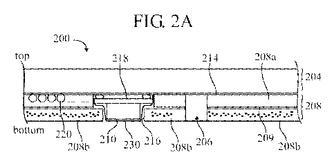
A Multi-Layer Inlay Substrate, and a Patch (FIGs. 2A, 2B)
FIGs. 2A and 2B illustrate embodiments of a secure document which is an inlay
200 suitable
for use as a passport cover. The inlay 200 comprises a multiple-layer inlay
substrate 208 and
a cover layer 204 cold laminated (adhesively attached, joined) to the inlay
substrate 208 with
a layer 214 of adhesive such as 50 gm, which may be applied by roller coater.
A hinge gap 206 is shown in FIG. 2A (and in other figures). The hinge gap 206
may simply
be a gap, approximately 1 mm wide, between a left (as viewed) portion of the
inlay substrate
208 and a right (as viewed) portion of the inlay substrate 208. The left
portion of the inlay
200 corresponds to the front of the passport cover (FIG. IA), and the right
portion of the inlay
200 corresponds to the back portion of the passport cover (FIG. IA).
Notice that, in FIG. 1G, the hinge gaps 106 do not completely separate the
back portion of
the inlay substrate from the front portion, they are still joined by a "web".
Typically, the gap
is punched or cut after adhesive coating and pre-press lamination (to smooth
the surface)
The cover layer 204 is generally a planar sheet or layer of flexible, durable,
often "textile-
type" material, such as PVC, coated offset board, with or without optical
bleacher or acrylic
coated cotton.
The inlay substrate 208 (both layers 208a and 208b) is generally a planar
layer or sheet of
flexible, durable, typically "plastic-type" material, such as TeslinTM, PVC,
Polycarbonate
29
CA 02740994 2011-04-18
WO 2010/023272 PCT/EP2009/061126
(PC), polyethylene (PE) PET (doped PE), PETE (derivative of PE), and the like.
The
material of the inlay substrate may be referred to as "synthetic paper".
The inlay substrate, or a bottom layer thereof (particularly when the antenna
is embedded on a
top surface of the top layer), can also be conductive, such as a ferrite-
coated or ferrite-
containing substrate to reflect or absorb electromagnetic energy. This is
indicated by the
particles (dots) in the bottom inlay substrate layer 208b of FIG. 2A.
FIG. 9A (compare FIG. 2A) illustrates a multi-layer inlay substrate 908
(compare 208). The
inlay substrate 908 comprises an upper layer 908a (compare 208a) laminated
with an adhesive
909 (compare 209) to a lower layer 908b (compare 208b). A cover layer 904
(compare 204)
may be laminated with an adhesive 914 (compare 214) to the inlay substrate
908.
A ferrite layer (dots) can be created in a synthetic substrate layer 908b
beneath the layer 908a
in which the antenna wire 920 (or conductive material forming an antenna) is
located, being
applicable to all types of antennae such as wire embedded, etched or
conductive ink antennae.
FIG. 9B illustrates that the inlay substrate layer 908a in which the antenna
wire 920 is
embedded may be a ferrite-coated synthetic layer (having a ferrite coating
908c). Since the
antenna wire 920 is embedded in the ferrite-containing material, a coated
(insulated) antenna
wire, such as shown in FIG. 8A should be used. See, for example, Flexield
Series Flexible
Composite-Type Electromagnetic Shield Materials For 13.56MHz RFID System, TDK
Corporation, Tokyo Japan, incorporated by reference herein. See also US Patent
No.
4,539,433, incorporated by reference herein. For a multi-layer inlay
substrate, this could be
the top layer (208a).
FIG. 9C illustrates that a recess (or cavity) may be created by mechanically
milling or laser
ablating a layer of the inlay substrate, then filling the recess with ferrite
material (metal or
nano-metal particles) and conductive polymers, to create a 3D ferrite-
structured layer. Here,
the lower layer 908b is provided with the recess 925 which is filled with
ferrite particles. The
recess 925 may extend completely through the layer 908b, or only partially
through the layer
908b. After the ferrite filling is cured, the area may be sealed with a patch
(not shown) of
synthetic material.
CA 02740994 2011-04-18
WO 2010/023272 PCT/EP2009/061126
The ferrite material can be applied using digital non-impact inkjet printing,
conventional
printing (flexography, gravure, screen printing, offset) or dispensing. The
area of the ferrite
layer is larger than the area occupied by the antenna, in order to ensure
optimal reflection of
the electromagnetic energy.
FIG. 9D illustrates that the recess to accommodate the ferrite material can
also be produced
by using multiple layers with a cavity or cavities in the center substrate
layer or layers. Only
the bottom layer 908b is shown, for illustrative clarity.
Here, the bottom layer 908b comprises a sandwich construction of a top layer
927a, a middle
layer 927b and a bottom layer 927c. The middle layer 927b has a window-type
recess 927
extending completely therethrough, and filled with ferrite material.
FIG. 9E (compare FIG. 9C) illustrates that the ferrite material may be
disposed in a recess
929, such as in the top layer 908a, and after the ferrite filling is cured,
the area may be sealed
with a patch 930 of synthetic material. The antenna wire 220 can also be
embedded into the
same layer as the ferrite material and routed across the sealed patch 930 to
form the antenna
pattern.
Returning to FIGs. 2A and 2B, an antenna wire 220 is mounted to a top surface
of the inlay
substrate 208, and a chip module 210 is disposed in a recess 216 extending
into the inlay
substrate 208 from a top surface thereof. The antenna wire 220 may comprise 4
or 5 turns of
wire, such as approximately 80 gm diameter (thick) wire. Ends of the antenna
wire 220 are
connected to terminals of the chip module 210.
The recess 216 may be a window-type recess extending completely through the
inlay
substrate 208 to the bottom surface thereof. of the inlay substrate.
The chip module 210 may be a leadframe-type chip module comprising a chip
mounted on a
leadframe 218 and encapsulated by a mold mass 212. The leadframe 218 may be
approximately 80 gm thick and 8 mm wide. The mold mass 212 may be
approximately 240
gm thick and 5 mm wide. The chip module 210 may have an overall size (width
dimensions)
of 5.1 x 8.1 mm and an overall thickness of 320 gm. The width of the recess
216 should be
sufficient to accommodate the chip module (including leadframe 218), with some
clearance.
31
CA 02740994 2011-04-18
WO 2010/023272 PCT/EP2009/061126
The inlay substrate 208 comprises two or more layers 208a and 208b which are
laminated
(adhesively attached, joined) one another with a layer (or layers) 209 of
adhesive such as 50-
80 m, which may be applied by a roller coater. In the main hereinafter, a two-
layer example
of an inlay substrate 208 will be described, comprising an upper (topmost)
layer 208a and a
lower (bottommost) layer 208b.
The recess 216 for the chip module 210 extends into the inlay substrate 208
from the top
surface of the topmost layer 208a, through the topmost layer 208a, and at
least partially into
the bottommost layer 208b. The recess 216 extends fully through the entire
inlay substrate
208, including fully through the bottommost layer 208a, exiting the inlay
substrate 208 at the
bottom of the bottommost layer 208b.
The recess 216 is "stepped" in that it has a larger width dimension opening at
the top surface
of the inlay substrate 208 than at the bottom surface of the inlay substrate
208. For example,
a top portion of the recess 216, for accommodating the leadframe 218 has a
width dimension
of 5.3 x 8.1 mm, and a bottom portion of the recess 216 for accommodating the
mold mass
212 has a width dimension of 5.1 x 5.1 mm.
The stepped recess 216 may be formed by a first opening having a first width
dimension in
the topmost layer 208a, second opening having a second width dimension in the
next adjacent
(which is the bottommost) layer 208b. When the layers 208a and 208b are
assembled with
one another, the openings in the layers 208a and 208b are aligned (such as
concentric) with
one another. The first width dimension is different than the second width
dimension. The
first width dimension, for accommodating the leadframe, is shown greater than
the second
width dimension, for accommodating the mold mass.
The openings of the recess 216 in the layers 208a and 208b may be any
appropriate shape,
such as rectangular for a rectangular chip module or circular for a circular
(round) chip
module. The openings may be formed by a mechanical punch operation.
In the prior art (FIG. 1H), a stepped recess may be formed in a single layer
inlay substrate
108. by compressing the substrate using an ultrasonic stamp. An advantage of
forming the
32
CA 02740994 2011-04-18
WO 2010/023272 PCT/EP2009/061126
inlay substrate 208 with (at least) two layers 208a and 208b is that the
stepped recess may be
formed more easily, and precisely.
The chip module 110 disposed in the recess 216 in such a way that the
leadframe 218 is
nearly flush with the upper surface of the top substrate layer 208a and the
mold mass of the
chip module is nearly flush with a bottom side of the bottom substrate layer
208b. However,
note that the end portions of the antenna wire 220 are connected (bonded) to
the top surface of
the leadframe 218 (opposite the chip and mold mass which are on the bottom
surface of the
leadframe 218. Also note that the diameter of the antenna wire 220 is
decreased where it is
bonded to the leadframe 218. For example, the 80 m wire may be compressed to
approximately 40 m during thermo-compression bonding.
In the finished inlay substrate 208, which may be considered an "interim
product", all of the
components (chip module 210 and antenna 220) mounted in or to the inlay
substrate 208
should not project beyond the surface of the inlay substrate 208.
In FIG. 2A, the antenna wire 220 is embedded (disposed) in a top surface of
the topmost
substrate layer 208a, and is connected with a top surface of the leadframe
218.
In FIG. 2B, the antenna wire is embedded between the two adjacent inlay
substrate layers
208a and 208b, such as in a top surface of the bottom substrate layer 208b, or
in the bottom
surface of the top substrate layer 208a.
FIG. 2B differs from FIG. 2A in that the antenna wire (which may be self-
bonding wire) is
disposed between the two substrate layers 208a and 208b (rather than atop the
top layer 208a).
This may be accomplished by:
- first, with the top layer 208a inverted (bottom side up), partially
embedding the antenna
wire 220 into the bottom surface of the top layer 208a, without countersinking
the
antenna wire 220 entirely, leaving the antenna wire 220 to protrude above the
layer. For
example, the antenna wire 220 is embedded only approximately 30-70% of its
diameter
into the bottom surface of the top layer 208a, leaving 70-30% protruding above
the
bottom surface of the top layer 208a. Or, the antenna wire 220 is embedded
only
approximately 40% or 50% of its diameter into the bottom surface of the top
layer 208a
33
CA 02740994 2011-04-18
WO 2010/023272 PCT/EP2009/061126
leaving 60% or 50%, respectively, protruding above the bottom surface of the
top layer
208a. See FIG. 2C.
- then, in a second step, the top layer 208a is flipped over (top side up),
and is adhesively
attached to the bottom layer 208b carrying the antenna, whereby the protruding
antenna
wire 220 is positioned face down onto the top surface of the bottom layer
208b, before
lamination. In the lamination process, the antenna wire 220 sinks into the
bottom layer
208b. The lamination process has also the advantage of "disguising" the
position of the
antenna in the two layered inlay substrate structure and creating a smooth and
even
surface on each external surface (top surface of the top layer, bottom surface
of the
bottom layer) of the multi-layered inlay substrate structure. See FIGs. 2D and
2E.
- Another feature of FIG. 2B is the wire ends of the antenna are connected to
the face-
down side of the chip module leadframe.
- An advantage of this inlay construction is that any attempt to peel the two
layers apart,
results in the destruction of the antenna and the wire interconnections to the
chip module.
The chip module may be mounted face- down into the first layer 208a, then the
antenna 208
is scribed into the opposite side of the first layer 208a, and the wire ends
are connected to the
chip module 210.
During the lamination process, the adhesive 209 compresses, some squeezes out,
and some
may get absorbed into the cover layer during the lamination process. After
lamination, the
adhesive layer 209 may be only 20 m thick. The layers 208a and 208b may be
"pre-
pressed" with a hot laminator to smooth the surface and hide the wires.
During embedding of the antenna wire, the wires "mark" the inlay substrate.
The material
may be flattened by putting the inlay substrates through temperature and
pressure for about 30
minutes.
A security feature of the antenna wire location (between the two layers) shown
in FIG. 2B is
that if an attempt is made to pull the chip module out of the inlay, this may
destroy the
interconnections and wire antenna.
It should be understood that there are various "combinations" of module
orientation and
interconnection location which may be shown in FIGs. 2A & 2B, 2F & 2G, 2H, 21
& 2J, 5B,
34
CA 02740994 2011-04-18
WO 2010/023272 PCT/EP2009/061126
5G, 6A & 6B. Generally, the module can be mounted face down or face up and the
interconnections thereto can be on the top of the module such as is the case
with a leadframe
or underneath the chip carrier (epoxy glass or leadframe).
FIGs. 2C, 2D and 2E show a method of making the inlay substrate 208 of FIG.
2B.
- (FIG. 2C) with the top layer 208a inverted (or, invert the top layer 208a),
so the bottom
surface is facing up, partially embed the antenna wire 220 in the upward-
facing bottom
surface of the top layer 208a, leaving a portion of the (diameter of) the
antenna wire
protruding from the surface;
- (FIG. 2D) flip over (un-invert) the top layer 208a so that its bottom
surface is facing
downwards (and top surface is facing upwards).
- (FIG. 2E) laminate (with adhesive) the top layer 208a (which has the antenna
wire
protruding from the surface) to the bottom layer 208b, thereby embedding the
protruding
portion of the antenna wire 220 into the top surface of the bottom layer 208b.
Alternatively, the antenna wire 220 can first be partially embedded in the top
surface of the
bottom layer 208b, then in the lamination process, sunk into the bottom
surface of the top
layer 208a.
Alternatively, the antenna wire 220 can be positioned between two adjacent
layers of the inlay
substrate, then partially embedded into both layers, adhesively bonded and
then laminated to
form one cohesive electronic laminate layer. Any attempt to separate the two
layers may
result in the destruction of the antenna and the wire-end connections to the
chip module.
Some additional exemplary dimensions for the inlay 200 are:
- overall thickness of the inlay 200, approximately 700 gm (0.700mm),
including cover
layer 204 and adhesive layers 214 and 209
- thickness of the cover layer 204, approximately 300 gm
- thickness of the inlay substrate 208, approximately 356 m
- thickness of each layer 208a and 208b of the inlay substrate 208,
approximately 145 gm
- thickness of the adhesive 209 joining the two inlay substrate layers 208a
and 208b,
approximately 50 gm
- thickness of the adhesive 214 joining the cover layer 204 to the topmost
layer 208 of the
inlay substrate 208, approximately 50 gm
CA 02740994 2011-04-18
WO 2010/023272 PCT/EP2009/061126
FIG. 2B also illustrates a "deep trench" formed extending from the bottom
surface of the top
layer, to within the top layer 208a, for routing the antenna wire 220 to the
chip module 510.
The formation of "channels" and "deep trenches" is discussed in greater detail
hereinbelow,
such as with respect to FIGs. 4A and 5D
An additional feature shown in FIGs. 2A and 2B is a patch 230 covering
(overlying) the chip
module 210 and connections with the antenna wire 220. For example, the patch
230 may be
made of the same material as the substrate (such as TeslinTM) - laminated,
adhesively attaches,
ultrasonic or laser welding - 50 gm thick. This patch 230 is not exclusive to
the inlay
substrate 208, rather it could be used, for example, with the inlay substrate
108 of FIG. 1H.
In situations where the recess 216 extends completely through the inlay
substrate 208, the
patch 230 may seal the area of the chip module 210 from moisture. The patch
230 may be
moisture-resistant.
The patch 230 can be antistatic, to protect the chip module from electrostatic
discharge.
The patch 230 may comprise a material that is luminous under ultraviolet (UV)
light, so that
tampering with the patch can be exposed by presenting the inlay 208 to an
ultraviolet light
source. As is known,
To help thwart counterfeiters, sensitive documents (e.g. credit cards,
driver's licenses,
passports) may also include a UV watermark that can only be seen when viewed
under
a UV-emitting light. Passports issued by most countries usually contain UV
sensitive
inks and security threads. Visa stamps and stickers on passports of visitors
contain large
and detailed seals invisible to the naked eye under normal lights, but
strongly visible
under UV illumination. Passports issued by many nations have UV sensitive
watermarks on all pages of the passport. Currencies of various countries'
banknotes
have an image, as well as many multicolored fibers, that are visible only
under
ultraviolet (UV) light.
FIGs. 2F and 2G illustrate embodiments of a secure document which is an inlay
200 suitable
for use as a passport cover. A cover layer 204 is laminated with adhesive 214
to a multi-layer
inlay substrate 208 comprising at least two layers 208a and 208b' (prime),
laminated with an
36
CA 02740994 2011-04-18
WO 2010/023272 PCT/EP2009/061126
adhesive 209 to one another. A chip module 210 comprising a chip (not shown),
a leadframe
218 and a mold mass 212 is disposed in a recess 216 extending into the inlay
substrate 208
from a top surface thereof, and the recess 216 is stepped.
FIG. 2F illustrates an embodiment of a secure document which is an inlay 200
suitable for
use as a passport cover. This inlay is substantially the same as the inlay 200
shown in FIG.
2A (multi-layer inlay substrate 208, antenna wire 220 on top of top inlay
substrate layer
208a), with the addition of a strip (or stripe) 232 of a material, such as
metal or Mylar, having
a thickness of approximately 10 gm applied around the area where the patch 230
and the inlay
substrate 208 (the bottom of the bottom inlay layer 208b) meet, bridging any
gap between the
bottom of the patch 230 and the bottom of the inlay substrate 208. The stripe
232 crosses any
void between the patch 230 and the bottom surface of the inlay substrate 208.
FIG. 2G illustrates an embodiment of a secure document which is an inlay 200
suitable for
use as a passport cover. This inlay is substantially the same as the inlay 200
shown in FIG.
2B (multi-layer inlay substrate 208, antenna wire 220 between the two
substrate layers 208a
and 208b). However, rather than using a patch (230), an epoxy filling 234,
which may be
luminescent under UV light, may be disposed in the recess, surrounding the
chip module and
the antenna wire interconnections. This may provide evidence of tampering when
exposed to
an ultraviolet light source.
FIGs. 2H and 21 show "variations" of inlays shown in FIGs. 2A and 2B. In most
respects,
the inlays 200' (prime) of FIGs. 2E and 2F are similar to the inlays 200 of
FIGs. 2A and 2B.
A cover layer 204 is laminated with adhesive 214 to a multi-layer inlay
substrate 208
comprising at least two layers 208a and 208b' (prime), laminated with an
adhesive 209 to one
another. A chip module 210 comprising a chip (not shown), a leadframe 218 and
a mold mass
212 is disposed in a recess 216 extending into the inlay substrate 208 from a
top surface
thereof, and the recess 216 is stepped.
In FIG. 2H, in a manner similar to that shown in FIG. 2A, the antenna wire 220
extends
along (within) the top surface of the top layer 208a, and connects to the top
surface of the
leadframe 218.
37
CA 02740994 2011-04-18
WO 2010/023272 PCT/EP2009/061126
In FIG. 21, in a manner similar to that shown in FIG. 2B, the antenna wire 220
is disposed
between the top layer 208a and the bottom layer 208b, and connects to the
bottom surface of
the leadframe 218.
A feature shown in the embodiments of FIGs. 2H and 21 (and 2J), is that rather
than the
recess 216 being a "window-type" recess extending completely through the inlay
substrate
208' (prime), the recess 216' (prime) is a "pocket-type" recess extending only
partially through
the inlay substrate 208'. In the embodiments of FIGs. 2H and 21, the recess
216' stops short
of the bottom surface of the bottom layer 208b', leaving (for example)
approximately 10 gm
of material 208c directly under the chip module 210. This essentially
eliminates the need for
the patch 230 (FIGs. 2A, 2B), since there is no opening at the bottom surface
of the inlay
substrate 208' caused by the recess 216'.
At "first glance" it may appear that the multi-layer inlay substrate 208 is
not significantly
different than the "one or more" top layers 104a of the inlay sheet 100 shown
in FIG. IF.
However, there are a number of significant differences, such as:
- the layers of a credit card (including, if applicable, multiple layers of
the inlay substrate)
are hot laminated to one another
- the layers of the passport booklet, such as the cover layer and the inlay
layer (including,
if applicable, multiple layers of the inlay substrate) are cold laminated to
one another,
with adhesives.
- the credit card is much thicker, making it easier to conceal and protect the
RFID chip
- the antenna wire is embedded in a different plane
- the layers of the inlay substrate 208 are adhesively attached to one
another, attempts to
separate the two layers is intended to result in the destruction of the chip
module and the
antenna. This is an important security feature.
- The standard construction of a multi-layered inlay (such as suggested by the
"one or
more" top layers 104a) is to hot laminate the substrate together. There is no
adhesive
layer (209). This is generally not possible with a synthetic paper material
like TeslinTM.
- I E and 1 F are standard contactless card. 1 F, if complete would have
another layer on
top 0.78mm. (For ID cards, this is important, as they all follow the ISO 7816
standard
for dimensions.)
- in a passport, the material of cover layer is different than material of
inlay substrate
38
CA 02740994 2011-04-18
WO 2010/023272 PCT/EP2009/061126
- in the contactless card (FIG. 1F) the cover layer (not shown) would be of
the same
material as the layer 104.
- The thickness of a credit card (FIG. 1F) is sufficient to cover and protect
the chip and
antenna. For example, 450 m
- With a passport (FIGs. 2A-21), the chip module is approximately as thick as
the inlay
substrate (both are in the range of 300 - 400 gm). It is more difficult to
protect the chip
module 210 in the passport than in the credit card. (A credit card 450 m
thick, and the
chip module is surrounded by the substrate layer. In the passport, the
substrate does not
cover the chip, entirely.)
In the embodiments described above, with respect to FIGs. 2A-21, the inlay
substrate layers
(such as TeslinTM) are adhesively attached to form the inlay substrate 208
integrating the
transponder (chip module 210) in the center of the inlay 200. Any attempt to
separate the two
layers (208a, 208b) should result in the destruction of the inlay 200. Also
the patch 230
protects the chip module 210.
FIG. 2J shows another variation on the inlay 200" (double prime). Again, most
of the
elements are the same as for the inlays 200 and 200', and the inlay 200" is
nearly identical to
the inlay 200'. A cover layer 204 is laminated to the inlay substrate 208, an
antenna 220 is
mounted to the inlay substrate 208, and a chip module 210 is disposed in a
stepped, pocket-
type recess 216'. However, here, the inlay substrate 208" (double prime) is
formed in a single
layer inlay substrate 208".
Fabricating the Inla.. (Passport Cover)
Various methods may be used to fabricate the passport cover (200) such as:
- The first and second layers (208a and 208b) of the inlay substrate (208) may
be
adhesively attached to one another in sheet (rather than roll) format.
- The cover material (204) may also be processed in sheet format by applying a
layer of
polyurethane hot melt adhesive with a short opening time using a roller
coating machine.
- The adhesive-coated cover material (204) may be positioned on the multi-
layered inlay
substrate and affixed at two (or more) points using an ultrasonic collator.
- The inlay substrate (208) may then be laminated to the cover material (204)
by
reactivating the polyurethane hot melt adhesive in a hot roll or lamination
press.
39
CA 02740994 2011-04-18
WO 2010/023272 PCT/EP2009/061126
- Instead of applying heat to the cover material, it can be advantageous to
apply the heat to
the inlay substrate at a temperature of approximately 120 Celsius by passing
the cover
and inlay substrate over a hot lamination roll, under a pressure of
approximately 3 Bar.
The layers of the multi-layer inlay substrate (208) and the cover layer (204)
may be handled
in sheet format and not from a web or an endless reel during the coating and
lamination
processes in which the material, held under tension, is passed over hot and
cold rollers. Web
coating and laminating over rollers is the primary cause of curling of the
finished product.
To avoid the so-called banana effect of curling inlays after adhesively
attaching the cover
layer to the inlay substrate, the reactive hot melt adhesive may be applied to
the cover layer in
sheet format. For security reasons, the peel strength of the laminated inlay
with the cover
layer should meet or exceed the ICAO standard (ISO/IEC 10373). This can be
achieved by
applying the correct thickness of adhesive during the coating stage, exerting
the correct
pressure and temperature during the reactivation stage and storing the
finished product to
complete the curing process in a moisture controlled environment.
An Alternative to Hot Melt Adhesive
In another embodiment of the invention, a solution is provided which minimizes
the emission
of C02 gas resulting in the formation of bubbles between a passport cover
layer and the
underlying inlay substrate. Instead of applying hot melt adhesive to the
structured cover layer
resulting in an uneven thickness of adhesive, a thin layer of aliphatic
adhesive (as opposed to
aromatic adhesive) high in viscosity (34,000 mPas at 130 Celsius) may be
applied with a
short open time of several seconds to the inlay substrate using a slot nozzle
system (with
shims). See, for example, Jowat 628.80.
In order to be able to apply the aliphatic adhesive under light pressure to
the inlay substrate, it
is advisable that the slot nozzle head does not go against the "grain" of the
protruding antenna
wires at the position of the chip module. For this reason, the slot nozzle
head applying the
adhesive may be applied in the direction of the wire ends, and not in the
direction of the
antenna.
CA 02740994 2011-04-18
WO 2010/023272 PCT/EP2009/061126
After applying the aliphatic adhesive, but before the aliphatic adhesive is
reactivated, the
hinge gaps may be punched in the inlay substrate. And, finally, the cover
layer may be placed
over the inlay substrate and laminated in a press to create the passport
cover.
Mechanically Milling the Recess
A problem with mechanical milling a synthetic material such as TeslinTM is
that it is a
flexible (resilient, deformable). It is no problem to punch out a hole through
a layer of
TeslinTM and, as described above, a stepped opening can be made by
compression.
According to a feature of the invention, a recess (stepped or straight) can be
formed in a
material such as TeslinTM used for the inlay substrate by mechanical milling,
by first reducing
the temperature of the TeslinTM to make it more rigid and machineable. For
example, below
-10 C, such as approximately -18 C. Refrigeration and cooling units are well
known. The
material may be removed from the refrigeration unit immediately prior to
machining (milling)
and/or may be maintained at a low temperature during machining, such as by
directing a
stream of cooled air at the workpiece.
Numerous recesses in inlay substrates are illustrated herein, and milling is
well known. A
suitable milling tool is available from IBAG Switzerland AG, operating at
30,000 to 60,000
RPM, moving at 1-4 meters per minute (mpm).
Forming Recesses in Inlay Substrates, using Laser Ablation
US Application No. 12/045,043 (Publication No. 2008/0179404) describes (see
FIG. 8 therein)
a technique for forming a recess in a substrate. As described therein ...
The laser 860 emits a beam (dashed line), targeted at the substrate 802, to
ablate
material from the substrate 802 to form the recess 806. The beam may have a
diameter
of approximately 0.1 mm. The beam may be scanned back and forth, traversing in
one
direction entirely across the recess area, turning around, and traversing back
across the
recess area, like plowing a field. Many passes may be required to carve out
the entire
area of the recess, given that the beam diameter is typically much (such as 10-
100
times) smaller than the length or width of the recess. As is known, the beam
may be
scanned, in any suitable manner, such as with mirrors. Also, the intensity of
the beam
may be controlled or modulated to control the penetration into the substrate.
For
41
CA 02740994 2011-04-18
WO 2010/023272 PCT/EP2009/061126
example, a pulse-width modulated beam may be used. The laser may be a UV laser
(355nm) with a power ranging from 20 to 70 watts.
The process of using a laser in this manner, rather than (for example) a
conventional
rotating milling tool, may be referred to as "laser milling". The technique
described
herein may be particularly beneficial for applications where it is desired to
form a
"pocket" type recess which intentionally does not extend all the way through
the
substrate or sheet (in other words, the recess or pocket extends only
partially through
the substrate). Mechanical milling can be difficult. On the other hand, laser
milling
can be very effective for Teslin and polycarbonate substrates. For PVC, laser
milling is
less effective.
In another embodiment of the invention use is made of a TeslinTM inlay
substrate to
accommodate a 3up format (182.56mm x 404.81mm) with a thickness of 356 m,
prepared
with milled cavities (laser abrasion or mechanically milled) with a depth of
95 m on each
side of an opening to accept a leadframe or glass epoxy chip module. Before a
chip module is
placed in each of the three pockets, as described, an ultra violet adhesive
with reflecting
particles is dispensed for the purpose of holding a chip module in placed as
well as a security
feature to indicate tampering. In the next step of the process, an insulated
self bonding wire
with a diameter of approximately 80 m is embedded into the TeslinTM inlay
substrate;
scribing an antenna with 4 turns; looping the wire ends of the antenna
adjacent to the terminal
areas of a chip module; removing the wire insulation before interconnection,
drawing the
looped wires on each side of the chip module over the terminal areas; and
bonding the wire
ends to the leadframe or glass epoxy tape by means of thermo compression
bonding. After
bonding, the wire ends are deformed to a thickness of approximately 40 m.
Given that the thickness of the chip module (leadframe: 80 m and mold mass
240 m) is
approximately 320 m and the inlay substrate 356 m, the connected antenna
wires to the
leadframe of the chip module may protrude over the inlay by approximately 40
m. The
antenna is embedding entirely into the inlay substrate using an ultrasonic
embedding head
assembly with booster, alternatively the antenna can be pressed into the
substrate using a
heated stamp the size of the antenna or laminated in a conventional press.
Typically the
lamination process results in the shrinkage of the inlay substrate, and
therefore it can be
42
CA 02740994 2011-04-18
WO 2010/023272 PCT/EP2009/061126
advantageous to punch the hinge gap (106, FIG. 1G) in the inlay substrate
after lamination to
remain in tolerance.
FIGs. 3A-3D illustrate various techniques for using a laser to ablate material
in a controlled
manner from a substrate such as an inlay substrate (such as 208) to form a
recess (such as
126) extending into a surface of the inlay substrate.
FIG. 3A shows forming a recess (opening, window) in a single layer of
material, such as a
layer of TeslinTM for an inlay substrate (compare 106, FIG. 1F), using laser
ablation. This
single layer of material may also be representative of each of the two layers
in a multi-layer
inlay substrate such as are shown in FIGs. 2A and 2B.
FIG. 3A illustrates an exemplary process 300 of forming a recess 316 in an
inlay substrate
308, using a laser 360. The inlay substrate 308 may be a single layer of
Teslin (for example),
having a thickness "t" of 355 gm. A typical size (width dimensions) for the
recess 316, to
accommodate a chip module (such as 210) with a lead frame (such as 218), may
be
approximately 5 mm x 8 mm. The recess 316 may extend completely through the
inlay
substrate 308, resulting in a window-type recess. The recess 316 may extend
only partially,
such as 260 gm through the inlay substrate 308, resulting in a pocket-type
recess.
The laser 360 emits a beam (dashed line), targeted at the substrate 302, to
ablate material from
the substrate 308 to form the recess 316. The beam may have a diameter of
approximately 0.1
mm. The beam may be scanned back and forth, traversing in one direction
entirely across the
recess area, turning around, and traversing back across the recess area, like
plowing a field.
Many passes may be required to carve out the entire area of the recess, given
that the beam
diameter is typically much (such as 10 - 100 times) smaller than the length or
width of the
recess. As is known, the beam may be scanned, in any suitable manner, such as
with mirrors.
Also, the intensity of the beam may be controlled or modulated to control the
penetration into
the substrate. For example, a pulse-width modulated beam may be used. The
laser may be a
UV laser (355 nm) with a power ranging from 20 to 70 watts.
The process of using a laser in this manner, rather than (for example) a
conventional rotating
milling tool, may be referred to as "laser milling". The technique described
herein may be
particularly beneficial for applications where it is desired to form a
"pocket" type recess
43
CA 02740994 2011-04-18
WO 2010/023272 PCT/EP2009/061126
which intentionally does not extend all the way through the substrate or sheet
(in other words,
the recess or pocket extends only partially through the substrate). Mechanical
milling can be
difficult. On the other hand, laser milling can be very effective for Teslin
and polycarbonate
substrates. For PVC, laser milling is less effective.
The recess (opening) 316 formed in the inlay substrate layer 308 of FIG. 3A
extends
completely through the inlay substrate layer 308. The layer may be
representative of each of
the at least two inlay substrate layers 308a and 308b shown in FIGs. 2A and 2B
which, to
form a stepped recess (216) would have two different-size openings formed
therein.
FIG. 3B shows forming a stepped window-type recess 316r in a single layer of
material, such
a layer of TeslinTM for an inlay substrate 308r (compare 108, FIG. 1H), using
laser ablation.
This may be a two-step process comprising:
- first laser milling a central area (such as between "b" and "c") to a first
partially through
the substrate,
- then continuing laser milling the entire area (such as between "a" and "c")
to create a
recess extending partially through the substrate in a peripheral area, and to
extend the
recess in the central area completely through the substrate.
Alternatively:
- first laser milling the entire area (between "a" and "d") to a first depth
(dl)
- then laser milling only the central area (between "b" and "c") to a second
depth (d2).
FIG. 3C shows forming a stepped pocket-type recess 316s in a single layer of
material, such a
layer of TeslinTM for an inlay substrate 308s (compare 108, FIG. 1H), using
laser ablation.
This may be a two-step process comprising:
- first laser milling a central area (such as between "b" and "c") to a depth
partially through
the substrate,
- then continuing laser milling the entire area (such as between "a" and "d")
to create a
recess extending partially through the substrate in a peripheral area, and to
extend the
recess in the central area deeper into (but not completely through) the
substrate.
Alternatively:
- first laser milling the entire area (between "a" and "d") to a first depth
(dl)
- then laser milling the central area (between "b" and "c") to a second depth
(d2).
44
CA 02740994 2011-04-18
WO 2010/023272 PCT/EP2009/061126
FIG. 3D shows that a two-step pocket type recess 316t can be formed in a
single layer of
material, such a layer of TeslinTM for an inlay substrate 316t, using laser
ablation. This may
be a three-step process comprising:
- first laser milling a central area (such as between "c" and "d") to a depth
partially through
the substrate,
- next laser milling a middle area (such as between "b" and "e") to a depth
partially through
the substrate, which will increase the depth in the central area,
- then continuing laser milling the entire area (such as between "a" and "f')
to create a
recess extending partially through the substrate in a peripheral area, and to
extend the
recess in the middle and central area deeper into (but not completely through)
the
substrate.
Alternatively:
- first laser milling the entire area (between "a" and "f') to a first depth
(dl)
- then laser milling the middle area (between "b" and "e") to a second depth
(d2)
- then laser milling the central area (between "c" and "d") to a third depth
(d3).
For example, the resulting depths may be:
- in the peripheral area ("a"-"b", "e"-"f'), approximately 0.056 mm
- in the middle area ("b"-"c", "d"-"e"), approximately 0.116 mm
- in the central area ("c"-"d"), approximately 0.306 mm
- remaining thickness at the bottom of the central area, approximately 0.050
mm
- (total thickness of the substrate, 0.306 + 0.050 = 0.356)
Forming Channels in Inlay Substrates, for Mounting the Antenna Wire
As mentioned above, the antenna wire may be mounted to the surface of an inlay
substrate by
ultrasonically embedding (countersinking) it into the surface of the inlay
substrate. Ideally,
the antenna wire is fully embedded so that it is flush or below the top
surface of the inlay
substrate.
With ultrasonic embedding, the wire may become only partially embedded, such
as
approximately half its diameter. In other words, a 100 m diameter wire may be
embedded
50 m (half its diameter) into the inlay substrate, and may protrude
approximately 50 m (half
its diameter) from the surface of the inlay substrate. And, in the case of
adhesively sticking, a
100 m diameter wire may be substantially not embedded at all into the inlay
substrate, and
CA 02740994 2011-04-18
WO 2010/023272 PCT/EP2009/061126
may protrude approximately 100 m (its entire diameter) from the surface of the
inlay
substrate.
For applications such as driver's license or passports, it is generally not
desirable that the wire
extend (protrude) above the surface of the inlay substrate. As discussed
hereinabove, the
chip module may be recessed so as to be substantially contained within the
inlay substrate (or
sheet), without sticking out and creating a bump.
According to an embodiment of the invention, the antenna wire may be mounted
so as to be
substantially entirely disposed (embedded) within the surface of the inlay
substrate, without
protruding therefrom. In other words, the wire will be substantially entirely
recessed below
the surface of the inlay substrate.
Generally, this may be accomplished by creating a "groove" (or "channel", or
"trench") in the
surface of the inlay substrate to accept the antenna wire. Then, the antenna
wire may then be
laid (inlaid, pressed, sunk) into the groove.
In general, the groove may be formed either by removing material from the
substrate (by
analogy, digging a trench with a shovel, and tossing the dirt aside), or
displacing material of
the substrate (by analogy, hoeing a trench to push aside dirt). Some exemplary
techniques
for removing or displacing material will be described below. A mechanical
tool, such as a
wirebonder, may be used to form and press the wire into the groove.
The depth of the groove should be at least a substantial portion of the
diameter of the wire,
such as at least 50% of the diameter of the wire, including at least 60%, at
least 70%, at least
80% and at least 90%, and the groove may be at least as deep as the wire
diameter, such as at
least 100%, at least 105%, at least 110%. In some cases, described below, the
groove may be
a "deep trench" which is much greater than the diameter of the wire, for
routing the wire from
one level, such as just within the surface of the substrate) to another level,
such as deep within
the substrate, such as for facilitating connecting the wire to contact areas
or pads of a module
which are disposed below the surface of the substrate (see, for example, FIGs.
2B and 2D
where the wire ends are bonded to a bottom surface of the leadframe, rather
than to the top
surface thereof).
46
CA 02740994 2011-04-18
WO 2010/023272 PCT/EP2009/061126
For example, for mounting a 60 m diameter wire, a groove which is
approximately 60 gm
deep may be formed into the surface of the inlay substrate. As discussed
below, in
conjunction with mechanically embedding the antenna wire in the groove, heat
may be
applied to allow further embedding. Therefore, for example, a 60 m wire could
be pressed,
with heat, into a 40 m deep groove, and become substantially entirely embedded
within the
surface of the substrate, without protruding therefrom.
The groove may be less deep than the diameter of the wire and, as the wire is
laid down into
the groove, it may be pressed further into the substrate. Or, after the entire
antenna wire is
laid down, the inlay substrate may be placed in a press which may further sink
the antenna
wire into the inlay substrate. The wire may be warmed. The process may be
performed in a
warm environment to soften the substrate.
The width of the groove may be approximately equal to the diameter of the
wire. For
example, for a wire having a diameter of 60 - 80 gm, a laser beam having a
diameter of 0.1
mm (100 gm) would create a groove sufficiently wide (100 gm) to receive the
wire. The
groove may be narrower than the diameter of the wire, such as approximately
95% of the
diameter of the wire, to facilitate an "interference" fit, securely holding
the wire in position
for subsequent handling. In general, a groove which is significantly wider
than the diameter
of the wire would not be preferred, since it would tend not to retain the wire
(such as by
interference fit), without more (such as an adhesive).
The groove may be slightly narrower than the diameter of the wire, and as the
wire is being
laid down, the material of the inlay substrate may resiliently retract (e.g.,
elastic deformation)
to receive the wire, holding it in place. Generally, the wire typically has a
circular cross-
section (but may have other cross-sections, such as a ribbon wire), and the
groove may have a
substantially rectangular cross-section. For example, a 60 gm wide groove may
receive and
retain in place an 80 m diameter wire. The wire may be warmed as it is being
laid down
(scribed, sunk) into the groove to facilitate its entry into the groove.
The groove may simply be a channel extending along the surface of the inlay
substrate,
formed by a mechanical tool (ultrasonic stamp or scribe), or by a hot mold
process.
Alternatively, the groove may be formed by laser ablation, in a manner similar
to how
recesses are made (FIGs. 3A-3D).
47
CA 02740994 2011-04-18
WO 2010/023272 PCT/EP2009/061126
Generally, the groove facilitates holding the wire in place. For example, a
100 micron
diameter wire can be inserted (with some pressure) into a narrower, such as 95
micron wide
channel (the depth of the channel should be at least half the diameter of the
wire, so that the
wire can be embedded "over center"), and will stay in place. It is beneficial
that this can be
done without requiring an ultrasonic embedding tool. As mentioned above,
mounting a wire
to the inlay substrate is typically done by ultrasonically embedding the wire
into the inlay
substrate, or ultrasonically causing a self-bonding wire to adhere to the
inlay substrate. The
"channeling technique" disclosed herein can proceed faster than the ultrasonic
techniques, and
sheets can be prepared with wire channels, off-line, then the wire can be
installed in a simple
embedding machine which does not need ultrasonics.
FIG. 4A (corresponding to FIG. 9 of 12/045,043) illustrates a technique 400a
using a laser
460a to form a groove (channel, trench) 462a in a surface of an inlay
substrate 408. This is an
example of removing material to form the groove. The laser 460a is shown
moving from left-
to-right in the figure.
A wire 420 is shown being laid down into the groove 462, from left-to-right,
and may be
urged into the groove 462 by a simple pressing tool (or wheel) 468. The wire
420 may be
laid into the groove 462 during formation of the groove (channel), by
following after the laser
a distance "u".
Although only one straight groove is shown, a 2-dimensional (x-y) groove
pattern may thus
be formed in the top surface of the inlay substrate, extending from
(originating and
terminating at) a recess in the inlay substrate, for embedding an antenna wire
having a number
of turns or coils (see FIG. 1E). As mentioned above, insulated wire is
relevant where the
wire needs to cross over itself, such as at the point "c" in FIG. 1E. And, in
some cases, the
antenna wire does not need to cross over itself. See, for example, FIG. 4 of
US Patent No.
6,698,089.
FIG. 4B illustrates a technique 400b using a mechanical tool 460b to form a
groove 462b in a
surface of an inlay substrate 408. This is an example of removing material to
form the
groove. The tool may be a milling tool, such as a conventional or climb
milling tool available
48
CA 02740994 2011-04-18
WO 2010/023272 PCT/EP2009/061126
from IBAG Switzerland AG, described hereinabove. Reducing the temperature of
the
material being milled, as discussed above, may be employed.
Alternatively, the tool 460b may be similar to a "gouge" used to carve
patterns in wood.
(Gouge - Carving tool with a curved cutting edge.) A gouging tool 460b is
shown moving
from left-to-right in the figure. In this figure, the wire (420) and the
pressing tool (468) are
omitted, for illustrative clarity. The "debris" from gouging (or milling) is
also omitted, for
illustrative clarity. Reducing the temperature of the material being gouged
may be employed.
FIG. 4C illustrates a technique 400c using an ultrasonic stamp tool 460c form
a groove 462c
in a surface of an inlay substrate 408. This is an example of displacing
material, with
pressure, to form the groove. The tool may be a thin rectangular block, or a
small diameter
cylinder, mounted to an ultrasonic converter (not shown). The tool 460c is
shown moving
from left-to-right in the figure. In this figure, the wire (420) and the
pressing tool (468) are
omitted, for illustrative clarity. A similar tool could be used to push the
wire further into the
substrate, once it has already been (partially) embedded therein.
FIG. 4D illustrates a technique 400d forming a groove 462d in the surface of
an inlay
substrate 408 by using heat and molding. Essentially, a die tool 460d having a
raised pattern
461 corresponding to the desired pattern for the groove(s) is pressed (arrow)
down against the
surface of the inlay substrate, and heat may be applied, to transfer the
pattern to (mold the
pattern into) the inlay substrate. This technique can also be considered to be
"displacing".
Regarding techniques for displacing material to form a channel for the antenna
wire, it could
be said that in straightforward embedding (ultrasonic, sonotrode), the wire
displaces substrate
material as it is embedded into the surface of the substrate. It should be
understood that the
displacing techniques described herein are performed with a tool separate and
distinct from
the wire, and prior to the wire being embedded in the surface of the
substrate.
It should be understood that the channels for antenna wire being discussed
herein are "pre-
formed" (prior to mounting/embedding the antenna wire therein) in a desired
pattern for the
antenna. An inlay substrate may be prepared with such pre-formed channels for
later
embedding of antenna wire.
49
CA 02740994 2011-04-18
WO 2010/023272 PCT/EP2009/061126
It should be understood that when a wire is inserted (mounted) into a pre-
formed groove, this
is different than ultrasonic embedding into a non-grooved surface of a
substrate, such as is
disclosed in US Patent No. 6,698,089. A tool for mounting the wire into a pre-
formed
groove may or may not be ultrasonic. Although the word "embedding" may be used
herein,
in conjunction with mounting wires in pre-formed grooves, it should be
understood that it is
used in its generic sense relating to inserting a first material (such as a
wire) into a groove
formed in another material (such as the inlay substrate, or a given layer
thereof).
FIGs. 4E and 4F are cross-sectional views of a substrate 408 with a groove
462e (compare
any of grooves 462a, 462b, 462c, 462d) and a wire 620 mounted in the groove. A
simple
embedding tool 460a may be used (such as without ultrasonics). FIG. 4E shows
after groove
formation, prior to embedding. In FIG. 4F, the wire 420 is shown, after
embedding,
protruding above the top surface of the substrate 608. If sufficient pressure,
heat and/or
ultrasonic are used during embedding and/or the groove is sufficiently deep,
the wire may be
fully embedded, flush with the top surface of the substrate.
In FIGs. 4E and 4F, a channel 462e is previously formed in a surface of an
inlay substrate (or
in a surface of a layer of a multi-layer substrate), and a wire 420 is mounted
into the pre-
formed channel 462e. The wire may be completely inset into the substrate, or
it may protrude
slightly therefrom.
FIGs. 4G and 4H illustrate that a channel 472 forming an antenna pattern may
be formed in a
layer 474 of adhesive (compare 209, 214) on the surface of an inlay substrate
476 or layer of a
multi-layer inlay substrate (compare 208, 408), and a wire 478 (compare 420)
may be
mounted therein using a tool 480 (compare 460a). For example, the adhesive 474
may be 80
m thick glue. The channel (groove, trench) 472 may be, for example, 60-80 m
deep. The
channel 472 may go all the way through the adhesive 474, and further into the
substrate 476.
The channel 472 may extend only partially through the adhesive 474, as
indicated by the
dashed line at the bottom of the channel 472.
The adhesive 474 may be polyurethane. Polyurethane, once beyond its "open
time", goes
hard, making it ideal for trench formation. Later, for laminating, it may be
reactivated with a
heat source, such as an infrared light. Hence, the adhesive may be applied
sufficiently in
CA 02740994 2011-04-18
WO 2010/023272 PCT/EP2009/061126
advance of channel formation, such as 1-10 minutes (for example) before, to
facilitate channel
formation.
US Provisional Patent Application No. 61/235,012 filed 8/19/2009 by Finn,
discloses forming
channels in an inlay substrate or in an adhesive layer on an inlay substrate,
the channel
forming a pattern for an antenna, and filling the channel with a flowable,
conductive material
rather than mounting a wire therein. FIGs. 4I-4L herein correspond to FIGs. 6A-
6D therein.
The Provisional Patent Application also discloses techniques for connecting
the antenna
formed by the filled channels with chip modules. FIGs. 4M-4P herein correspond
with FIGs.
7A-7D therein.
FIG. 41 illustrates a substrate 408 having a channel (groove, trench) 462
formed in a top
surface thereof, and a quantity of flowable, conductive material 444 applied
on the surface.
Some of the material 444 may be in the channel 462. The conductive material
444 is viscous,
such as metallic powder, conductive glue (see list above). A squeegee 446 is
shown
positioned above the material 444. The squeegee 446 will be lowered (see
arrow) so as to be
substantially in contact with the top surface of the substrate 408.
Exemplary (non-limiting) dimensions for the channel(s) 462 may be
- 60-80 m deep
- having a width of, for example, 50-100 gm.
FIG. 4J illustrates that as the squeegee 446 is advanced (see arrow), it
forces the conductive
material 444 into the channel 462. Residual conductive material 444 is
substantially cleared
from the surface of the substrate 408, but an additional cleaning step may be
added.
FIGs. 4K and 4L are similar to FIGs. 41 and 4J, and show that the channels can
be formed in
a layer 409 of adhesive on the surface of the substrate 408 and filled with
conductive material
444. In this example, the adhesive 409 is 80 gm thick glue. The channel
(groove, trench)
462 may be, for example, 60-80 m deep. The channel 462 may go all the way
through the
adhesive 409, and further into the substrate 608.
The adhesive 409 may be polyurethane. Polyurethane, once beyond its "open
time", goes
hard, making it ideal for trench formation. Later, for laminating, it may be
reactivated with a
51
CA 02740994 2011-04-18
WO 2010/023272 PCT/EP2009/061126
heat source, such as an infrared light. Hence, the adhesive may be applied
sufficiently in
advance of channel formation, such as 1-10 minutes (for example) before, to
facilitate channel
formation.
FIG. 4M (compare FIG. 5A) illustrates an example of an inlay substrate 708
having a recess
416 for receiving a chip module 410 (dashed lines), and a channel (or channel
pattern) 440
formed in the top surface of the inlay substrate 408 for filling with a
flowable, conductive
material (not shown, see FIG. 4N). The recess 416 may be rectangular, for
receiving a
leadframe-type chip module (compare FIG. 1C).
The channel (groove, trench, channel pattern) 440 (compare 462) may be formed
in the inlay
substrate 408 prior to the chip module 410 being mounted in the recess 416
(and prior to
filling the channel with conductive material), using any of the techniques
disclosed in FIGs.
4A-4D, or the like. An inlay substrate 408 with a channel 440 may be
considered to be an
"interim product". The channel 440 may be filled as shown in FIGs. 41-4J, and
may be in an
adhesive layer as shown in FIGS. 4K-4L.
The channel 440 may comprise a first portion extending at one location across
the recess 416,
and a second portion extending at another location across the recess 416. More
particularly,
for example,
- a first channel segment 440a extends from a top portion of the recess 416 in
one direction
(towards the left, as viewed) across the surface of the substrate 408
- a second channel segment 440b extends from the top portion of the recess 416
in another
direction (towards the right, as viewed) across the surface of the substrate
408, and may be
collinear with the first channel segment 440a
- a third channel segment 440c extends from a bottom portion of the recess 416
in one
direction (towards the left, as viewed) across the surface of the substrate
408
- a fourth channel segment 440d extends from the top bottom of the recess 416
in another
direction (towards the right, as viewed) across the surface of the substrate
408, and may be
collinear with the third channel segment 440c.
It should be understood that the terminal 410a and 410b may be representative
of contact
areas (rather than distinct terminals, on a top surface of a leadframe of the
chip module 410.
52
CA 02740994 2011-04-18
WO 2010/023272 PCT/EP2009/061126
The channel segments 740a, 740b, 740c, 740d (the entire pattern 740) are
filled with
conductive material 720.
FIG. 4N (compare FIG. 5B) is a cross-sectional view of the inlay substrate
408, showing:
- the substrate 408
- a "pocket" recess 416 extending into a top surface of the substrate 408.
(Although the
recess 416 is shown as a "straight" "pocket" type recess, for purposes of this
embodiment, it is
not particularly important whether the recess is "stepped" or "straight", or
whether it is
"window" or "pocket".)
- a chip module 410 disposed in the recess 416
- a terminal 410a (which is one of two terminals) disposed on a top surface of
the chip
module. (The terminal 410a may be representative of a contact area on a top
surface of a
leadframe of the chip module 410.)
- a channel 440 formed in a top surface of the substrate
- conductive material 460 disposed in the channel 440
FIG. 4N shows laying an elongate conductive jumper 770 (such as a short length
of wire)
across the recess 416, extending over a terminal 410a, and being bonded to the
terminal 410a,
using a sonotrode 118 (source, FIG. 1F) for connecting the jumper 470 to the
terminals 410a
of the chip module 410 (or connection areas of the leadframe). This is an
"exploded" view.
As best viewed in FIG. 4M, to accommodate the jumpers 470, the channels 440
may have
enlarged regions "e" where they are adjacent the recess 416. For example,
whereas the
channel 440 may be 60 gm wide, in the area adjacent the recess, it may be 100
gm wide. In
the regions "e" adjacent the recess 416, the channels can also be deeper.
FIG. 4P shows the "finished product", with the jumper 470 bonded to the
terminals of the
chip module.
FIG. 4Q illustrates a variation where elongate, conductive jumpers 472
(compare 470) are
initially bonded to the terminals 410a of the chip module 410 , before the
chip module 410 is
inserted into the recess 416.
53
CA 02740994 2011-04-18
WO 2010/023272 PCT/EP2009/061126
In prior art printing techniques conductive ink is applied to the surface of
the substrate. The
techniques are "additive" in nature.
According to the invention, by first having channels, the conductive material
is embedded in
the substrate, and may be flush with the surface thereof. By not protruding
therefrom, after
subsequent lamination, the pattern of the antenna may not be evident.
Inlay Substrates having Channels
FIG. 5A illustrates an example of an inlay substrate 508 having a recess 516
for receiving a
chip module 510 (dashed lines), and a channel (or channel pattern) 540 formed
in the top
surface of the inlay substrate 508 for receiving an antenna wire (not shown,
see FIG. 5B).
The recess 516 may be rectangular, for receiving a leadframe-type chip module
(compare
FIG. 1C).
The channel (groove, trench, channel pattern) 540 (compare 462) may be formed
in the inlay
substrate 508 prior to the chip module 510 being mounted in the recess 516
(and prior to the
antenna wire 520 being mounted into the channel), using any of the techniques
disclosed in
FIGs. 4A-4D, or the like. An inlay substrate 508 with a channel 540 may be
considered to
be an "interim product".
The channel 540 may comprise a first portion extending at one location across
the recess 516,
and a second portion extending at another location across the recess 516. More
particularly,
for example,
- a first channel segment 540a extends from a top portion of the recess 516 in
one direction
(towards the left, as viewed) across the surface of the substrate 508
- a second channel segment 540b extends from the top portion of the recess 516
in another
direction (towards the right, as viewed) across the surface of the substrate
508
- a third channel segment 540c extends from a bottom portion of the recess 516
in one
direction (towards the left, as viewed) across the surface of the substrate
508
- a fourth channel segment 540d extends from the top bottom of the recess 516
in another
direction (towards the right, as viewed) across the surface of the substrate
508
The first channel segment 540a may be collinear with the second channel
segment 540b, and
may be positioned such that when the antenna wire (such as an end portion
thereof) is laid in
54
CA 02740994 2011-04-18
WO 2010/023272 PCT/EP2009/061126
the channel segments 540a and 540b, the wire will extend directly above a
first terminal 510a
(shown in dashed lines, compare 108a, FIG. 1B) of the chip module 510, for
connecting (such
as by bonding) thereto. It should be understood that the terminal 510a and
51Ob may be
representative of contact areas (rather than distinct terminals, on a top
surface of a leadframe
of the chip module 510.
The third channel segment 540c may be collinear with the fourth channel
segment 540d, and
may be positioned such that when the antenna wire (such as an end portion
thereof) is laid in
the channel segments 540c and 540d, the wire will extend directly above a
second terminal
51Ob (shown in dashed lines, compare 108a, FIG. 1B) of the chip module 510,
for connecting
(such as by bonding) thereto.
FIG. 5B is a cross-sectional view of a the inlay substrate 508 of FIG. 5A,
showing:
- the substrate 508
- a "pocket" recess 516 extending into a top surface of the substrate 508.
(Although the
recess 516 is shown as a "straight" "pocket" type recess, for purposes of this
embodiment,
it is not particularly important whether the recess is "stepped" or
"straight", or whether it
is "window" or "pocket".)
- a chip module 510 disposed in the recess 516
- a terminal 510a (which is one of two terminals) disposed on a top surface of
the chip
module. (The terminal 510a may be representative of a contact area on a top
surface of a
leadframe of the chip module 510.)
- a channel 540 formed in a top surface of the substrate
- the wire 520, shown spaced above the channel 540
- a tool 566 for pushing the wire 520 into the channel 540
- a sonotrode 118 (source, FIG. 1F) for connecting the wire to terminals of
the chip
module 510 (or connection areas of the leadframe)
Starting with the interim product" comprising an inlay substrate 508 with a
channel 540, the
chip module 510 may be disposed in the recess 516 (optionally, with the
cushion 542), and
the antenna wire 520 may be laid into the channel, with the tool 566 urging
the wire 520 into
the channel, as indicated by the vertical (downward-pointing) arrow. This
would generally
be done by feeding the antenna wire from a spool (not shown), such as in a
wirebonder
apparatus, and pressing the wire into the channel as it is fed from the spool,
such as
CA 02740994 2011-04-18
WO 2010/023272 PCT/EP2009/061126
millimeter-by-millimeter, as indicated by the horizontal arrow. In other
words, the entire
wire of the antenna (such as 4 or 5 loops) is not pressed all at once into the
entire channel
pattern.
The channel 540 may be slightly undersized (less wide than the diameter of the
antenna
wire), and the tool 566 may be heated to assist insertion (laying) of the
antenna wire 520 into
the channel 540.
Then, after the wire 520 is laid into the channel 540, it may be bonded, using
the sonotrode
118, to the terminals of the chip module 510 (or to connection areas of the
leadframe of the
chip module). In an exemplary wire-laying and wire-bonding sequence:,
- the wire 520 may first be inserted into the channel pattern 540 adjacent
(such as 1 mm
from) the recess 516,
- then the wire 520 may be advanced over the recess 516 and a corresponding
terminal of
the chip module 510, and bonded thereto,
- then the wire 520 may be advanced along the channel pattern 540 in the top
surface of the
inlay substrate 508 to form the loops of the antenna,
- then the wire 520 may be advanced again over the recess 516 and a
corresponding second
terminal of the chip module 510 and bonded thereto, and
- then the wire 520 may be further advanced (such as approximately 1 mm) into
the
channel 540 adjacent the recess 516, and cut.
As disclosed in US Patent Application No. 11/831,987 filed 8/1/2007 by Finn
(Publication
No. 2008/0073800; FIG. 6B therein), a recess may be sized and shaped to
accommodate a
thin layer of synthetic cushion material (such as silicone rubber) between the
chip module and
the (underlying) substrate layer, to provide some protection against shock, as
well as against
moisture.
FIG. 5B illustrates that, optionally, a thin layer 542 of synthetic cushion
material is shown
disposed under the chip module 510, at the bottom of the recess 516. This
cushion feature is
applicable to any of the embodiments disclosed herein having a pocket-type
recess, or some
support layer under a window-type recess.
56
CA 02740994 2011-04-18
WO 2010/023272 PCT/EP2009/061126
US Patent Application No. 11/773,434 filed 7/1/2007 (Publication No.
2008/0155822),
incorporated by reference herein, (see, e.g., FIGs. 2A, 2B, 3A-3E, 4A-4E
therein) discloses
having a recess large enough that end portions of the antenna wire can extend
across the
recess, as wire "bridges" spaces sufficiently far apart from one another that
a transponder chip
(module) being inserted past the spaced-apart wire bridges, followed by
repositioning the wire
bridges to be over corresponding terminals of the transponder chip prior to
bonding thereto.
(A tool for repositioning the wire bridges to be over the transponder chip
terminals, for
bonding thereto, is shown in FIG. 6B. A method is described with respect to
FIG. 7 therein.)
US Patent Application No. 11/831,987 filed 8/1/2007 (see Publication No.
2008/0073800,
e.g., FIGs. 3A-3D therein) discloses having a recess large enough that end
portions of the
antenna wire can extend across the recess, as wire "bridges" spaces
sufficiently far apart from
one another that a transponder chip (module) being inserted past the spaced-
apart wire
bridges, followed by rotating the transponder chip, such as 90 degrees, so the
terminals of the
transponder chip are under the wire bridges (which need not be repositioned)
for bonding
thereto.
FIG. 5C illustrates an example of an inlay substrate 508 having a recess 516'
(prime) for
receiving a chip module (not shown), and a channel formed in the surface of
the inlay
substrate for receiving an antenna wire (not shown). The recess 516' maybe
round (circular),
for receiving a circular epoxy glass - type chip module (compare FIG. 1D). The
recess 516'
is similar to the recess 516 (FIG. 5A), and both may be mechanically milled
(such as with
cooling, as described herein), or laser ablated.
FIG. 5D shows the chip module 510 disposed in the recess 516'. In this
example, the chip
module 510 may be an epoxy glass module. Notice that the chip module 510 is
"upside
down" (such as when contrasted with FIG. 2J) in that the mold mass is on the
top side, the
FR4 substrate (or leadframe) is on the bottom, also the connection areas are
on the top side of
the FR4 substrate (or leadframe).
The connection areas on the chip module 510 are disposed well below (rather
than
substantially at the same level as) the top surface of the substrate 508. This
shows the need to
form a "deep trench" 521 from the top of the inlay substrate 508, whereat the
antenna wire
520 is embedded, deeper down into the substrate to be at the "sunken" level of
the connection
57
CA 02740994 2011-04-18
WO 2010/023272 PCT/EP2009/061126
areas on the chip module 510. The deep trench 521 allows for routing of end
portions of the
antenna wire 520 down through the inlay substrate 508 (or layer of a multi-
layer inlay
substrate) to the contact pads (or areas) on the chip module.
A cover layer 504 is shown over the inlay substrate 508. A film or layer 542
of material,
such as TeslinTM, having a thickness of approximately 10 gm, may be disposed
over the chip
module and antenna connections, within a top portion of the recess 516'. This
film or layer
may be referred to as a "lid", or "cover", and is discussed in greater detail
with respect to
FIGs. 6A and 6B.
A "deep trench" is essentially a channel (compare FIGs. 4A-4D) which, rather
than traversing
the substrate at a substantially constant depth, such as 40 gm, may ramp down
(or be
"inclined"), as illustrated in FIG. 5B, so that the antenna wire (520) can
reach a deeper level
in the substrate 508, such as more than 100 gm. Generally, using laser
ablation, several
passes may be required to form such a deep trench, since each ass of the laser
may only be
able to ablate 5-10 gm of material. (A few passes of the laser would also be
required for a
channel that is deeper than the amount of material which can be ablated in a
single pass of the
laser.)
Lids (or Covers) coverin theme Openings of the Recess(es)
In various embodiments described above, a recess (such as 216, 216') for the
chip module
(such as 210) extends (i) completely through the inlay substrate from the top
surface to the
bottom surface thereof and, in some instances, (ii) only partially through the
inlay substrate
(such as 208") from a top surface thereof. The openings of the recesses (the
openings are
where the recess enters/exits the substrate surface) should be sealed to keep
moisture out of
the inlay substrate, particularly in the area of the chip module and antenna
connections.
The cover layer itself (such as 204), which is cold laminated to the inlay
substrate, will
typically covers the opening at the top surface of the inlay substrate (such
as 208).
A patch (such as 230) may cover the inlay substrate and connections. And, as
discussed
above, instead of using a patch to hermetically seal the area, a moisture
curing adhesive or a
potting material (such as 234, FIG. 2G) may be used.
58
CA 02740994 2011-04-18
WO 2010/023272 PCT/EP2009/061126
FIG. 6A illustrates a relevant portion of an inlay substrate 608 having a
stepped recess 616
extending partially therethrough, from a top surface towards a bottom surface
thereof
(compare the two step recess 316t in FIG. 3D). The inlay substrate 608 may be
a single or
multi-layer substrate. A leadframe-type chip module 610 is shown disposed in
the recess 616.
An antenna wire 620 is embedded in the top surface of the inlay substrate 608.
End portions
of the antenna wire are connected to the top surface of the leadframe 618. (It
is generally
immaterial which kind of chip module is disposed in the recess, or whether the
recess is round
or rectangular.)
In this "exploded view", the cover layer 604 is shown space apart from the top
surface of the
inlay substrate 608, as is the adhesive layer 614 for joining the cover layer
604 to the inlay
substrate 608 .
The recess 616 has a width dimension at the top surface of the inlay
substrate. If the recess is
round, the width dimension is a diameter. The chip module 610 and end portions
of the
antenna wire 620 are slightly, such as approximately 10 gm, recessed below the
top surface of
the inlay substrate 608.
A film or layer (patch) 642 of material, such as TeslinTM, having a thickness
of approximately
gm, is disposed over the chip module and antenna connections, within a top
portion of the
recess 616. This film or layer may be referred to as a "lid", or "cover".
As mentioned before, the cover layer (204) will cover the opening in the
recess at the top
surface of the inlay substrate. However, for an "interim product", such as an
inlay substrate
with transponder (and antenna), and no cover layer (yet), it is important to
protect the chip
module in the recess. Hence, the lid 642 serves to protect the chip module in
the recess.
If the lid 642 extends over the recess, rather than being level with the top
surface of the
substrate, it may be desirable to remove the lid 642 prior to laminating the
cover layer 604 to
the substrate 608.
FIG. 6B illustrates a relevant portion of an inlay substrate 608 having a
stepped recess 616
extending completely therethrough, from a top surface to a bottom surface
thereof (compare
the two step recess 316t in FIG. 3D). The inlay substrate 608 may be a single
or multi-layer
59
CA 02740994 2011-04-18
WO 2010/023272 PCT/EP2009/061126
substrate. A leadframe-type chip module 610 is disposed in the recess 616. An
antenna wire
620 is embedded in the top surface of the inlay substrate 608. End portions of
the antenna
wire are connected to the top surface of the leadframe 618.
In this "exploded view", the cover layer 604 is shown space apart from the top
surface of the
inlay substrate 608, as is the adhesive layer 614 for joining the cover layer
604 to the inlay
substrate 608 .
The recess 616 has a width dimension at the top surface of the inlay substrate
608. If the
recess is round, the width dimension is a diameter. The chip module 610 and
end portions of
the antenna wire 620 are slightly, such as approximately 10 gm, recessed below
the top
surface of the inlay substrate 608.
In a manner similar to FIG. 6A, a film or layer 644 of TeslinTM (generally,
the material for
the lid can be the same material, different thickness, as the inlay
substrate), having a thickness
of approximately 10 gm, is disposed over the chip module 610 and antenna
connections,
within a top portion of the recess 616.
The recess 616 has a width dimension at the bottom surface of the inlay
substrate 608. If the
recess is round, the width dimension is a diameter. For a stepped recess, the
width dimension
at the bottom of the inlay substrate is typically less than the width
dimension at the top surface
of the inlay substrate.
The chip module 610 (and mold mass) are slightly, such as approximately 10 gm,
recessed
above the bottom surface of the inlay substrate 608. A film or layer 642 of
TeslinTM (for
example) having a thickness of approximately 10 gm, is disposed under the chip
module 610,
within a bottom portion of the recess 616.
The top and bottom layers 642 and 644 may be referred to as "covers", or
"lids" since they are
used to close off (seal, plug) the recess 616, by way of analogy in the manner
of manhole
covers. They may also be referred to as "patches". Generally, in contrast with
a patch (such
as 230) which may be placed over the recesses, by virtue of the fact that the
covers 642 and
644 fit into the recess 616, they do not add to the overall thickness or
surface flatness of the
inlay substrate 608.
CA 02740994 2011-04-18
WO 2010/023272 PCT/EP2009/061126
A Security Applique
In its broadest sense, an applique or applique is a smaller ornament or device
applied to
another surface. In the context of ceramics, for example, an applique is a
separate piece of
clay added to the primary work, generally for the purpose of decoration. The
word applique is
a French word that, in this context, means "that has been applied".
Credit cards, for example, may have holograms on a surface thereof. In 1984,
most VisaTM
cards around the world began to feature a hologram of a dove on its face,
generally under the
last four digits of the VisaTM number. This was implemented as a security
feature. Similar
changes were implemented with MasterCardTM cards. On most VisaTM cards,
holding the face
of the card under an ultraviolet light will reveal the dove picture, as an
additional security test.
(On newer Visa cards, the UV dove is replaced by a small V over the Visa
logo.)
FIG. 7A illustrates an "electronic ink" display ("applique") which can be
activated by the
electro-magnetic field (from a reader, not shown) driving the RFID chip,
comprising the
following elements:
734, a hologram, metal stripe or an electronic ink display which can be
activated by an
electro-magnetic field to indicate unauthorized tampering at the area
surrounding the chip
736, inductive coupling antenna to drive the electronic ink display
In this manner, when the secure document is being read (interrogated), the
display will
become visible. This enhances the security of the document.
FIG. 7B illustrates that the applique can be placed anywhere on the inlay 700.
Here, it is
shown in the middle of the antenna coils. It could be used, for example, as
the bottom lid
(642, FIG. 6B).
Personalizing the Substrate
FIG. 7C illustrates an inlay substrate 708 with additional security features.
For example, an
additional security feature may be using laser ablation (see FIGs. 3A, 4A) to
personalize the
inlay substrate with patterns of dots, lines, bar codes, symbols, numbers,
letters, or the like.
This may be done in conjunction with other laser ablation steps (laser
ablation of the recess
716 or channels), or in a separate laser ablation step. And, instead of using
laser ablation, any
other process (such as stamping, printing, compressing, staining,
watermarking, and the like)
61
CA 02740994 2011-04-18
WO 2010/023272 PCT/EP2009/061126
may be used to personalize the substrate. The general idea is that each inlay
substrate is
uniquely identified, and its identity can be ascertained.
Anti-Skimming Features
Regarding skimming, two solutions are presented:
- including aluminum metallic powder into the hotmelt adhesive (209) or
- embedding a de-tuning antenna into the substrate layer opposite the
transponder.
FIG. 7D illustrates a passport cover comprising a cover layer 704 laminated
with adhesive
714 to an inlay substrate 708. The black dots in the adhesive layer 714
represent metallic
powder.
FIG. 7E illustrates a shielding / detuning antenna 760 which may be disposed
on the back
panel of the passport cover (see FIG. IA). The antenna 760 may be mounted to
the top
surface of the inlay substrate 708 (compare 208) in the same manner as the
antenna (220) for
the chip module (210) is mounted (embedded). The same or different wire may be
used.
The antenna 760 may make several, such as 9 or 10 turns, and may be open (ends
not
connected with one another). Exemplary dimensions (in millimeters) are shown.
For
example, the back panel of the inlay substrate 708 may measure 88 x 125 mm,
the antenna
wire may be spaced 5 mm in from the edge of the substrate, and the coil "pitch
" may be
3mm,
The "de-tuning" antenna for shielding purposes can be an open circuit antenna
tuned to half
the resonance frequency of the transponder circuit, approx. 7.5MHz - or
alternatively the de-
tuning antenna can be a closed circuit antenna in which both ends of the
antenna are
connected.
US Patent Application No. 12/198,103 filed 8/25/2008 (Publication No.
2008/0308641),
incorporated by reference herein, discloses: in order to prevent skimming and
eavesdropping
of the personal data stored in the memory of an RFID chip in an electronic
passport or secure
document, it is proposed to use a de-tuning antenna scribed into the substrate
which forms
part of the back cover of the passport cover. The wire antenna made of copper
and insulated
is embedded from the center of the substrate to the perimeter leaving the wire
ends open.
62
CA 02740994 2011-04-18
WO 2010/023272 PCT/EP2009/061126
When the passport cover is closed the de-tuning antenna is positioned over the
primary
antenna connected to the RFID chip and separated by the pages of the passport
cover which
act as a dielectric medium. When the passport is in an electromagnetic field,
the de-tuning
antenna is coupled with the primary antenna resulting in the de-tuning of the
complete system,
making it substantially impossible to activate the RFID chip with correct
keys, and prevent
reading or writing data to the RFID chip. When the passport cover is opened
and presented to
a reader, the de-tuning antenna is not positioned over the primary antenna
connected to the
RFID chip, and it is possible to activate the RFID chip.
Regarding de-tuning the antenna for the chip module, in addition to the two
variations of
open and closed circuit antenna, there is a third variation which is an LCR
circuit with the
antenna tuned to half resonant frequency of the transponder circuit, for
example
approximately 7.5 MHz with the antenna inductor connected to a capacitor
(100pf) and a
resistor (100 Ohm) in parallel - it is a filter circuit.
FIG. 7F shows (diagrammatically) a passport booklet, partially open, having a
back panel and
a front panel. In this example, the electronics (chip module and antenna) are
located in the
front panel. An actuator, which may be a strip of material, is fixed in the
back panel (such as
between the cover layer and the inlay substrate), and extends past the hinge
area into the front
panel. The actuator strip is not fixed in the front panel, rather it is able
to slide back and forth
as the passport booklet is opened and closed.
When the booklet is opened (curved arrow), the portion of the actuator in the
front panel
moves (to the right, see right-facing arrow). The end of the actuator is
conductive, and makes
contact between two terminals (contacts) of the antenna wire. When the booklet
is closed, the
contact is broken. The end of the actuator and the two contacts associated
with the chip
module's antenna constitute a switch disposed in the passport cover for
disconnecting the chip
module's antenna when the passport booklet is closed. This provides security
against
skimming.
Some Features of the Antenna Wire
The antenna wire for the inlays described herein may comprise self-bonding
copper wire or
partially coated self-bonding copper wire, enamel copper wire or partially
coated enamel
63
CA 02740994 2011-04-18
WO 2010/023272 PCT/EP2009/061126
wire, silver coated copper wire, un-insulated wire, aluminum wire, doped
copper wire or litz
wire.
The antenna wire may have a diameter of approximately 50-120 m, and may be
coated with
enamel so as to be insulated and/or "self-bonding".
Insulated wire is relevant where the wire needs to cross over itself, such as
at the point "c" in
FIG. 1E.
Self-bonding wire is relevant to adhesively mounting the wire to the surface
of the inlay
substrate (or a layer of a multi-layer inlay substrate).
An exemplary wire is Electrisola brand enamelled copper wire. 0.010 - 0.50mm
(AWG 24-
58) (0.010mm = 100 gm). A 112 m wire may have only a few microns of
insulation on it.
With an adhesive layer and an insulation layer, the overall diameter may be
132 m (for
example).
FIG. 8A shows a self-bonding (of self-adhering) wire. Such self-bonding wire
is described
in US 7,546,671, incorporated by reference herein. The insulated, self-
adhering wire 840
may comprise:
a metallic core 842, having a diameter;
a first non-metallic coating 844 disposed on the surface of the metallic core
842; and
a second non-metallic coating 846 disposed on the surface of the first
metallic coating
844.
The core 842 may comprise copper, aluminum, doped copper, gold, or Litz wire,
and may
have a diameter of 0.010 - 0.50mm (AWG 24-58) (0.010mm = 100 micron).
Litz wire Litz wire is a special type of wire used in electronics. It consists
of many thin
wires, individually coated with an insulating film and braided, thus
increasing
the surface area of the conductor and thereby reducing the skin effect and
associated power losses when used with high-frequency applications. The
word originated from Litzendraht, German for braids wire.
64
CA 02740994 2011-04-18
WO 2010/023272 PCT/EP2009/061126
The first coating 844, or "base coat" may comprise modified polyurethane, and
may have a
thickness of only a few microns.
The second coating 846, or "bond coat" may comprise polyvinylbutyral or
polyamide, and
may have a thickness of only a few microns.
The composition of the insulated wire can have a base coat of modified
polyurethane and a
bond coat of polyvinylbutyral or polyamide.
When mounting (adhesively placing) self-bonding wire, the wire coating is
chemically
changed to react to the heat generated by the rubbing with the ultrasonic horn
(sonotrode).
Additionally, ultraviolet (UV) light radiation may be used, in a curing
station. The self-
bonding coating affords the strength of bonding (adhesively placing, or
positioning) the wire
to the substrate with the ultrasonic horn, while the UV light hardens the
adhesion.
In polymer chemistry and process engineering, "curing" refers to the
toughening or hardening
of a polymer material by cross-linking of polymer chains, brought about by
chemical
additives, ultraviolet radiation or heat.
The antenna wire for the inlays described herein may comprise a luminous
coating, which
may be one of the coatings described immediately hereinabove with regard to
the insulating
and/or self-bonding wire. By having a luminous coating, tampering with the
antenna wire or
the bond positions can be exposed by presenting the inlay to an ultraviolet
(UV) light source.
Removing Insulation From the Antenna Wire
With insulated wire, it may be advantageous to remove the insulation from at
least a portion
of the wire that will be bonded to the chip module. FIG. 7 of US Patent
Application No.
12/045,043 filed 3/10/2008 (Publication No. 2008/0179404), incorporated by
reference herein,
is a cross-sectional view illustrating a technique for removing insulation
from wire, according
to an embodiment of the invention.
FIG. 8B illustrates removing insulation while mounting the wire. An exemplary
embedding
tool 850 is shown. A wire 866 is shown passing through an eye 864 in a wire
guide 860 of
CA 02740994 2011-04-18
WO 2010/023272 PCT/EP2009/061126
the embedding tool 850. An end 872 of the sonotrode 870 pushes the wire
against a substrate
844, for mounting thereto. A wire cutter 846 is shown.
The purpose of the wire guide 860 is to guide wire 866 from an external supply
(not shown)
to under the end 872 of the sonotrode 870, so that the wire 866 can be
embedded in to the
surface of a substrate 844. The end 862 of the wire guide 860 is provided with
a small feed
hole (or "eye", as in eye of a needle) 864 through which the wire 866 can be
inserted (or
"threaded", akin to threading a sewing machine needle). The wire 866 can be
seen passing
through the wall of the wire guide 860, at approximately a 45-degree (30 - 60
degree) angle.
Before passing through the eye 864 of the wire guide 860, the wire 866, which
is a coated
wire, passes through an insulation-removal station 880, which may comprise a
nozzle where
laser light from a laser 882 can be introduced via a glass fiber, to remove
(ablate) the
insulation from the wire 866. After passing through the insulation-removal
station 880, the
wire is no longer coated, as indicated by the primed reference numeral 866'.
As shown in the
drawing, a distance "s" represents how far in advance, along the length of the
wire, the
insulation needs to be removed to control its final destination.
Personalizing the Antenna Wire
FIG. 8C illustrates that the antenna wire 890 may be "personalized", for
example stamped
with a serial number, production batch number and or manufacturer's code as an
additional
security feature. (Compare FIG. 7C, personalizing the substrate.)
Some Additional Features
Some additional features (embodiments) of the invention will now be discussed.
These
features may be technical features, or security features. These features may
be incorporated
into the inlays, inlay substrates, and manufacturing processes described
herein. These
features may be combined with other embodiments of the invention set forth
herein.
FIGs. 8D and 8E correspond with FIGs. 5A and 5B of US Patent Application No.
11/773,434 filed 01 July 2007 by Finn (Publication No. 2008/0155822),
incorporated by
reference herein, and illustrate a technique for connecting end portions of an
antenna wire to
an RFID chip, which may be referred to as "direct connection".
66
CA 02740994 2011-04-18
WO 2010/023272 PCT/EP2009/061126
The technique to encapsulate a chip (die) in a thermoset plastic package is
commonly known
as transfer molding. The molding material is highly filled epoxy primarily
consisting of sand
and glue, and also soot to protect the die from ultraviolet light as well as
antistatic, flame
retardant (e.g. red phosphorous) and anti-stick (e.g. wax) compounds.
According to an embodiment of the invention, a transfer molding technique is
used, not for
chip package encapsulation, but to hold the die in a fixed position in a
housing during the
direct connection of the wire ends of an antenna to the aluminum pads on a
silicon device or
to bumps mounted on the aluminum pads.
FIGs. 8D and 8E illustrate a chip housing 800 with an opening 826 to accept a
die 808, and
may be used to replace a conventional chip module in manufacturing a
transponder inlay. The
die 808 is shown with two metalized bumps 808a and 808b on its front (top, as
viewed)
surface. The chip may have a generally rectangular shape, and the chip housing
800 may
have a similar (but larger) generally rectangular shape. The bumps (connection
areas) 808a
and 808b can be enlarged or elongated pads.
A substantially planar base portion 824 of the chip housing 800 has a first
dimension "xl"
which may measure 8mm, and a second dimension "yl" which may measure 8mm, and
has a
thickness ("zl") which may measure 100 m (0.1mm). The thickness of the base
portion 824
is intended to correspond (be substantially equal) to the thickness of the
bottom layer(s) 804b
(compare 104b) of a multi-layered inlay 804 (compare 104). These, and other
dimensions set
forth herein, are exemplary, and may vary with different applications and
configurations.
A wall portion 822 has four walls and protrudes from the top surface of the
base portion 824,
and is sized and shaped to surround a bare die 808. For example, a die 808 may
measure
lmm x lmm, and have a thickness of 150 m (0.15mm). The opening 826 is shown,
formed
by the four walls of the wall portion 822.
The four walls of the wall portion 822 rise from the base 824 and "frame" the
die 808. The
width and length of the wall portion 822 depends on the size of the die. The
four walls may
each have a thickness of approximately 0.5mm (500 m), so that the wall portion
822 has an
overall first dimension "x2" measuring 2mm, and an overall second dimension
"y2"
measuring 2mm. The support portion may have a height ("z2") of 200 m (0.2mm),
which is
67
CA 02740994 2011-04-18
WO 2010/023272 PCT/EP2009/061126
intended to correspond (be substantially equal) to the thickness of the upper
layer(s) 804a
(compare 104a) of the multi-layered inlay 804.
As best viewed in FIG. 8D, protruding from the center of the base portion 824,
within the
wall portion 822, is a support portion 828 upon which the die 808 may be
supported. The
height of the support portion (200 gm) including the underlying base portion
(100 gm) is
approximately equal to the thickness of the inlay (300 gm), before this inner
sandwich is
laminated with a top and bottom layer. A hole 829 may be provided from the
bottom of the
base portion 824 through the center of the support portion528 to allow for the
passage of a
heating element or for dispensing a substance. The support portion 828 may be
formed
integrally with the base and wall portions, or may be an insert disposed
within the opening
826.
As mentioned above, the housing 800 has a wall portion 822 extending
vertically from the
base portion 824. Top surfaces of the wall portion 822 are provided with
grooves within
which end portions 810a and 810b (compare 210a/b, 310a/b, 410a/b) may be
positioned prior
to disposing h the chip 808 in the opening 826. The opening 826 corresponds to
the
aforementioned recesses (206, 306, 406), and the end portions 810a and 810b of
the antenna
wire 810 span (bridge) the opening 826, and are spaced sufficiently wide apart
that the chip
may be inserted past the end portions 810a and 810b of the wire 810, into the
opening 826.
Initially, the end portions 810a and 810b of the wire 810 are "pre-positioned"
and may be
located in a pair of grooves 830a and 830b which extend across the top surface
of the housing
portion 822.
The grooves 830a and 830b may be generally semi-circular, and extend in
parallel across the
top surface of the housing portion 822, spaced a distance ("s8") apart which
is greater than a
corresponding dimension ("w9") of the chip 808. With the end portions 810a and
810b of the
antenna wire 810 disposed in this first set of grooves 830a and 830b, and if
these grooves are
over the opening, the laser may be used to remove insulation from the end
portions 810a and
810b of the antenna wire 810, before positioning the wire ends of the antenna
into a second
set of grooves 832a and 832b which are spaced a distance ("s9") apart so as to
be over the
terminal areas of the chip 808. During insulation removal, reflective material
such as a mirror
can be used to ensure that the insulation is completely removed from all sides
of the wire
conductor.
68
CA 02740994 2011-04-18
WO 2010/023272 PCT/EP2009/061126
The opening (or recess) is only slightly larger than the chip, and the end
portions of the wire
(wire bridges) are directly moved from an initial position which is wider than
a width
dimension of the chip (or chip module) to a final position which is narrower
and places the
wire bridged over the terminals of the chip for bonding thereto.
A procedure to produce an inlay with an array of transponder sites may be as
follows: Firstly,
a cavity is punched at each transponder site in the bottom layer(s) of an
inlay sheet or
substrate to accommodate the base of the chip housing and cavities are also
punched through
the inner layers to accommodate the support; Secondly, slots on each side of a
cavity can be
provided in the top layers of the inlay to allow for easy manipulation of the
wires in bringing
them into position over the terminal areas of the chip; thirdly, a chip
housing is inserted into
the inlay at each transponder site and supported by an underlying layer;
fourthly, an antenna is
mounted at each transponder site in the array, passing the antenna wire over
the slots and
aligning the wire ends of the antenna adjacent to the cavity containing the
chip housing;
fifthly, in preparation for interconnection, the insulation from the wire ends
of the antenna is
removed; and finally, a chip is placed in the recess at the apex of the
housing and the un-
insulated wires are aligned over the terminal areas for bonding.
Fiducials
As disclosed in FIGs. 4A and 4B of US Provisional Application 61/145,971 filed
21 Jan 2009,
the antenna for a passport inlay may have a special design with a "squiggle
radius" at each
corner of the antenna. For example, the antenna wire may be "looped" around
the terminal
areas of a chip module and embedded at the start and end of an antenna in a
certain way or
shape, to allow immediate recognition of the original inlay manufacturer. The
four radii
(rounded corners) of the antenna may be "squiggled" at each radius during the
embedding
process.
FIG. 8F illustrates two end portions 820a and 820b of an antenna wire 820
passing over
corresponding two terminals 810a and 810b of a transponder chip (or chip
module) 810, and
bonded (dots) thereto. The chip module 820 is disposed in a recess 816 which
is slightly
larger than the chip module. Fiducials (+) may be printed on the inlay
substrate adjacent
(near) the recess.
69
CA 02740994 2011-04-18
WO 2010/023272 PCT/EP2009/061126
The end portions 820a and 820b of the antenna wire 820 are both shown crossing
over the
terminals 810a and 810b in an upward direction. Note that prior to crossing
over the
terminals, the end portions of the antenna wire turn inward, then upward, and
after crossing
over the terminals, the wire. Then the end portions of the antenna wire turn
outward, and
"wrap" around the upper left and right fiducials. This provides for quality
control, alignment
and security.
An Ultrasonic Embedding Tool Of The Prior Art
FIG. 10A shows a sonotrode (wiring device for wiring a wire conductor by means
of
ultrasound) of the prior art, such as from US Patent No. 6,698,089. As
described therein (with
reference to FIG. 3 therein, numbering preserved herein):
FIG. 3 shows the wiring device 22 in an individual representation with an
ultrasonic
generator 34 which is arranged coaxially with respect to the wire guide 23 and
is rigidly
connected to the latter in a connecting region 35. Overall the wiring device
22
represented in FIG. 3 is of rotationally symmetrical construction. The wire
guide 23
comprises a central longitudinal bore 36 which in the region of the wire-guide
nozzle 30
merges with a wire capillary 37 which in comparison with the longitudinal bore
36 has
a narrowed diameter that is matched to the diameter of the wire conductor 20.
The wire-
guidance capillary 37 serves primarily to be able to align the wire conductor
exactly in
the wiring plane 28 (FIG. 1).
In the embodiment example represented in FIG. 3 there are arranged to the side
of the
wire guide 23, above the wire-guide nozzle and leading into the longitudinal
bore 36,
two wire-feed channels 38, 39 which extend obliquely downwards in the
direction of
the wire-guide nozzle 30. The wire-feed channels 38, 39 serve for lateral
introduction of
the wire conductor 20 into the wire guide 23, so that the wire conductor 20,
as
represented in FIG. 3, extends laterally on a slant into the wire-feed channel
38, through
the longitudinal bore 36 and, guided out of the wire-guidance capillary 37,
through the
wire guide 23. In this case the multiple arrangement of the wire-feed channels
38, 39
permits selection of the wire-supply side of the wire guide 23 that is most
favorable in
the given case.
CA 02740994 2011-04-18
WO 2010/023272 PCT/EP2009/061126
As is further evident from FIG. 3, the wire-guide nozzle 30 is of convex
construction in
the region of a wire outlet 40 in order to enable a deflection of the wire
conductor 20
that is as non-damaging as possible in the region of the contact point 32
(FIG. 1) or in
the region of the wire outlet 40 in the course of the wiring operation
represented in FIG.
1.
Although not represented in any detail in FIG. 3, the wire guide 23 may be
equipped
with a wire-severing instrument and a wire-advancing instrument. In this case
the wire-
severing device may be directly integrated into the wire-guide nozzle 30. FIG.
4 shows
a wire conductor 20 which, for the purpose of forming a coil 41 which in this
case takes
the form of a high-frequency coil, is wired on a substrate 42. The coil 41
here has a
substantially rectangular configuration with an initial coil region 43 and a
final coil
region 44 which are guided away via a window-shaped substrate recess 45. In
this case
the initial coil region 43 and the final coil region 44 are in parallel
alignment with a
main coil strand 46 which they accept between them in the region of the
substrate recess
45. In the course of the ultrasonic wiring of the wire conductor 20 already
elucidated in
principle with reference to FIG. 1 the ultrasonic loading of the wire
conductor 20 is
interrupted while the latter is being guided away via the substrate recess in
the course of
the wiring operation, in order on the one hand to ensure no impairment of the
alignment
of the wire conductor 20 in an unrestrained region 47 between the recess edges
48, 49
located opposite one another and on the other hand in order to rule out
stressing of the
connection between the wire conductor 20 and the substrate 42 in the region of
the
recess edges 48, 49 by tensile stresses on the wire conductor 20 as a
consequence of
ultrasonic loading.
A Cantilevered Sonotrode
In an embodiment of the invention, the apparatus to countersink a wire into a
TeslinTM
substrate, transforms ultrasonic energy operating at 60 KHz from an ultrasonic
converter to a
sonotrode via a booster block. The booster block made of aluminum or titanium
is bolted to
the converter and the sonotrode, transporting ultrasonic energy with no loss
of amplitude from
the converter to the sonotrode. To enhance the bundling of ultrasonic energy
to the sonotrode,
the booster block can be shaped to direct the energy to the sonotrode. FIG. 5
is a production-
type drawing, with various views, illustrating an ultrasonic embedding tool.
71
CA 02740994 2011-04-18
WO 2010/023272 PCT/EP2009/061126
According to an embodiment of the invention, an ultrasonic wire guide tool 900
comprises: an
ultrasonic converter 901; an aluminum block 902 bolted to the ultrasonic
converter for the
purpose of directing ultrasonic energy to the sonotrode 903; and a capillary
904 comprising a
wire feed channel entering at the top of the aluminum block 902, passing
through the
sonotrode 903, and exiting at the tip 905 of the sonotrode; a compressed air
connection (906)
to facilitate the movement of a wire 907 through the wire feed channel and a
sonotrode (903)
blotted to the aluminum block 902 and in use is oriented so that the tip of
the sonotrode is
perpendicular to the surface of the substrate.
In another embodiment a UV laser, may be provided for removing insulation from
a wire 907,
in a controlled manner, prior to the wire passing through the capillary (904)
in the aluminum
block 902. (Compare FIG. 8B)
The technique differs significantly from the technique described in, US Patent
6,698,089
which discloses that the ultrasonic generator/converter is arranged coaxially
with respect to
the wire guide (23) (sonotrode) (see for example claim 5 of the `089 patent).
In the ultrasonic
wire guide tool 900 disclosed herein, converter 901 and wire guide 903 are not
coaxial, but
have axes offset from one another. In this sense, the sonotrode is
cantilevered with respect to
the ultrasonic converter.
FIGs. lOB and 1OC illustrates an ultrasonic wire guide tool 1000, generally
comprising:
- an ultrasonic converter 1001
- an aluminum block 1002 bolted to the ultrasonic converter 1001
- a wire guide or sonotrode 1003 bolted to the aluminum block 1002 (FIG. 1OC,
detail of
sonotrode)
- a wire feed channel 1004 in the aluminum block 1002 oriented perpendicular
to the
ultrasonic converter 1001 and passing through the wire guide or sonotrode 1003
and
existing at the tip of the sonotrode
- an entry point 1005 at the tip of the sonotrode and
- a compressed air connection 1006 to facilitate the movement of a wire 1007
through the
aluminum block 1002 and sonotrode 1003 (wire 1007 omitted from FIG. lOB, for
illustrative clarity)
72
CA 02740994 2011-04-18
WO 2010/023272 PCT/EP2009/061126
The ultrasonic embedding head or commonly known as a sonotrode resonates at
the ultrasonic
generator frequency of approximately 60 KHz using an embedding tool made of
titanium.
Because the sonotrode directly embeds insulated wire into a synthetic
substrate like TeslinTM,
there is enormous abrasion at the tip of the sonotrode tool. To counter act
the effects of
abrasion, the sonotrode is fitted with a hard metal insert which significant
increases its life
time. But because the hard metal insert changes the resonant frequency of the
original
titanium shaped sonotrode, the form of the sonotrode is altered by removing
metal to bring the
sonotrode back to its original resonant frequency. According to the embodiment
of this
invention, the sonotrode is not provided with a hard metal insert to increase
its longevity, but
rather the tip of the titanium sonotrode is nitride hardened and or coated
with diamond like
carbon (DLC).
The aluminum block may be designed to have the same resonance frequency as the
sonotrode,
approximately 60KHz.
An advantage of the aluminum "interface" block 902 is that by offsetting the
sonotrode 1003
from the converter 1001, the wire 1007 may be fed along the axis of the
sonotrode 1003,
without needing to bend or be fed from the side. This "straight through" wire
feed feature
simplifies the design of the sonotrode, and minimizes dragging forces
(stiction) on the wire
1007. Compare, for example, the prior art sonotrode in FIG. 10A in which "wire-
feed
channels 38, 39 serve for lateral introduction of the wire conductor 20 into
the wire guide 23".
While the invention has been described with respect to a limited number of
embodiments,
these should not be construed as limitations on the scope of the invention,
but rather as
examples of some of the embodiments. Those skilled in the art may envision
other possible
variations, modifications, and implementations that are also within the scope
of the invention,
based on the disclosure(s) set forth herein.
73