Note: Descriptions are shown in the official language in which they were submitted.
CA 02741366 2011-04-20
WO 2010/054018 PCT/US2009/063311
Dynamic Modification of Shaping Time in X-Ray Detectors
[0001] The present application claims priority from US Provisional Patent
Application Serial No. 61/111,252, filed November 4, 2008, and incorporated
herein by
reference.
Technical Field
[0002] The present invention relates to methods and apparatus for setting and
modifying detector circuit parameters in real time based on energy resolution
requirements, and, more particularly, to setting and modifying detector
circuit parameters
in response to measurements in progress.
Background Art
[0003] The present invention is applicable to a broad class of radiation
detectors
in which the energy of a detected particle (typically, an x-ray photon, in the
context
described below) is inferred from the charge collected during the duration of
a detector
pulse. The number of electrons produced in a photomultiplier that detects
scintillation
emission in an x-ray scintillation detector is but one example relating to the
class of
detectors to which the present invention may be advantageously applied. In
this class of
detectors, the area under a plot of the pulse amplitude as a function of time
is used to
determine the energy of the detected particle. In such radiation detectors, it
is important
that the pulses be treated separately and distinctly, for purposes of
inferring the integrated
area under the respective pulses. If subsequent pulses pile up on top of the
tails of
preceding pulses, the residual amplitude of the preceding pulse tails will be
imputed to
the integrated areas of successive pulses.
[0004] Therefore, it has long been the practice, in the application of energy-
resolving detectors, to "shape" detector pulses by shortening the pulse tails
while
preserving the integrated area of the pulse. This is typically accomplished by
operation of
a pulse processor, which will typically include a digital signal processor
(DSP) executing
stored software instructions. The output of the pulse processor is influenced
by the values
of various pulse processing parameters employed for calculation, the values of
which
may be prestored in the memory of or associated with the DSP. One such pulse
1
CA 02741366 2011-04-20
WO 2010/054018 PCT/US2009/063311
processing parameter is the pulse shaping time. A discussion of the selection
of pulse
shaping time and other pulse processing parameters is set forth in Knoll,
Radiation and
Detection, 3d Edition, John Wiley and Sons (2000), the disclosure of which is
incorporated herein by reference.
[0005] The energy spectrum of x-rays fluoresced from a sample has been used
for
decades to determine its elemental and chemical composition. Applications for
x-ray
fluorescence (XRF) techniques are extremely wide-ranging, and include, for
example,
sorting alloys, analyzing soil, determining the lead concentration in painted
walls,
measuring quantities of toxic elements in consumer goods, and determining the
thickness
and composition of electroplatings. Hand-held XRF instruments, such as the
Thermo
Scientific Niton XRF instruments, are often purchased for multiple uses. Yet,
for each
specific application there is generally an optimum x-ray energy spectrum that
most
effectively fluoresces the sample. It is standard practice to create the
optimum spectrum
by changing maximum energy and filtration of the excitation beam that is
incident on a
sample. The source of x-ray emission may be an x-ray tube, or other x-ray
source such as
a radioactive source. Metal alloys, for example, are analyzed with quite
different x-ray
spectrum parameters than are used for studying soil. And a single test of an
alloy or a
soil may involve consecutive, pre-programmed changes of the high voltage
and/or the
filtration so as to most effectively analyze a wide range of elements in the
sample. It is
also standard practice to automatically adjust the intensity of the x-ray beam
to maximize
the number of x-rays collected during a given test time.
[0006] Co-pending US Patent Application, Serial No. 12/426,022, to Dugas,
entitled "Automated X-Ray Fluorescence Analysis" (the Application of Dugas),
the entire
disclosure of which is incorporated herein by reference, describes how the
selection of the
optimum shape of the x-ray energy spectrum incident on the target can be
automated so
that the user does not need prior knowledge of the type of sample being
measured.
However, the Dugas method does not address the spectrum of x-rays detected
from the
target.
[0007] Co-pending US Patent Application Serial No. 12/142,737, to Camus et
al.,
incorporated herein by reference, discusses implications of multiple detection
events
within the course of a detector shaping time. It does not address dynamic
variation of
shaping times in response to resolution requirements.
2
CA 02741366 2011-04-20
WO 2010/054018 PCT/US2009/063311
Summary of the Invention
[0008] In accordance with embodiments of the present invention, a method is
provided for analyzing elemental composition of a sample. The method has steps
of:
a. irradiating the sample with x-rays;
b. detecting x-rays fluoresced by the sample in response to irradiation,
thereby generating detector signal pulses;
c. preamplifying the detector signal pulses;
d. processing the detector signal pulses subject to pulse processing
parameters;
e. determining energy resolution requirements based on analysis of sample
composition; and
ff, setting at least one of the pulse processing parameters on the basis of
energy resolution requirements.
[0009] In accordance with further embodiments of the invention, the pulse
processing parameters may include a detector shaping time.
[0010] In accordance with another aspect of the present invention, an x-ray
fluorescence instrument is provided for analyzing elemental composition of a
sample.
The x-ray fluorescence instrument has a source of x-rays for irradiating the
sample and a
detector for detecting x-rays fluoresced by the sample in response to
irradiation, thereby
generating detector signal pulses. The instrument also has a preamplifier for
amplifying
the detector signal pulses, and a signal processor for processing the detector
signal pulses,
as well as a controller for governing processing parameters. Finally, a signal
path is
provided between the controller and at least one of the signal processor and
the
preamplifier for varying a pulse processing parameter in accordance with
composition of
the sample.
[0011] In yet further embodiments of the invention, the signal processor may
include a digital signal processor, the source of x-rays may be an x-ray tube.
The pulse
processing parameter may be a pulse shaping time.
Brief Description of the Drawings
[0012] The foregoing features of the invention will be more readily understood
by
reference to the following detailed description, taken with reference to the
accompanying
drawings, in which:
3
CA 02741366 2011-04-20
WO 2010/054018 PCT/US2009/063311
[0013] Fig. 1 is schematic depiction of an XRF instrument of a sort to which
the
present invention may advantageously be applied;
[0014] Fig. 2 shows plots of the expected resolution of a silicon drift
detector
diode as a function of energies varying from 1 keV to 12 keV, plotted as a
function of
measured resolution at 5.9 keV;
[0015] Fig. 3, reproduced from an on-line tutorial by Ortec, shows an
empirical
relationship between the throughput count rate, plotted logarithmically on the
ordinate,
and the pulse shaping time, indicated beneath each of the respective curves;
[0016] Fig. 4 plots the effect of the shaping time and the detector
temperature on
the resolution of a CdZnTe semiconductor detector; and
[0017] Fig. 5 is a flowchart depicting dynamic modification of the shaping
time
of detector electronics in accordance with an embodiment of the present
invention.
Detailed Description of Specific Embodiments
[0018] Portable XRF instruments, such as the Thermo Scientific line of Niton
XRF detectors, are used in a wide variety of applications that require the
measurement of
the elemental composition of materials that can contain elements spanning most
of the
periodic table. X-ray spectra fluoresced from different target materials vary
in complexity
and intensity. Some applications require the best possible energy resolution
for proper
analysis while other applications can tolerate moderate energy resolution but
require the
shortest measurement time, i.e., the highest count rates.
[0019] In accordance with preferred embodiments of the present invention, the
parameters of the pulse processor of the fluoresced signals may advantageously
be
changed, preferably during the course of a measurement, thereby optimizing the
analysis
for each application with respect to the tradeoff of energy resolution and
count rate. Pulse
processor parameters, otherwise referred to as detector parameters, include,
without
limitation, any parameter that contributes to the shape, in time, of the
signal output, in
response to detected radiation, of the pulse processor. Such parameters may
include a
shaping time or an effective decay time, but may also include more complex
filtering
parameters, for example, and may be implemented within the detector circuitry,
to
include a preamplifier and a pulse processor.
[0020] Embodiments of this invention take advantage of the strong dependence
of
both the detector's energy resolution and the detector's maximum count rate on
the
4
CA 02741366 2011-04-20
WO 2010/054018 PCT/US2009/063311
shaping time of the signals. The minimum energy resolution is reached at long
shaping
times, while the maximum count rates are reached at short shaping times.
[0021] As used herein, the term "energy resolution" will refer to a measure of
attainable resolution, such as the full width at half maximum (FWHM) of an
instrument-
limited spectral feature, or the separation of two features required to
satisfy the "Sparrow
criterion" (that two features are sufficiently separated that a saddle, of
zero first and
second derivatives, appears between the two features). Either of the foregoing
energy
resolution criteria may serve as an example, but it is to be understood that,
as used herein,
a smaller energy resolution is better, for purposes of distinguishing lines.
In the X-ray
fluorescence spectroscopy art, the FWHM at 5.9 keV (the Ka, line of manganese)
is
conventionally accepted as the measure of the resolution of the detector, and
is used,
accordingly, in the present description.
[0022] Pulse shaping times are typically controlled by software algorithms.
The
pulse shaping times can be preprogrammed for each application and each type of
material
the user may encounter. If an unknown sample is being analyzed, the real-time
analysis
of data acquired early in the analysis cycle may be used to determine the
optimum pulse
shaping time for the later data used in the analysis. The methods of the
present invention
are described, without limitation, in the context of hand-held XRF instruments
that use a
silicon drift detector, however it is to be understood that the scope of the
invention
encompasses its use in many other types of pulse counting instruments.
[0023] Preferred methods are described, with reference to Fig. 1, and without
loss
of generality, with reference to a hand-held XRF instrument designated
generally by
numeral 100. XRF instrument 100 has an x-ray tube source 102 of fluorescing
radiation
104 and a silicon drift detector diode (SDD) or other detector 106 to detect
the fluoresced
x-rays 108. An elemental atom giving rise to fluoresced x-rays 108 is depicted
schematically as numeral 110. The SDD is a preferred detector for application
of the
present invention because its throughput can vary from twenty-five thousand
signals per
second for long pulse-shaping times to more than a hundred thousand signals
per second
for short pulse-shaping times. The cost of shortening pulse shaping times and
thereby
increasing the number of detections per second is the degradation of detector
spectral
resolution. That trade is quantitatively justified for a number of
applications. The inverse
trade is also justified for some applications where the signal to noise ratio
obtained from
CA 02741366 2011-04-20
WO 2010/054018 PCT/US2009/063311
an improved detector resolution more than offsets the loss in signal strength
due to a
lower peak counting rate.
[0024] The minimum concentration of an element that can be detected in a given
time is determined in large part by the strength of the signal from that
element and by the
ratio of the signal to the noise under the signal. Embodiments of the present
invention
make use of the fact that these two quantities are not only functions of the
fluorescing x-
ray spectrum, as described in the aforementioned Application of Dugas, but are
also
functions of electronically adjustable parameters that modify and control the
detected
signals.
[0025] In accordance with preferred embodiments of the present invention,
parameters of a digital signal processor (DSP) 112 (shown in Fig. 1) are
changed, and, in
particular, the pulse shaping time, where the DSP parameters, together, at
least partially
determine the detector resolution and the detector count rate so as to obtain
the most
accurate analysis of a sample in a given test time. The optimum pulse shaping
parameters
may be preprogrammed for each type of sample that the XRF instrument is
expected to
test. When the sample type is unknown, or the operator is inspecting a mixture
of sample
types, the optimum pulse shaping parameters can be determined from the data
collected
during the first seconds of a test using the analytic methods described in the
Dugas
Application. It is to be understood that, while pulse shaping times are
determined, in a
preferred embodiment, by parameters of the DSP 112, it is to be understood
that
modification of pulse shaping times or other pulse shaping parameters may be
achieved
otherwise, within the scope of the present invention, such as by programming
values of
circuit components within a detector preamplifier 114, or otherwise. It is
also to be
understood that pulse shaping parameters are not limited to RC times, and,
indeed, time
constants applied on the rising and falling edges of pulses need not be
identical, and
higher order effective filters may also be applied to shape pulses, in
accordance with the
scope of the present invention.
[0026] In accordance with embodiments of the present invention, pulse shaping
times of the detected pulses may be modified based on the type of samples
under test, and
may also be changed, during the course of measurement, on the basis of on-line
analysis
of data accumulated up to that change. Adjustment of pulse shaping is
typically
performed in addition to the adjustments of the shape of the incoming
fluorescing x-ray
beam. When the operator knows the sample type, the sample type may be selected
from a
6
CA 02741366 2011-04-20
WO 2010/054018 PCT/US2009/063311
list of options presented on the menu screen so that the pre-programmed
changes to the x-
ray spectrum and pulse shape are implemented. When the sample is not known, or
when
a variety of samples need to be rapidly tested and sorted, the accumulated
spectrum is
used to automatically select the appropriate parameters to obtain the most
accurate
results.
[0027] While it is preferable that a semiconductor detector be operated at
such a
cold temperature as to render thermal noise negligible, that ideal is not yet
practical for
hand-held XRF instruments. Portable XRF instruments may use thermoelectric
Peltier
coolers to cool the detector and first preamp components. However, the
advantageous
size, weight and ease of programming of Peltier coolers are offset by their
poor efficiency
of the cooler.
[0028] Returning, now, to Fig. 1, X-ray source 102 is preferably an x-ray
tube,
and detector 106 is preferably an SDD, though other sources and detectors may
be
substituted within the scope of the claimed invention. X-ray tube 102 operates
at a tube
voltage HV and with an electron beam current I, and generates an x-ray beam
104 that
passes through a filter before impinging on a target represented schematically
by
elemental atom 110. The fluoresced x-rays 108 are detected in the SDD 106.
Individual
signals from the detector are sorted according to the electric charge they
deposit in the
SDD. Characteristic lines of the detected elements have a Gaussian shape
specified by a
mean energy and a full width at half the maximum height (FWHM). The FWHM at
5.9
keV is universally accepted as the measure of the resolution of the detector
itself. The
detector resolution at lower and higher energies can be calculated from the
measurement
of the resolution at 5.9 keV (the Ka line of manganese) together with the
knowledge of
the intrinsic resolution of the particular type of detector. The noise-free
(intrinsic)
resolution of an SDD detector is approximately 110 eV. This is the resolution
due only to
the statistical variation of the number of electrons and holes collected from
the detection
of a 5.9 keV x-ray. The actual resolution is determined by the sum, in
quadrature, of the
intrinsic resolution and the noise contributions at 5.9 keV.
[0029] Fig.2 shows the expected resolution of an SDD for x-rays at energies
varying from 1 keV to 12 keV, as a function of the measured resolution at 5.9
keV. Two
aspects are noteworthy in the present context:
[0030] First, the graphs plotted in Fig. 2 illustrate that the resolution of
low-
energy x-rays (referring, here, to x-rays at energies 3 keV or below) is
improved
7
CA 02741366 2011-04-20
WO 2010/054018 PCT/US2009/063311
significantly by improving the resolution at 5.9 keV. For example, if the SDD
has a
resolution of 180 eV at 5.9 keV, the resolution at 1 keV (the Ka, line of
magnesium) is
expected to be about 150 eV, an improvement of 17%. If, however, the SDD can
attain a
resolution of 155 eV, the resolution at 1 keV will improve to 120 eV, an
improvement of
33%. It should be noted that improved resolution is especially important in
the low
energy region of the x-ray spectrum, which is often crowded with
characteristic K x-ray
lines of light elements, L lines from medium weight elements, and M lines from
heavy
elements. Thus, when the low energy region is a spectral region of interest,
longer
shaping times, and thus greater spectral resolution, is set by the controller
116.
[0031] Second, Fig. 2 shows that the widths of all peaks in a spectrum are
narrowed or broadened together when the detector resolution at 5.9 keV is
diminished or
enlarged, respectively. Those changes must be taken into account in the
analysis program
that produces the quantitative results of elemental concentrations, and, while
the
accounting is non-trivial, may be done rapidly since the energy resolution of
a
characteristic x-ray is a pre-determined function of its energy.
[0032] Fig. 3, reproduced from an on-line tutorial by Ortec, shows an
empirical
relationship between the throughput count rate, plotted logarithmically on the
ordinate,
and the pulse shaping time, indicated beneath each of the respective curves.
The count
rate out of a pulse amplifier is plotted as a function of the count rate of
pulses into an
amplifier, for shaping times ranging from 0.5 s to 10 s. The graphs are
specific to a
germanium detector and not to an SDD but well illustrate the point that the
electronically
created shape of the pulse determines the maximum analyzable count rate. When
the
shaping time is 10 s, the maximum throughput is only about 5,000 counts per
second,
attained at an input count rate of about 10,000 counts per second. When the
shaping time
is reduced tol s, the throughput as increased to 50,000 counts per second.
[0033] The present invention has been implemented using an SDD detector with
the following specifications: At a pulse shaping time of 4 s, the maximum
throughput is
about 50,000 counts per second and the detector resolution is 155 eV. When the
pulse
shaping time was reduced to 1 s, the maximum rate rose to 160,000 counts per
second
and the detector resolution worsened to 175 eV as a result of the increase in
the noise
level with decreasing shaping time. Reducing the shaping time increased the
counts in
each characteristic line by a factor of 4. The ratio of the signal to the
noise of isolated
8
CA 02741366 2011-04-20
WO 2010/054018 PCT/US2009/063311
higher-energy peaks remained almost unchanged so the minimum level of
detection of
elements improved by almost a factor of two.
100341 Fig. 4, reproduced from Niemela et al., Evaluation of CdZnTe detectors
for soft X-Ray applications, IEEE Transactions on Nuclear Science, vol. 41,
pp. 1054-57
(1994), incorporated herein by reference, shows the effect of the shaping time
and the
detector temperature on the resolution of a CdZnTe semiconductor detector of x-
rays.
While the data for an SDD detector differ from that of Fig. 4, the general
phenomena will
be the same. When the detector temperature is so low that thermal noise is
inconsequential (the -40 C curve in Figure 3) the resolution of the 5.9 keV x-
ray
improves as the shaping time increases, reaching minimum of 250 eV at a
shaping time of
about 6 s. As the temperature of the detector is raised, the best resolution
worsens; it is
290 eV at -30 C and 320 eV at 20 C. For our SDD detector operating at -35 C,
the
resolution is - 175 eV at a shaping time of 1 s, and 160 eV at a shaping time
of 4 s.
Cooling the detector to -45 C lowers both the resolution times by about 10 eV.
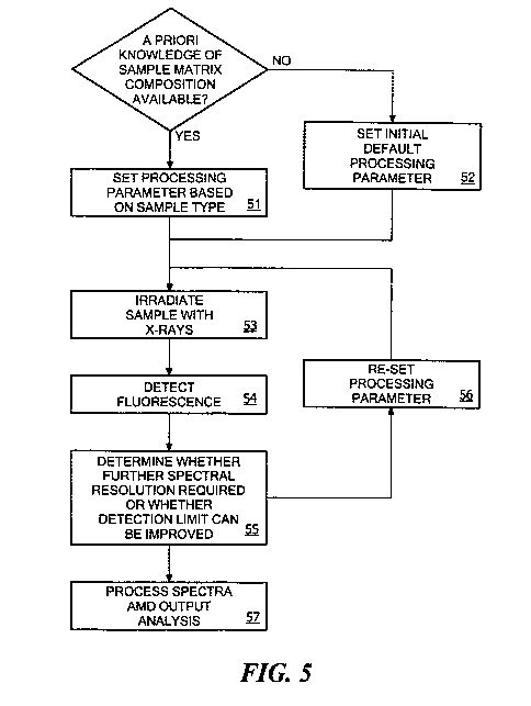
[00351 Embodiments of the present invention provide improved performance of
XRF analyzers by optimizing the pulse shaping time for a particular sample.
Referring
now to the flowchart of Fig. 5, when a priori knowledge of the sample matrix
is
available, the operator may select a sample type (e.g., via a touch-screen
interface) from a
list of candidate sample types, and the sample is then analyzed in accordance
with one or
more pre-stored processing parameters, such as pulse shaping time information
corresponding to the selected sample type, as indicated in step 51. In
instances where a
priori knowledge of the sample is not available, then the pulse shaping time,
initially set
to a default value (step 52) may be adaptively adjusted during an analysis
cycle based on
data acquired and processed early in the analysis cycle. More specifically,
the sample is
irradiated with a beam of x-rays generated, for example, by x-ray source 102
of FIG. 1 to
cause the emission of characteristic fluoresced x-rays by atoms in the sample,
step 53.
The detector receives the fluoresced x-rays and responsively produces pulses
representative of the energies and intensities of the x-rays, step 54. The
pulses produced
by the detector are shaped in accordance with the pulse processing parameters
set in steps
51 or 52. The processed pulses are conveyed to the controller, which analyzes
the
accumulated pulses to create an energy spectrum of the detected x-rays. This
analysis of
the processed pulses and generation of the energy spectrum occurs in real-
time, i.e.,
substantially concurrently with the irradiation/detection steps. As the energy
spectral data
9
CA 02741366 2011-04-20
WO 2010/054018 PCT/US2009/063311
are accumulated, the controller analyzes the data to determine whether
components of
the spectrum meets targeted performance criteria, for example energy
resolution or count
rate, step 55. If the controller determines that the targeted performance
criteria are not
satisfied, then the pulse processing parameter(s) is or are adjusted so as to
achieve
satisfactory performance; for example, the pulse shaping time applied to the
detector
pulses may be increased to improve energy resolution, step 56. The analysis
cycle,
consisting of irradiation, detection and spectrum acquisition, is then
continued at the
adjusted pulse processing parameters, step 57, in accordance with stored
instructions. It
should be noted that the changed energy resolution of the detector arising
from the
adjusted pulse processing parameter(s), and the energy calibration of the
detector, must
be factored into the real-time analysis of the data. The adjustment algorithm
is
programmed into the DSP since, for a given model of detector, the energy
resolution and
energy calibration of a pulse processing system is a fixed function of the
pulse processing
parameters. The analysis cycle will typically terminate after a specified time
period or
when certain spectrum characteristics (e.g., signal-to-noise ratios) have been
achieved or
when the statistical uncertainties of the elemental concentrations have
reached a
predetermined level.
[00361 The embodiments of the invention described above are intended to be
merely exemplary; numerous variations and modifications will be apparent to
those
skilled in the art. All such variations and modifications are intended to be
within the
scope of the present invention as defined in any appended claims.