Note: Descriptions are shown in the official language in which they were submitted.
CA 02741397 2011-05-24
f
NANOSTRUCTURES AND METHODS FOR
MANUFACTURING THE SAME
BACKGROUND OF THE INVENTION
Field of the Invention
This invention relates generally to structures, essentially in one-dimensional
form, and which are of nanometer dimensions in their width or diameter, and
which
are commonly known as nanowhiskers, nanorods, nanowires, nanotubes, etc.; for
the
purposes of this specification, such structures will be termed "one-
dimensional
nanoelements". More specifically, but not exclusively, the invention relates
to
nanowhiskers, and to methods of forming nanowhiskers.
Brief Description of the Prior Art
The basic process of whisker formation on substrates, by the so-called VLS
(vapor-liquid-solid) mechanism is well known. A particle of a catalytic
material,
usually gold, for example, on a substrate is heated in the presence of certain
gases to
form a melt. A pillar forms under the melt, and the melt rises up on top of
the pillar.
The result is a whisker of a desired material with the solidised particle melt
positioned
on top -see "Growth of Whiskers by the Vapour-Liquid-Solid Mechanism"-
Givargizov - Current Topics in Materials Science Vol. 1, pages 79-145-North
Holland
Publishing Company 1978. The dimensions of such whiskers were in the
micrometer
range.
International Application WO 01/84238 discloses in Figures 15 and 16 a
method of forming nanowhiskers wherein nanometer sized particles from an
aerosol
are deposited on a substrate and these particles are used as seeds to create
filaments or
nanowhiskers. For the purposes of this specification the term nanowhiskers is
intended to mean one dimensional nanoelements with a diameter of nanometer
CA 02741397 2011-05-24
dimensions, the element having been formed by the VLS mechanism.
Typically, nanostructures are devices having at least two dimensions less than
about I pm (i.e., nanometer dimensions). Ordinarily, layered structures or
stock
materials having one or more layers with a thickness less than 1 pm are not
considered to be nanostructures, although nanostructures may be used in the
preparation of such layers, as is disclosed below. Thus the term
nanostructures
includes free-standing or isolated structures having two dimensions less than
about
1 gm which have functions and utilities that are different from larger
structures and
are typically manufactured by methods that are different from conventional
procedures for preparing somewhat larger, i.e., microscale, structures. Thus,
although
the exact boundaries of the class of nanostructures are not defined by a
particular
numerical size limit, the term has come to signify such a class that is
readily
recognized by those skilled in the art. In many cases, an upper limit of the
size of the
dimensions that characterize nanostructures is about 500 nm.
Where the diameter of a nanoelement is below a certain amount, say 50nm,
quantum confinement occurs where electrons can only move in the length
direction of
the nanoelement; whereas for the diametral plane, the electrons occupy quantum
mechanical eigenstates.
The electrical and optical properties of semiconductor nanowhiskers are
fundamentally determined by their crystalline structure, shape, and size. In
particular,
a small variation of the width of the whisker may provoke a considerable
change in
the separation of the energy states due to the quantum confinement effect.
Accordingly, it is of importance that the whisker width can be chosen freely,
and, of
equal importance, is that the width can be kept constant for extended whisker
lengths.
This, together with the possibility of positioning whiskers at selected
positions on a
substrate, will be necessary if an integration of whisker technology with
current
semiconductor component technology is to be possible. Several experimental
studies
on the growth of GaAs whiskers have been made, the most important reported by
Hiruma et al. They grew III-V nano-whiskers on III-V substrates in a metal
organic
chemical vapor deposition -MOCVD- growth system - K. Hirunza, M. Yazawa, K.
Haraguchi, K. Ogawa, T. Katsuyama, M.Koguchi, and H. Kakibayashi, J. Appl.
Phys.
74, 3162 1993; K. Hirurna, M. Yazawa, T. Katsuyama, K. Ogawa, K. Haraguchi,
.2-
CA 02741397 2011-05-24
M.Koguchi, and H. Kakibayashi, J. Appl. Phys. 77,4471995 ; E. I. Givargizov,
J.
Cryst. Growth 31,20 1975; X. F. Duan, J. F. Wang, and C. M. Lieber, Appl.
Phys.
Lett. 76, 1116 2000; K. Hirunza, H. Murakoshi, M. Yazawa, K. Ogawa, S.
Fukuhara,
Al. Shirai,and T. Katsuyarna, IEICE Trans. Electron. E77C, 1420 1994; K.
Hirurna,
et al, "Self-organised growth on GaAs/InAs heterostructure nanocylinders by
organometallic vapor phase epitaxy", J. Crystal growth 163, (1996), 226 - 231.
Their approach relied on annealing a thin Au film to form the seed particles.
In this
way, they achieved a homogeneous whisker width distribution, the mean size of
which could be controlled by the thickness of the Au layer and the way this
layer
transforms to nanoparticles. With this technique, it is difficult to control
the size and
surface coverage separately, and it is virtually impossible to achieve a low
coverage.
The correlation between film thickness and whisker thickness was not
straightforward, since the whisker width also depended on growth temperature,
and
there were even signs of a temperature-dependent equilibrium size of the An
particles.
The authors also noticed a strong correlation between the size of the An
droplets de-
posited from a scanning tunneling microscope tip and the resulting whisker
width. For
the free-flying Si whiskers grown by Lieber et al.,- Y. Cui, L. J. Lauhon, M.
S.
Gudiksen, J. F. Wang, and C. M. Lieber, Appl.Phys. Lett. 78, 2214, 2001 - a
clear
particle-whisker size correlation has been shown.
It is necessary, if whiskers are to be used as electrical components, that
there
should be well-defined electrical junctions situated along the length of a
whisker, and
much work has been directed at achieving this - see for example Hiruma et al,
"Growth and Characterisation of Nanometer-Scale GaAs, AlGaAs and GaAs/InAs
Wires" IEICE Trans. Electron., Vol. E77-C, No.9 September 1994, pp 1420-1424.
However, much improvement is necessary.
Much work has also been carried out on carbon nanotubes (CNTs). Despite
progress, research has been frustrated by a lack of control of the
conductivity-type of
CNTs and an inability to form 1D heterostructures in a controlled manner.
Randomly
formed interfaces as kinks between metallic and semiconducting parts of CNTs
have
been identified and studied (Yao et al, Nature, 1999, 402, 273) as have doping
(pn)
junctions in semiconducting CNTs (Derycke et al, Nano Letters, 2001, 1,453)
and
-3-
CA 02741397 2011-05-24
transitions between CNTs and semiconductor (Si and SiC) nanowhiskers (Hu et
al,
Nature, 1999, 399, 48).
In a separate trend of development, attempts to fabricate ID devices have been
made since the late 1980s by top-down methods, as pioneered by Randall, Reed
and
co-workers at Texas Instruments - M.A. Reed et al., Phys. Rev. Lett. 60,
535(1988).
Their top-down approach, which still represents the state of the art for this
family of
quantum devices, is based on epitaxial growth of multi-layers defining the two
barriers and the central quantum well. Electron-beam lithography is then used
to
define the lateral confinement pattern, together with evaporation of the
metallic layers
to form the top contact. A lift-off process is then used to remove the e-beam-
sensitive
resist from the surface, and reactive ion etching removes all the material
surrounding
the intended narrow columns. Finally, the devices are contacted via the
substrate and
from the top using a polyimide layer. In the studies of devices fabricated by
this
bottom-up technique, 100-200 nm diameter columns have been observed, however,
with rather disappointing electrical characteristics and peak-to-valley
currents at best
around 1.1:1. An alternative approach to realizing low-dimensional resonant
tunneling devices has been reported more recently, employed strain-induced
formation of self-assembled quantum dots (I.E. Itskevich et al., Phys. Rev. B
54,
16401(1996); M. Narihiro, G. Yusa, Y_ Nakamura, T. Noda, H. Sakaki, Appl.
Phys.
Lett. 70, 105(1996); M. Borgstrom et al., Appl. Phys. Lett. 78, 3232(2001)).
SUMMARY OF THE INVENTION
The invention comprises a method of forming nanowhiskers, one-dimensional
semiconductor nanocrystals, in which segments of the whisker have different
compositions, for example indium arsenide whiskers containing segments of
indium
phosphide, wherein conditions for growth allow the formation of abrupt
interfaces and
heterostructure barriers of thickness from a few monolayers to hundreds of
nanometers, thus creating a one-dimensional landscape along which electrons
can
move. In a preferred method of chemical beam epitaxy method (CBE), rapid
alteration of the composition is controlled by the supply of precursor atoms
into a
eutectic melt of seed particle and substrate, supplied as molecular beams into
the ultra
high vacuum chamber. The rapid switching between different compositions is
-4-
CA 02741397 2011-05-24
obtained via a sequence where growth is interrupted or at least reduced to an
insignificant amount, and supersaturation conditions for growth are
reestablished; at
least, change of composition and supersaturation is changed faster than any
appreciable growth. With abrupt changes in material of the whisker, stresses
and
strains arising from lattice mismatch are accommodated by radial outward
bulging of
the whisker, or at least by lateral displacement of the atoms in the lattice
planes near
the junction.
Further, the invention includes a technique for the synthesis of size-
selected,
epitaxial nano-whiskers, grown on a crystalline substrate. As catalysts, size-
selected
gold aerosol particles are used, which enables the surface coverage to be
varied
completely independently of the whisker diameter. The whiskers were rod
shaped,
with a uniform diameter between 10 and 50 rim, correlated to the size of the
catalytic
seed. By the use of nano-manipulation of the aerosol particles, individual
nano-
whiskers can be nucleated in a controlled manner at specific positions on a
substrate
with accuracy on the rim level. The method of the invention enhances width
control
of the whisker by virtue of choice of nanoparticle. The nanoparticle may be an
aerosol
or a liquid alloy on the substrate may be made by starting from gold
rectangles
formed on the substrate which when melted form accurate diameter balls. Other
materials may be used instead of gold as the seed particle, e.g. Gallium.
Whilst it is desirable in many applications to have nanowhiskers which are
essentially constant in diameter, the shape of the whisker, and other
attributes, may be
varied by selectively changing the diffusion constant (diffusion coefficient)
of the
group III material, e.g. Ga, during whisker formation. This can be done by:
= Lowering the temperature of the process- this produces whiskers
tapered towards their free ends;
= Increasing the pressure of the group V material;
= Increasing the pressure of both group V and group III materials.
More specifically, the invention provides a method of forming a nanowhisker
comprising:
depositing a seed particle on a substrate, and exposing the seed particle to
materials under controlled conditions of temperature and pressure such as to
form a
melt with the seed particle, so that the seed particle melt rises on top of a
column
-5-
CA 02741397 2011-05-24
whereby to form a nanowhisker, the column of the nanowhisker having a diameter
with a nanometer dimension;
wherein during the growth of the column, selectively changing the
compositions of said materials whereby to abruptly change the composition of
the
material of the column at regions along its length, whilst retaining epitaxial
growth,
whereby to form a column having along its length at least first and second
semiconductor segment lengths, the first semiconductor segment being of a
material
having a different band gap from that of the second semiconductor segment.
Functional 1D resonant tunneling diodes and other components and structures
have been obtained via bottom-up assembly of designed segments of different
semiconductor materials in III/V nanowhiskers. Electronic and photonics
components
comprising nanowhiskers have also been formed as heterostructures, with a
single
crystal formation, wherein length segments of the nanowhisker are of different
materials, so as to create well defined junctions in the whisker between
different band
gap materials, whereby to create a component with a desired function.
Thus, the invention provides in general terms a heterostructure electronic or
photonics component, comprising a nanowhisker having a column of a diameter
with
a nanometer dimension, the column having disposed along its length a plurality
of
length segments of different material composition with predetermined diametral
boundaries between adjacent segments extending over a predetermined length of
the
nanowhisker column, such as to give desired band gap changes at the
boundaries, in
order to enable the component to carry out a desired function.
In a general aspect, the invention provides an electronic or photonic
component, comprising a nanowhisker having a column with a diameter, which has
a
nanometer dimension,
the column comprising along its length at least first and second length
segments of different materials with an abrupt epitaxial composition boundary
disposed between the first and second segments, wherein lattice mismatch at
the
boundary is accommodated by radial outward expansion of the nanowhisker at the
boundary.
-6-
CA 02741397 2011-05-24
In another general aspect, the invention provides an electronic or photonic
component, comprising a nanowhisker having a column with a diameter, which has
a
nanometer dimension,
the column comprising along its length at least first and second length
segments of different materials with an abrupt epitaxial diametral material
boundary
disposed between the first and second segments, wherein the transition between
the
composition of the different materials of the first and second segments occurs
over an
axial distance of not more than eight diametral lattice planes. Preferably,
the
transition between the composition of the first and second segment occurs over
an
axial distance of not more than 6, lattice planes, preferably not more than 5
lattice
planes, still more preferably not more than 4 lattice planes, still more
preferably not
more than 3 lattice planes, still more preferably not more than 2 lattice
planes and
most preferably not more than one lattice plane.
In a further aspect, the invention provides an electronic or photonic
component, comprising a nanowhisker having a column with a diameter which has
a
nanometer dimension, the column comprising along its length at least first and
second
length segments of different materials, the first segment having a
stoichiometric
composition of the form A1_,,B,,, and the second segment having a
stoichiometric
composition of the form AI_yBy, where A and B are selected substances, and x
and y
are variables, wherein an epitaxial composition boundary disposed between the
first
and second segments, comprises a predetermined gradual change from the
variable x
to the variable y over a predetermined number of diametral lattice planes. In
a similar
embodiment the compositions of the first and second segments of a nanowhisker
of
the invention can be represented by the formulas A,_,,BXC, and A1_yByC,
respectively,
wherein A and B represent elements of one group, e.g., group III, of the
periodic
table, and C represents an element of another group, e.g., group V, of the
periodic
table. The variables x and y may assume a value between 0 and 1, and represent
different numbers within that range. Thus, such a nanowhisker is formed of a
compound semiconductor that may vary in composition along its length, thereby
3 0 incorporating a heterojunction. An example of such a compound
semiconductor is
Al,,Gai.,As. A nanowhisker of the invention may be constructed to have, e.g.,
two
lengthwise segments, a first segment having a composition Al1_xGa.,As, wherein
the
-7-
CA 02741397 2011-05-24
variable x has a given value between 0 and 1 and a second segment having a
composition Alr_yGayAs, wherein the variable y has a second value different
from the
value of x. Between the two segments is an interface within which the
composition
varies continuously from the composition of the first segment to that of the
second
segment, i.e., the value of the variable x changes continuously, and usually
monotonically, to the value of the variable y. This interface thus constitutes
a
heterojunction. The transition may be made to occur over a predetermined
number of
diametral lattice planes by adjusting the conditions under which the whiskers
are
grown, as will be explained in more detail below. Furthermore, the growth
conditions
can be periodically adjusted to produce a plurality of such heterojunctions
along the
length of the nanowhisker.
The diameter of the nanowhisker is controlled by the invention to be
essentially constant along the length of the nanowhisker, or having a defined
variation, such as a controlled taper. This ensures precise electrical
parameters for the
nanowhisker, the controlled taper being equivalent to producing a voltage
gradient
along the length of the nanowhisker. The diameter may be small enough such
that the
nanowhisker exhibits quantum confinement effects- Although the diameter is
precisely controlled, there will be small variations in the diameter arising
from the
processing method, in particular a radial outward bulging of the nanowhisker
at a
composition boundary in order to accommodate lattice mismatch in the epitaxial
structure. In addition the diameter of one segment may be slightly different
from that
of another segment of a different material, because of the difference in
lattice
dimensions.
According to the invention the diameter of the nanowhiskers preferably will
not be greater than about 500 nm, preferably not greater than about 100 nm,
and more
preferably not greater than about 50 nm_ Furthermore, the diameter of the
nanowhiskers of the invention may preferably be in a range of not greater than
about
20 nm, or not great than about 10 rim, or not greater than about 5 nm.
The precision of formation of the nanowhisker enables production of devices
relying on quantum confinement effects, in particular a resonant tunneling
diode.
Thus, an RTD has been developed wherein the emitter, collector and the central
quantum dot are made from InAs and the barrier material from InP. Ideal
resonant
-8-
CA 02741397 2011-05-24
tunneling behavior, with peak-to-valley ratios of up to 50:1, was observed at
low
temperatures.
In a specific aspect, the invention provides a resonant tunneling diode,
comprising a nanowhisker having a column of a diameter with a nanometer
dimension, such as to exhibit quantum confinement effects,
the column comprising along its length first and second semiconductor length
segment forming respectively an emitter and a collector, and, disposed between
the
first and second semiconductor segments, third and fourth length segments of
material
having a different band gap from that of the first and second semiconductor
segments,
and a fifth central length segment of a semiconductor material having a
different band
gap from that of the third and fourth segments, disposed between the third and
fourth
segments and forming a quantum well.
A problem which arises with an electrical or photonic component formed from
a nanowhisker is that of making efficient electrical contacts to the
nanowhisker.
One method is to remove the nanowhisker from its substrate, by a mechanical
scraping process, and to deposit the nanowhiskers on a further substrate, on
their side
lengthwise on the substrate. Metallised bond pads may then be formed over the
ends
of the nanowhisker, or alternatively the nanowhisker can be manipulated to be
positioned over preformed contact pads.
Alternatively, in a method which may be better suited to mass-production, the
nanowhiskers may be left on the substrate, with their base ends having been
formed
on an electrical contact. Once formed, the nanowhiskers may be encapsulated in
a
resin or glassy substance, and then contact pads may be formed over the
surface of the
encapsulation in contact with the free ends of the nanowhiskers. To assist in
this, the
catalytic particle melt, towards the end of the formation of the nanowhisker,
may have
extra conductive substances injected into it, so as to improve the electrical
contact
with the bond pads.
Further specific components are set forth in the appended claims, and
described
below. In particular, these include a heterobipolar transistor, and light
emitting diodes
and photodetectors.
-9-
CA 02741397 2011-05-24
Light emitting diodes are well suited to the present invention, since it is
possible
to construct them with an emission wavelength which can be selected at will
from a
continuous range of wavelengths over the UV, visible, and infrared regions.
The present invention provides a light emitting diode, comprising a
nanowhisker having a column of a diameter with a nanometer dimension, such as
to
exhibit quantum confinement effects,
the column comprising along its length in sequence first, second and third
semiconductor length segments comprising respectively an emitter, quantum well
active segment and collector, said second segment having a different band gap
from
that of the first and second segments, and forming an active area of the light
emitting
diode.
One particular application of a light emitting diode is for emission of single
photons. This is of use in various applications, but in particular in quantum
cryptography, where unauthorised interception of a photon stream will
inevitably
cause destruction or modification of the photon, in accordance with quantum
theory,
and thus corruption of the transmitted signal - see P. Michler, A. Imamoglu,
M. D.
Mason, P.J. Carson, G. F. Strouse, S. K. Buratto, Nature 406, 968 (2000); C.
Santori,
M. Pelton, G. Solomon, Y. Dale, Y. Yamamoto, Phys. Rev. Lett. 86, 1502 (2001).
The invention provides a single photon light source, comprising a one
dimensional nanoelement, having disposed along its length a volume of
optically
active material sufficiently small to form a quantum well, with tunneling
barriers
formed on either side of the quantum well, such that in use the quantum well
is
capable of emitting a single photon at a time.
Another form of light source in accordance with the invention is designed for
terahertz radiation, beyond the far infrared. Much work has been done on
superlattices, pioneered by Capasso and co-workers at Lucent Technologies.
Their
'quantum cascade' lasers utilise intersubband photon emission in
InGaAs/InAlAs/InP
heterostructures, and have achieved room temperature (pulsed mode) operation
at
wavelengths up to 17 microns. See for example IEEE Spectrum July 2002, pages
23,24,"Using Unusable Frequencies" and F. Capasso, C. Gmachl, D. L. Sivco, and
a.
Y. Cho, "Quantum cascade lasers" Physics Today, May 2000, pp. 34-39.
-10-
CA 02741397 2011-05-24
The invention provides a source of terahertz radiation, comprising a
nanowhisker having a column of a diameter with a nanometer dimension, the
column
including a multiplicity of layers of a first band gap semiconductor
interleaved with a
multiplicity of layers of a second band gap material, whereby to form a
superlattice,
the dimensions being such that electrons can move with a wave vector such as
to
radiate terahertz radiation.
In components, structures and processes according to the invention, an array
of
a large number of nanowhiskers may be formed extending from a substrate,
essentially parallel to one another. There are various methods of forming such
arrays,
for example positioning an array of aerosol particles on the substrate to
provide
catalytic seed particles, depositing particles on the substrate from a
colloidal solution,
or forming on the substrate by a nanoimprint lithography (NIL) process (or by
any
other lithography process, e.g. e beam, UV, or X-ray), an array of areas of
predetermined shape (rectangular or other shape) and thickness, which when
heated,
form balls of a desired volume to permit the nanowhisker growth process to
proceed.
Such arrays may be employed as photonic crystals, solar cells comprised of a
large number of photodetectors, field emission displays (FED), converters to
convert
an infrared image to a visible light image, all as described herein below. A.
further
application is that of a polarisation filter.
In processes of the invention, an array of a large number of nanowhiskers may
be employed to create a layer of an epitaxial material on a wafer substrate of
a
cheaper substance, for example silicon. A long-standing problem in the art is
the
formation of single crystal wafers of expensive III-V materials, from which
chips can
be formed. Much research has been made into forming single crystal layers on
silicon
wafer substrates - see for example WO 02/01648. However further improvements
are
desirable.
In accordance with the invention, a substrate of silicon or other substance is
provided on which is grown a mask material, resistant to epitaxial growth, for
example a dielectric material such as SiO?, or Si3N4 . An array of nanometer-
dimensioned apertures is formed in the mask material, such as by a NIL
process, and
catalytic seed-forming material is deposited in the apertures- Alternatively
an array of
seed for iing material areas is deposited on the substrate, and a layer of
mask material
-11-
CA 02741397 2011-05-24
is then deposited over the substrate and the seed particle areas. Application
of heat
causes melting of the seed particle areas to create the seed particles, and
then growth
of the nanowhiskers of the desired III-V or other material is initiated. After
growth of
the nanowhiskers, growth of the desired material continues, using the whiskers
as
nucleation centres, until a single continuous layer of the material is formed.
The
material is single crystal epitaxial. As preferred, the seed particle melt at
the end of
the nanowhiskers is removed at a convenient opportunity to avoid contamination
of
the epitaxial layer.
In a modification, mass growth of the epitaxial layer is initiated, using the
seed
particle melts as nucleation points, prior to formation of the nanowhiskers,
and while
the growth underneath the seed particles is still in the liquid phase.
In a further modification, microscopic V-grooves are formed in the upper
surface of the silicon surface, for example <111> etchings in a <100>
substrate. The
seed particle forming areas are formed on the surfaces of the V-grooves,
whereby the
nanowhiskers grow at an angle to the substrate, and cross one another at the
grooves.
This makes for a more efficient growth of the epitaxial layer from the
nanowhisker
nucleation centres. Further, grain boundaries between domain areas with
different
growth phases are avoided; which has been a problem with prior processes.
The present invention thus provides in a further aspect a method for forming
an
epitaxial layer of a desired material on a substrate of a different material,
the method
comprising forming on a substrate a configuration of seed particle material
areas,
forming a layer of mask material around the seed particle areas, growing
nanowhiskers from the seed particles areas of said desired material, and
continuing to
grow said desired material, using the nanowhiskers as growth sites, whereby to
create
an epitaxial layer of said desired material extending over said substrate.
In a further aspect of the invention, processes have been developed for
forming
nanowhiskers of III-V material extending in the <100> direction, as opposed to
the
usual <111> direction for nanowhiskers. This has important applications,
particularly
for nitride materials which tend to grow in the <111> direction, but with many
stacking faults, as the material alternates between a zinc blende and wurtzite
structure.
The invention provides a method of forming nanowhiskers comprising
providing a substrate, forming a configuration of seed particles on the upper
surface,
-12-
CA 02741397 2011-05-24
growing nanowhiskers from said seed particles which extend from the substrate
initially in a <111> direction, and forming a short segment of a barrier
material in said
nanowhiskers such as to change their direction of growth to a <100> direction.
In a further aspect, the invention provides method of forming nanowhiskers, a
method
of forming nanowhiskers, comprising providing a substrate, forming a
configuration
of seed particles on the upper surface, growing nanowhiskers from said seed
particles
which extend from the substrate initially in a <111> direction, and changing
the
growth conditions of said nanowhiskers such as to change their direction of
growth to
a <100> direction.
The present invention also relates to one-dimensional nanoelements
incorporated in
MEMS devices - micromechanical devices.
In one aspect a substrate, for example of silicon, has a matrix of electrical
contact areas formed on one surface. On each contact area, one, or a number,
of
nanowhiskers are formed from, for example, gold catalyst particles so as to be
upstanding from the substrate's surface. Each nanowhisker, or group of
nanowhiskers
may therefore be individually addressable by electrical signals. Such a
structure may
make contact with the end of a nerve or perhaps the nerves in the retina of an
eye, and
the electrodes may be' activated so as to provide a repairing or artificial
function for
enabling the nerve. Thus for example, when applied in the retina of an eye,
the
structure may overcome certain blindness problems.
In another aspect a nanowbisker is provided, which may function as a nerve
electrode or in other applications, wherein the whisker is formed of silicon
or of a
metal which may be oxidised, and the whisker is oxidised to form a layer of
oxide
along its length. The particle melt at the end of the whisker however
including gold
or other non- oxidisable material remains free of oxide and may therefore be
used to
form an electrical contact. This arrangement provides more precise electrical
characteristics than nanowhiskers with exposed conductive material along their
lengths and such nanowhiskers may be used as nerve electrodes or as devices
where
the capacitance of the nanowhisker is of importance. As an alternative, other
materials may be used as the outer layer for example higher bandgap shells,
for
example where the whisker is formed of gallium arsenide, the outer layer may
be
gallium phosphide.
-13-
CA 02741397 2011-05-24
An important application of nanostructures is in micromechanical cantilever
beams where a beam fixed at one end projects into space and may be subject to
an
external force, for example, electrical or weight or an external object or a
chemical
force, to give a bending of the cantilever. This bending may be detected for
example
by a change in electrical capacitance of the structure.
In a further aspect the present invention provides one or more nanowhiskers,
which may or may not be oxidised in accordance with the above-mentioned aspect
of
the invention along their length to provide a cantilever or an array of
cantilevers
formed as a row or parallel beams. Such an arrangement may provide an order of
magnitude or more sensitivity than a previous arrangement where an etching
process
has been used to produce the beams.
One application for such cantilevers is where the whiskers are formed with a
material with a coating which is sensitive to certain organic molecules or
biological
molecules, such that a molecule, when making contact with a cantilever beam
undergoes a certain chemical reaction. This produces certain stresses on the
cantilever beam and causes bending of the beam, which may be detected by
optical or
electrical monitoring.
In a further specific aspect, a nanowhisker is formed on a substrate
projecting
up into an aperture of a layer of material, which is essentially insulative.
The upper
surface of the insulative layer has an electrically conductive material formed
thereon.
This electrically conductive material is roughly the same height from the
substrate as
the tip of the nanowhisker, which has a conductive seed particle melt thereon.
By
appropriate activation of the conductive material, the whisker may be made to
mechanically vibrate within the aperture at a certain eigen frequency, for
example, in
the gigahertz range. During the period of a single vibration, a single
electron is
transferred from one side of the conductive material to the other via the seed
particle
melt. This creates a current standard generator, where the current I through
the
conductive material is equal to product of the frequency of vibration and the
charge e
of an electron: I = f=e.
If the whisker is sensitised to attract molecules of a certain type, then the
deposition of a molecule onto the whisker will change the inertial
characteristics of
the whisker and therefore its natural frequency of vibration. This may
therefore be
14-
CA 02741397 2011-05-24
detected by electrical activation of the conductive material. This technique
may be
used to calculate the weight of a molecule to a very accurate degree.
BRIEF DESCRIPTION OF THE DRAWINGS
Preferred embodiments of the invention will be now be described merely by
way of example with reference to the accompanying drawings, in which:
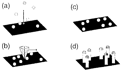
Figure 1 is a schematic depiction of a fabrication technique according to the
invention, for forming nanowhiskers: (a) deposition of size-selected Au
aerosol
particles onto a GaAs substrate; (b) AFM manipulation of the particles for the
positioning of the whiskers; (c) alloying to make a eutectic melt between Au
and Ga
from the surface; (d) GaAs whisker growth.
Figure 2. (a) TEM micrograph of GaAs nano-whiskers grown from 10 nm Au
aerosol particles. (b) SEM micrograph of a GaAs<lll>B substrate with GaAs
whiskers grown from 40 nm Au aerosol particles. (c) High-resolution electron
microscope image 400 kV of GaAs whisker grown from an Au cluster. The inset
shows a magnified part of the whisker.
Figure 3 is a schematic diagram of apparatus for carrying out the methods of
this invention.
Figure 4. Composition profile of an InAs nanowhisker, according to an
embodiment of the invention, containing several InP heterostructures, using
reciprocal
space analysis of lattice spacing. (a) High-resolution TEM image of a whisker
with a
diameter of 40 rim. (b) Power spectrum of the image in (a). (c) An inverse
Fourier
transform using the information closest to the InP part of the split 200
reflection. InP
(bright) is located in three bands with approximately 25, 8 and 1.5 nm width,
respectively. (d) Superimposed images, using an identical mask over the InP
and InAs
parts of the 200 reflection, respectively.
Figure 5. Analysis of InP heterostructures inside InAs nanowhiskers. (a) TEM
image of InP barriers (100, 25, 8, and 1.5 nm) inside a 40 nm diameter InAs
nanowhisker. (b) Magnification of the 8 nm barrier region, showing crystalline
perfection and the interface abruptness on the level of monolayers. (c)
Simulated
band-structure diagram of the InAs/InP heterostructures, including (left edge)
ideal
formation of ohmic contacts to InAs. (d) Ohmic I-V dependence for a
homogeneous
-15-
CA 02741397 2011-05-24
InAs whisker , contrasted by the strongly nonlinear I-V behavior seen, for an
InAs
whisker containing an 80 nm InP barrier . (e) Arrhenius plot showing
measurements
of thermionic excitation of electrons across the InP barrier (at a bias of 10
mV),
yielding a barrier height of 0.57 eV.
Figure 6. Evaluation of transport mechanisms for single barriers of various
thick nesses, for use in resonant tunneling diodes of the invention. (A) A SEM
image
of a whisker on the growth substrate. (Scale bar depicts 1 m.) (B) An
InAs/InP
nanowhisker contacted by two alloyed ohmic contacts. (Scale bar depicts 2 m.)
(C)
TEM image of an InAs whisker with an 8 nm InP segment perpendicular to the
long
axis of the whisker. (D) The current-voltage characteristics for three
different barrier
situations;
Figure 7. High-resolution TEM imaging. (A) A TEM image of an InAs
whisker grown in the <111> direction with two InP barriers for forming a first
embodiment of the invention. (Scale bar depicts 8 nm.) (B) A one-dimensionally
integrated profile of the boxed area in A. The width of the barrier is about
5.5 nm (16
lattice spacing), and the interface sharpness is of the order of 1-3 lattice
spacings,
judged by the jump in image contrast.
Figure 8. A resonant tunneling diode (RTD) forming an embodiment of the
invention.
(A) TEM image of the top end of a whisker with the double barrier clearly
visible, in this case with a barrier thickness of about 5 nm (scale bar
depicts 30 nm).
(B) The principle of the energy band diagram for the device investigated with
the characteristic electronic states in the emitter region indicated (left).
(C) Current-voltage data for the same device as shown in A and B revealing a
sharp peak in the characteristics, reflecting resonant tunneling into the
ground state,
Elz, with a voltage width of about 5 mV. This width can be translated into an
energy
width of the transition of about 2 meV, corresponding to the width of the
shaded
energy band in the emitter from which electrons tunnel. The device
characteristics are
shown in the inset, which provides a magnified view of the resonance peak for
increasing voltage and for decreasing voltage .
Figure 9 is a schematic representation of the preferred embodiment of the
resonant tunneling diode according to the invention;
-16-
CA 02741397 2011-05-24
Figure 10 is a schematic representation of a further embodiment of the
invention including a wide band gap insulating segment;
Figure II is a schematic representation of a further embodiment of the
invention comprising a hetero bipolar transistor (HBT);
Figure 12 is a band gap diagram of the HBT correlated with the HBT
structure;
Figure 13 is a diagram showing band gap variation with compositional change
of a ternary compound;
Figures 14A and 14B are diagrams showing band gap versus lattice
dimensions for a variety of semiconductor compounds;
Figure 15 is a schematic representation of an embodiment of the invention
comprising a light emitting diode and laser;
Figure 16 is a schematic representation of a further embodiment of the
invention comprising the application of a laser to detection of individual
molecules of
desired species;
Figure 17 is a schematic representation of a further embodiment of the
invention comprising the application of an array of lasers to patterning
photoresists in
a NIL process;
Figure 18A is a schematic representation of a further embodiment of the
invention comprising a photodetector, and Figures 18B and 18C are variants
thereof;
Figure 19A is a schematic representation of a further embodiment of the
invention comprising a solar cell, and Figure 19B is a variant thereof;
Figure 20 is a schematic representation of a further embodiment of the
invention
comprising a radiation source of terahertz radiation;
Figures 21A-C are schematic representations for explaining an embodiment of
the invention comprising a photonic crystal, and Figure 21D is a variant
thereof for
forming a 3-D photonics crystal;
Figures 22A-G are schematic representations of a further embodiment of the
invention for forming a layer of material epitaxial with a substrate, wherein
the
lattices are not matched to one another;
-17-
CA 02741397 2011-05-24
Figures 23A-C are schematic representations for explaining a further
embodiment of the invention for forming a layer of material epitaxial with a
substrate,
wherein the lattices are not matched to one another;
Figures 24A-B are schematic representations for explaining a further
embodiment of the invention, for forming whiskers, which extend in a<100>
direction, as opposed to the usual <l i l> direction;
Figures 25A-B are schematic representations of a further embodiment of the
invention comprising a field emission display (fed), wherein the individual
elements
of the display are nanowhiskers and are individually addressable;
Figure 26 is a schematic representation of a further embodiment of the
invention comprising an arrangement for upconverting an image in the infrared
region
to a visible light region;
Figure 27 is a schematic representation of a further embodiment of the
invention comprising an antenna for infrared radiation;
Figure 28 is a schematic representation of a further arrangement comprising a
ferromagnetic whisker for spintronics applications;
Figure 29 is a schematic view of a further embodiment of the invention
comprising an array of selectively addressable electrodes for implantation
into a
nerve;
Figure 30 is a schematic view of a further embodiment of the invention
comprising a nanowhisker with an oxidised outer surface along its length;
Figure 31 is a schematic view of a further embodiment comprising a row of
nanowhiskers upstanding from a substrate and forming a cantilever arrangement;
Figure 32 is a schematic view of a further embodiment of the invention
comprising a nanowhisker arranged for oscillation and providing precise
measurements of weight and frequency; and
Figure 33 is a schematic view of a further embodiment of the invention,
comprising the tip of a Scanning Tunneling Microscope.
DESCRIPTION OF THE PREFERRED EMBODIMENTS
Methods of producing nanowhiskers, in accordance with the invention will
now be described. Such methods may be suitable for production of resonant
-18-
CA 02741397 2011-05-24
tunneling diodes described below, and other electronic and/or photonic
components,
as will become apparent.
Whiskers are highly anisotropic structures, which are spatially catalyzed by
molten metallic droplets, often unintentionally introduced as contaminants, on
a
crystal surface. Gold is commonly chosen as catalyst, or seed particle, since
it forms
eutectic alloys with semiconductor materials or constituents such as Si, Ga,
and In.
The melting points of these eutectic alloys are lower than the usual growth
temperatures for Si and group III-V materials. The molten metal droplet serves
as a
miniature, liquid phase, epitaxy system, where precursors are fed into it in
the form of
a vapour or, in this case, by a molecular beam in vacuum. The growth is
usually
referred to as vapour-liquid-solid growth. The electrical and optical
properties of
semiconductor nanowhiskers are fundamentally determined by their crystalline
structure, shape, and size. In particular, a small variation of the width of
the whisker
provokes a considerable change in the separation of the energy states due to
the
quantum confinement effect. Accordingly, it is of importance that the whisker
width
can be chosen freely, and, of equal importance, is that the width can be kept
constant
for extended whisker lengths. This, together with the possibility of
positioning
whiskers at selected positions on a substrate, is necessary for an integration
of whisker
technology with current semiconductor component technology.
According to the invention, techniques have been developed for the synthesis
of size-selected, epitaxial nanowhiskers, grown on a crystalline substrate.
The
Chemical Beam Epitaxy apparatus employed in the techniques described below is
shown schematically in Figure 3.
Chemical Beam Epitaxy (CBE) combines a beam epitaxial technique like
Molecular Beam Epitaxy (MBE) and the use of chemical sources similar to Metal
Organic Chemical Vapor Deposition (MOCVD). In MOCVD or related laser ablation
techniques, the pressure inside the reactor is usually greater than 10 mbar
and the
gaseous reactants are viscous, which means that they have a relatively high
resistance
to flow. The chemicals reach the substrate surface by diffusion. CBE reduces
the
pressure to less than 10-' mbar and the mean free path of the diffusants then
becomes
longer than the distance between the source inlet and the substrate. The
transport
becomes collision free and occurs in the form of a molecular beam. The
exclusion of
-19-
CA 02741397 2011-05-24
the gas diffusion in the CBE system means a fast response in the flow at the
substrate
surface and this makes it possible to grow atomically abrupt interfaces.
The CBE apparatus shown in Figure 3 consists of a UHV (ultra-high vacuum)
growth chamber 1001 where the sample 1021 is mounted on a metal sample holder
1041 connected to a heater 1061. Around the chamber there is a ring 1081
filled with
liquid nitrogen that is called the cryoshroud. The cryoshroud pumps away
species
that don't impinge or that desorb from the substrate surface. It prevents
contamination of the growing surface layer and reduces the memory effect.
Vacuum
pumps 1101 are provided.
The sources 1121 for CBE are in liquid phase and they are contained in bottles
which have an overpressure compared to the chamber. The sources are usually as
follows: TMGa, TEGa, TMIn, TBAs, TBP. The bottles are stored in constant-
temperature baths and by controlling the temperature of the liquid source, the
partial
pressure of the vapor above the liquid is regulated. The vapor is then fed
into the
chamber through a pipe complex 1141 to, in the end of the pipe just before the
growth
chamber, a source injector 1161. The source injector is responsible for
injection of
the gas sources into the growth chamber 1001, and for generation of a
molecular
beam with stable and uniform intensity. The III-material, from the metal
organic
compounds TMIn (trimethylindium), TMGa (trimethylgallium) or TEGa
(triethylgallium), will be injected by low temperature injectors to avoid
condensation
of the growth species. They will decompose at the substrate surface. The V-
material
is provided by the metal-organic compounds, TBAs (tertiarybutylarsine) or TBP
(tertiarybutylphosphine). As opposed to the decomposition of the III-material,
the
V-material will be decomposed before injection into the growth chamber 1001,
at
high temperatures, in the injectors 1161. Those injectors 1161 are called
cracking
cells and the temperatures are kept around 900 C. The source beam impinges
directly
on the heated substrate surface. Either the molecule gets enough thermal
energy from
the surface substrate to dissociate in all its three alkyl radicals, leaving
the elemental
group III atom on the surface, or the molecule get desorbed in an
undissociated or
partially dissociated shape. Which of these processes dominates depends on the
temperature of the substrate and the arrival rate of the molecules to the
surface. At
-20-
CA 02741397 2011-05-24
higher temperatures, the growth rate will be limited by the supply and at
lower
temperatures it will be limited by the alkyl desorption that will block sites.
This Chemical Beam Epitaxy method permits formation of heterojunctions
within a nanowhisker, which are abrupt, in the sense there is a rapid
transition from
one material to another over a few atomic layers.
For the purposes of this specification, "atomically abrupt heterojunction", is
intended to mean a transition from one material to another material over two
or less
atomic monolayers, wherein the one material is at least 90% pure on one side
of the
two monolayers, and the other material is at least 90% pure on the other side
of the
two monolayers. Such "atomically abrupt heterojunctions" are sufficiently
abrupt to
permit fabrication of heterojunctions defining quantum wells in an electrical
component having a series of heterojunctions and associated quantum wells.
For the purposes of this specification, "sharp heterojunction", is intended to
mean a transition from one material to another material over five or less
atomic
monolayers, wherein the one material is at least 90% pure on one side of the
five
monolayers, and the other material is at least 90% pure on the other side of
the five
monolayers. Such "sharp heterojunctions" are sufficiently sharp to permit
fabrication
of electrical components having one, or a series of, heterojunctions within a
nanoelement, where the heterojunctions have to be accurately defined. Such
"sharp
heterojunctions" are also sufficiently sharp for many components relying on
quantum
effects.
As an illustration, in a compound AB used in the nanowhiskers of the
invention, where A represents one or more selected elements of a first group
and B
represents one or more selected elements of a second group, the total
proportions of
the selected element(s) in the first group and the selected element(s) in the
second
group are predetermined to constitute a semiconductor compound designed to
provide
desired properties. The compound AB is considered 90 % pure when the total
proportion of the selected element(s) within each group is at least 90 % of
its
predetermined proportion.
Example 1
Figures 1 and 3 show whiskers of predetermined sizes grown from several III-
V materials, in particular, GaAs whiskers with widths between 10 and 50 nm.
These
-21-
CA 02741397 2011-05-24
whiskers can be grown rod shaped with a uniform diameter, in contrast to
earlier
reports on epitaxially grown nano-whiskers, which tended to be tapered,
narrowing
from the base towards the top. As catalysts, size-selected gold aerosol
particles were
used, whereby the surface coverage can be varied independently of the whisker
diameter.
The whisker width in general is slightly larger than the seed particle
diameter.
This is mainly due to two factors: First, the gold particle incorporates Ga
and
possibly As from the substrate, which makes the particle grow. Second, when
the
particle melts, the base diameter of the liquid cap will be determined by the
wetting
angle between the alloy and the substrate surface. Simple assumptions give a
widening of up to 50%, depending on temperature and particle diameter, and
introduce a reproducible correlation between the particle diameter and the
width of
the whisker.
A GaAs<111>B substrate 10 was used, etched in HCL:H20, 1:10 to remove
any native oxide and surface contaminants before aerosol deposition. The size-
selected An particles 12 were made in a locally constructed aerosol facility
situated in
a glove box 14 with ultra pure N2 atmosphere. The particles are created in a
tube
furnace 16 by the evaporation/condensation method, at a temperature of about
1750 C, and are electrically charged by UV light at 18. The particles are size
selected
by means of a differential mobility analyzer DMA 20. The DMA classifies the
sizes
of charged aerosol particles by balancing their air resistance against their
mobility in
an electric field. After size classification, the particles were heated to 600
C, in order
to make them compact and spherical. The setup gives an aerosol flow with a
narrow
size distribution, the standard deviation being <5% of the mean particle
diameter. Still
charged, the particles were deposited on the substrate 10 by means of an
electric
field E. Size-selected aerosol particles in the range between 10 and 50 nm
were used
to grow whiskers.
After aerosol deposition, some samples were transferred to an AFM
Topometrix Explorer 24, also situated inside the glove box, and connected to
the
aerosol fabrication equipment. Thus, these samples were exposed only to sub-
ppm
levels of H2O and 02 during the deposition and manipulation phases. With the
AFM
-22-
CA 02741397 2011-05-24
tip, specific particles 12 were selected and placed in a predetermined
configuration,
giving complete control of the positioning of individual seed particles.
The GaAs substrate 10 with Au aerosol particles 12, either arranged or as
deposited, was then transferred into a chemical beam epitaxy CBE chamber. In a
CBE configuration, GaAs growth occurs under vacuum/molecular beam conditions
and with metal organic sources, in this case, triethylgallium TEG and
tertiarybutylarsine TBA. The TBA is thermally pre-cracked to predominantly As2
molecules, while the TEG usually cracks after impinging on the surface of the
substrate. The growth is typically performed with a slight As2 over-pressure,
which
means that the Ga flow determines the growth rate. Just before growth, the
substrate
was heated by a heater to 600 C for 5 min, while exposed to an As2 beam. In
this step,
the Au droplet can form an alloy with the GaAs constituents, whereby the Au
particle
absorbs some of the Ga from the substrate. The Au/Ga alloy forms at 339 C.
However, this step also works as a deoxidizing step, taking away any new
native
oxide layer, originating from the transport to and from the glove box system.
The
oxide is expected to evaporate at 590 C, although this is not always the case.
The
volatility of the oxide can be followed with reflective high-energy electron
diffraction
RHEED. With a successful transfer, a streaky diffraction pattern, indicating a
crystalline, reconstructed surface, can be seen already at temperatures .lower
than
500 C. Often, however, the oxide stays stable up to 590 C, sometimes as high
as
630 C. The whisker growth was performed at substrate temperatures between 500
and 560 C, with a TEG pressure of 0.5 mbar and a TBA pressure of 2.0 mbar.
After
growth, the samples were studied by scanning and transmission electron
microscopy
SEM and TEM.
The resulting whiskers were rod shaped and fairly homogeneous in size,
although their lengths varied slightly. The size homogeneity was clearly
dependent
on the volatility of the surface oxide. For samples with a hard oxide, as seen
with
RHEED, the size homogeneity was decreased. An oxygen-free environment is
therefore to be preferred for reproducible results. At the growth temperatures
described, no tapering of the whiskers was observed, irrespective of particle
size. For
whiskers grown below 500 C, however, there were clear signs of tapering. The
growth of either rod-shaped or tapered whiskers, depending on temperature, is
-23-
CA 02741397 2011-05-24
explained by the absence or presence of uncatalyzed growth on the surfaces
parallel to
the long axis of the whisker. The simplest surfaces of this orientation are
<110>
facets. Under ordinary CBE growth conditions, close to the ones used in these
experiments, <110> facets are migration surfaces. However, at lower
temperature,
the Ga diffusion constant decreases, which initiates growth on the <110>
facets. In
MOCVD growth the Ga migration length is even smaller, which explains the
typically
tapered whiskers of prior workers.
In Fig. 2a, a TEM image of a truss of 10 2-nm-wide whiskers grown from
nm particles is shown. The relatively low density of whiskers is illuminated
by the
10 SEM image in Fig. 2b, which is of a GaAs<l I l>B substrate with GaAs
whiskers
grown from 40 nm Au aerosol particles. In Fig. 2c, a single 40-rim-wide
whisker is
shown in a high-resolution TEM micrograph. The growth direction is
perpendicular
to the close-packed planes, i.e., 111. in the cubic sphalerite structure, as
found by other
groups. Twinning defects and stacking faults can also be observed, where the
whisker alternates between cubic and hexagonal structure. Most of the whisker
has
the anomalous wurzite structure W, except for the part closest to the Au
catalyst,
which always is zinc blende Z. SF = stacking fault, T=twin plane. The change
in
image contrast at the core is due to the hexagonal cross-section.
Such a growth method is used in the method described below with reference to
Figures 4 to 6 for forming whiskers with segments of the whisker with
different
compositions. The method is illustrated by InAs whiskers containing segments
of
InP.
Example 2
Conditions for growth of nanowhiskers allow the formation of abrupt
interfaces and heterostructure barriers of thickness from a few monolayers to
100s of
nanometers, thus creating a one-dimensional landscape along which the
electrons
move. The crystalline perfection, the quality of the interfaces, and the
variation in the
lattice constant are demonstrated by high-resolution transmission electron
microscopy, and the conduction band off-set of 0.6 eV is deduced from the
current
due to thermal excitation of electrons over an InP barrier.
In this method, the 111-V whiskers are grown by the vapor-liquid-solid growth
mode, with a gold nanoparticle catalytically inducing growth, in the manner
described
-24-
CA 02741397 2011-05-24
above. Growth occurs in an ultrahigh vacuum chamber 100, Figure 3, designed
for
chemical beam epitaxy (CBE). The rapid alteration of the composition is
controlled
by the supply of precursor atoms into the eutectic melt, supplied as molecular
beams
into the ultrahigh vacuum chamber. The rapid switching between different
compositions (e.g., between InAs and InP) is obtained via a sequence where
growth is
interrupted as the indium source (TMIn) is switched off, followed by a change
of the
group III sources. Finally, the supersaturation conditions, as a prerequisite
for
reinitiation of growth, are reestablished as the indium source is again
injected into the
growth chamber.
For the abruptness of the interfaces, Figure 4 shows TEM analysis of an InAs
whisker containing several InP heterostructure barriers. In Figure 4a, a high-
resolution image of the three topmost barriers is shown, recorded with a 400
kV
HRTEM (point resolution 0.16 nm). Figure 4b shows a nonquadratic power
spectrum
of the HREM image, showing that the growth direction is along [001] of the
cubic
lattice. The reflections show a slight splitting due to the difference in
lattice constants
between InAs and InP. Figure 4c shows an inverse Fourier transform, using a
soft-
edge mask over the part of the 200 reflection arising from the InP lattice. A
corresponding mask was put over the InAs part of the reflection. The two
images
were superimposed as in Figure 4d.
Figure 5a shows a TEM image of an InAs/InP whisker. The magnification of
the 5 nm barrier in Figure 5b shows the atomic perfection and abruptness of
the
heterostructure interface. Aligned with the 100 nm thick InP barrier, the
result of a
1D Poisson simulation (neglecting lateral quantization, the contribution of
which is
only about 10 meV) of the heterostructure 1D energy landscape expected to be
experienced by electrons moving along the whisker is drawn (Figure 5c). This
gives
an expected band offset (q'/4B) in the conduction band (where the electrons
move in
n-type material) of 0.6 eV. This steeplechase-like potential structure is very
different
from the situation encountered for electrons in a homogeneous InAs whisker,
for
which ohmic behavior (i.e., a linear dependence of the current (I) on voltage
(V)) is
expected and indeed observed (indicated curve in Figure 5d). This linear
behavior is
dramatically contrasted by the indicated I-V curve measured for an InAs
whisker
containing an 80 nm thick InP barrier. Strongly nonlinear behavior is
observed, with a
-25-
CA 02741397 2011-05-24
voltage bias of more than IV required to induce current through the whisker.
This
field-induced tunnel current increases steeply with increasing bias voltage,
as the
effective barrier through which the electrons must tunnel narrows. To test
whether
the ideal heterostructure band diagram within the 1D whisker is valid, the
temperature
dependence of the current of electrons overcoming the InP barrier via
thermionic
excitation was measured. The result is shown in Figure 5e, where the logarithm
of the
current (divided by T2) is plotted as a function of the inverse of the
temperature in an
Arrhenius fashion, measured at a small bias voltage (V) 10 mV) to minimize
band-
bending effects and the tunneling processes described above. From the slope of
the
line fitted to the experimental data points an effective barrier height,
ql/4B, of 0.57 eV
may be deduced, in good agreement with the simulation.
An added benefit of this approach to realizing heterostructures within ID
whiskers is the advantageous condition for combining highly mismatched
materials,
provided by the efficient strain relaxation by the proximity to the open side
surface in
the whisker geometry. In comparison, only a few atomic layers may be
epitaxially
grown in transitions between materials like InAs and InP with different
lattice
constants before either islanding or misfit dislocations occur, thereby
preventing
formation of ideal heterointerfaces.
Resonant Tunneling Diodes and Heterobipolar Transistors
The present invention also comprises, at least in preferred embodiments,
functional ID (one-dimensional) resonant tunneling diodes (RTDs) obtained via
bottom-up assembly of designed segments of different semiconductor materials
in
IEYV nanowires. Such RTDs comprise, in order, an emitter segment, a first
barrier
segment, a quantum well segment, a second barrier segment, and a collector
segment.
As is known to those skilled in the art, the barrier segments in RTDs are made
thin
enough that significant quantum tunneling of charge carriers is possible under
conditions that favor such tunneling. In RTDs according to the invention,
fabricated
in nanowitres, the nanowhiskers may be made thin enough so that the central
quantum
well is effectively a quantum dot.. In a concrete example, the emitter,
collector and
the central quantum dot may be made from InAs and the barrier material from
InP.
In an example, excellent resonant tunneling behavior, with peak-to-valley
ratios of up
to 50:1, was observed-
-26-
CA 02741397 2011-05-24
According to the invention ID heterostructure devices were fabricated
utilizing semiconductor nanowhiskers. The whiskers were grown by a vapor-
liquid-
solid growth mode, size controlled by, and seeded from, Au aerosol particles,
as more
fully described above in Examples 1 and 2. Growth takes place in a chemical
beam
epitaxy chamber under ultra-high-vacuum conditions where the supersaturation
of the
eutectic melt between the Au particles and the reactants acts as the driving
force for
whisker growth.
The incorporation of heterostructure segments into the whiskers is achieved
via the following switching sequence (more fully described above); the group
Ill-source beam is switched off to stop growth, and shortly thereafter the
group
V-source is changed. Once the group III-source is reintroduced into the
chamber, the
supersaturation is re-established and growth continues. In examples described
below
the material system used was InAs for the emitter, collector and dot, and InP
as the
barrier material. The aerosol particles were chosen so that the final whisker
diameter
was 40-50 nm. In order to prepare contacted electronic devices with single
nanowhiskers as the active elements, the whiskers were transferred from the
growth
substrate to a Si02-capped silicon wafer, on top of which large bond pads were
predefined by Au metal evaporation through a transmission electron microscope
(TEM) grid mask. In Fig. 6B a scanning electron microscope (SEM) image of a
nanowire device is shown, displaying the alignment capability in the e-beam
lithography system, allowing positioning of metallic electrodes on the
nanowires with
an accuracy that is better than 100 rim. Figure 6D shows the current-voltage
(I-V)
characteristics of a set of single-barrier devices, as the thickness of the
InP barrier was
varied from 80 nm down to zero. The thicker InP segments act as ideal
tunneling
barriers for electron transport, allowing only thermal excitation over this
barrier
(measured to be about 0.6 eV (23)) or tunneling made possible by the effective
thinning of the barrier when a large bias is applied to the sample. In Fig.6D
it can be
seen that almost no current flows through the thick InP barrier. In samples
containing
thinner single barriers (Fig. 2C), quantum tunneling is possible and electrons
can
penetrate barriers thinner than about 10 nm in thickness. In the extreme case
with zero
barrier thickness, the I-V characteristics are perfectly linear down to at
least 4.2 K. In
order to verify the crystalline quality and to evaluate the abruptness of the
-27-
CA 02741397 2011-05-24
heterointerfaces high-resolution TEM investigations were performed. In Fig. 7A
a
magnification of a 5.5 nm thick InP barrier in a <111>-InAs nanowhisker is
shown,
where the (I 11) lattice planes can be clearly seen. From the integrated
profile of the
area in Fig. 7A the sharpness of the interfaces was determined to be 1-3
lattice
spacings. The average spacing between the lattice fringes in the lighter band
is
0.344 nm, corresponding well to dl11= 0.338 nm of InP. Figure 7B is a one-
dimensionally integrated profile of the boxed area in A. The width of the
barrier is
about 5.5 nm (16 lattice spacings), and the interface sharpness is of the
order of
1-3 lattice spacings, judged by the jump in image contrast. The background is
not
linear due to bend and strain contrast around the interfaces. The difference
in lattice
spacing between the InP and the InAs is 3.4%, which corresponds well with the
theoretical value of the lattice mismatch (3.3%).
Since the heterointerfaces were determined to be abrupt enough for making
high quality quantum devices, double-barrier resonant tunneling devices may
therefore be envisaged. A barrier thickness of about 5 nm was chosen. In Fig.
8A a
TEM image of such a double barrier device structure formed inside a 40 nm wide
nanowhisker can be seen. The barrier thickness is roughly 5 nm on either side
of the
15 nm thick InAs quantum dot. Below the TEM image (Fig. 8B) the energy band
diagram expected for the device is shown, with the longitudinal confinement
(z-direction) determined by the length of the dot and the lateral confinement
(perpendicular direction) depending on the diameter of the whisker. For this
device
only the lowest transverse quantized level was occupied (splitting of the
order of 5
meV), with the Fermi energy indicated, determining the highest occupied
longitudinal
states filled with electrons. In between the two InP barriers the fully
quantized levels
of the central quantum dot are, indicated, with the same sequence as
schematically
indicated in the emitter region for the transverse quantized levels, but with
a greater
splitting (of the order of 100 meV) between the longitudinal quantized states
in the
quantum dot and an approximate quantization energy for the ground state of
Elz=40
meV. At zero applied bias, the current should be zero since no electronic
states in the
emitter are aligned with any states in the central dot because of the
difference in
energy quantization between the dot and the emitter. As the bias is increased
the
states in the dot will move towards lower energy and, as soon as the lowest
dot-state
-28-
CA 02741397 2011-05-24
is aligned with the Fermi level, the current starts to increase (here the
Fermi level is
assumed to lie between the two lowest states in the emitter). When the dot-
state falls
below the energy level of the first emitter state the current again drops to
zero,
resulting in the characteristic negative differential resistance.
The electrical properties of this ID DBRT device are presented in Fig. 8C,
showing almost ideal I-V characteristics, as expected for such a device. The I-
V trace
shows no current below a bias of around 70 mV, corresponding to the bias
condition
for which electrons must penetrate both barriers plus the central InAs segment
to
move from the emitter to the collector. At a bias of about 80 mV a sharp peak
is seen
in the I-V characteristics, with a half-width of about 5 mV in bias (which can
be
translated into an energy sharpness of the resonance of about 1-2 meV). The
peak-to-
valley ratio of the 80 mV peak is extremely high, about 50:1, and was seen in
different samples investigated. After the deep valley, the current increases
again for a
bias of about 100 mV, with some unresolved shoulder features observed on the
rising
slope. Note that the I-V trace for increasing bias voltage coincides with that
for
decreasing bias voltage indicating that the device characteristics are highly
reproducible and exhibit negligible hysteresis effects. In addition, the 80 mV
appears
similarly in the reverse bias polarity. In this case the peak is only slightly
shifted
(5 mV) suggesting a high symmetry of the device structure. Accordingly, these
results report the investigation of the materials and barrier properties of
single
heterostructure barriers inside semiconductor nanowires, bridging the gap from
thick
barriers, for which only thermal excitation above the barrier is possible,
down to
single barrier thickness, for which tunneling through the barrier dominates.
With this approach one-dimensional, double-barrier resonant tunneling
devices have been prepared, with high-quality device properties, and an energy
sharpness of about I meV and peak-to-valley current ratio of 50:1.
Referring now to Figure 9, a preferred embodiment of a resonant tunneling
diode is shown, having a nanowhisker 40 extending between collector and
emitter
contacts 42, 44, 2 microns apart. First and second InAs portions 46, 48 of the
whisker
make electrical contact with respective contacts 42, 44. Barrier portions
50,52 of InP
separate a central quantum dot or quantum well portion of InAs, 54, from the
emitter
and collector portions. The length of the portion 54 is around 30 nm. The
precise
-29-
CA 02741397 2011-05-24
dimensions will be selected in dependence upon bandgap barrier height, etc.,
in order
to achieve appropriate quantum confinement.
The diode operates in the conventional way of RTDs; for an explanation of the
theory of operation; see, for example, Ferry and Goldnick, Transport in
Nanostructures, CUP 1999, pp 94 et seq.
In the RTD of Figure 9, the segments 50, 52 may be replaced by a wide band
gap insulating material, in the manner shown in Figure 10. Referring to Figure
10, an
embodiment is shown having an insulating segment. A germanium whisker 100 is
grown by the processes described above, having a short segment 102 of silicon.
Lattice mismatch is accommodated by radial outward expansion of the whisker.
This
silicon dot is oxidised by heat to give a large silicon dioxide spacer 104
within the
germanium whisker. This has an extremely stable large bandgap offset.
Aluminium
can be used instead of silicon. This embodiment can be used for example for
tunneling effects, in the embodiment of Figure 9.
As regards making electrical contacts with the collector and emitter portions
of the embodiment of Figure 9, this can be done in different ways. The whisker
may
be positioned across large metallised bond pads, as shown in Figure 9.
Alternatively,
the nanowhisker may be positioned on a substrate, its position identified by a
suitable
scanning method, and then bond pads may be formed over the ends of the whisker
by
a metallization process. Another alternative is to leave the nanowhisker
extending
from the substrate, where it makes contact at its base with an electrical
contact, to
encapsulate the whisker in a resin or glassy substance, and then form an
electrode
over the encapsulation, making electrical contact with the whisker tip. This
latter
method may be more suitable for integration with other electrical components
and
circuits.
Referring now to Figures 11 to 14, an embodiment of the invention is
disclosed which comprises a heterojunction bipolar transistor (heterobipolar
transistor; HBT); this differs from the conventional bipolar transistor in
that different
band gap materials are used in the transistor. For example, a nanowhisker 110
may
have an emitter segment 112 of GaP, connected to a base segment 114 of p-doped
Si,
which is in turn connected to an n-doped collector segment 116 of Si.
Metallisation
electrodes 118 make contact with the respective segments 112, 114, and 116-
-30-
CA 02741397 2011-05-24
Figure 12 shows a band gap diagram for the HBT. By reason of the relatively
wide
band gap of the emitter, minority current flow from the base to the emitter is
inhibited. The depletion area between the base and collector is characterized
by a
gradual change in doping from p-type to n-type. As an alternative, the base
and
collector may be formed of ternary or quaternary materials, being a
stoichiometric
composition, and the composition gradually changes over a large number of
lattice
planes, say 100 to 1000, to give the required depletion region field. Change
in energy
band gap with composition is shown in Figure 13 for the ternary mixture
A1,,Ga1_,;As.
Figure 14 shows variation in bandgap energy and lattice parameters for a
variety of III-V materials. It will be appreciated that with the method of
forming
nanowhiskers according to the invention, it is possible to form
heteroepitaxial
junctions of materials with widely different lattice parameters, e.g. GaN/AIP,
the
lattice mismatch being accommodated by radial bulging of the whisker.
Photonics Components
Referring to Figure 15, this shows schematically an extremely small LED
capable of single photon emission. Single photon emission is of importance,
for
example for quantum photography or detection of individual molecules of
molecular
species. A whisker 150 has anode and cathode outer regions 15.2 of indium
phosphide
either side of an inner region 156 formed of indium arsenide, so as to define
a
quantum well. Regions 152 are connected to respective anode and cathode
electrical
contacts, formed as metallisation areas 158. In contrast to planar devices,
where
because of the need for lattice matching and for relieving mismatch strain,
only
certain wavelengths are possible, an important point of this embodiment is
that the
wavelength of the LED is fully variable since the materials making up the
diode may
be of any desired composition to achieve a desired wavelength of emission (see
Figure 14 discussed above), since lattice mismatch is accommodate by radial
outward
bulging of the whisker. Since the materials may be stoichiometric
compositions, the
wavelength is continuously variable across the range from 1.5ev to 0.35ev. A
one-
dimensional structure requires much less processing than prior art layered
structures
and is made by a self-assembly process, with the whole structure between the
electrical contacts. If a laser construction is required, Fabry Perot (FP)
cleavage
planes 159 are formed spaced an appropriate distance apart. As an alternative,
-31-
CA 02741397 2011-05-24
regions 159 are formed as mirrors comprising superlattices. The superlattices
may be
formed as alternating sequences of InP/InAs, the sequence alternating over
segments
of only a few lattice planes, as is known to those skilled in the art.
LEDs, lasers, and other micro cavity structures are often fabricated with
gallium nitride (GaN). Whilst nitrides have a number of advantages,
particularly in
optics, problems with nitrides are that firstly they are filled with
dislocations and that
secondly there is a lack of suitable substrates (sapphire being one commonly
used
substrate). Whiskers can be made with defect-free nitrides, and there is not a
problem
of lattice matching to a substrate. A regular FP laser can be made, with the
structure
of Figure 15, with dimensions less than 300nm, preferably of the order of
100nm. It
is a bottom up structure, which is well suited to reading DVDs and writing
thereto.
Nitride systems are quite well suited for whisker growth.
The light source-emitting region 156 can be made as ;small as about 20nm3.
This represents an extreme example of a point source and can be used, as
indicated
schematically in Figure 16 to locally excite individual biological cells 160.
The light
source 156 provides a near field 162 (exponentially decaying) which excites
the cell
160 since the physical spacing between the light source and object is a
fraction of a
wavelength. It is of use in DNA sequencing, and, as shown, the source 156 may
be
mounted in a groove 164 of a glass capillary tube 166. The cell flows along
the tube
as part of a fluid mixture, and flows past the source 156.
Referring to Figure 17, this shows an embodiment of the invention adapted for
Nano Imprint Lithography (NIL), where an array 170 of whiskers 156, providing
point sources of light, are individually addressable by an energisation source
172.
The array is mounted on a carriage 174 movable over the surface of a resist
material
176. The carriage is movable in steps of 20nm, and at each step, the whiskers
156 are
selectively energised in order to illuminate the material 176 with near field
light, and
to create a desired developable pattern in the resist 176.
Referring to Figure 18A, a photodetector is shown in accordance with the
invention. For example, a nanowhisker 180 may extend between metallised
contact
pads 182. There is typically a high contact resistance, between I OKf to 1
OOK.Q,
arising from small contact areas between padsl82, and whisker 180. The whisker
may comprise an n-doped indium phosphide portion 184, and a p-doped indium
-32-
CA 02741397 2011-05-24
phosphide portion 186, with a p-n junction 188 between, which may be abrupt,
or
may extend over a large number of lattice planes. This arrangement is suitable
for
detecting light with wavelengths 1.3 micron or 1.55 microns. As indicated in
Figure
14, any desired compositional "match" may be used, and therefore the materials
can
be modified for detection of any wavelength, from 1.55 microns or less. As an
alternative, a PIN or Schottky diode structure may be used. A PIN structure,
as
shown in Figure 18B has an intrinsic semiconductor material segment 188
between
the two semiconductor portions 184 and 186. The whisker is constructed as
described
with reference to Figure 10. A Schottky diode structure, as shown in Figure
18C has
a base portion 189 formed as a metallisation contact from which the whisker
extends;
the interface between the contact and the whisker forms the Schottky diode.
The
lower frequency limit on detection of radiation is in the terahertz region of
the
electromagnetic spectrum.
Referring to Figure 19A, a solar cell application is shown for the
photodetector structures of Figure 18. Millions of whiskers 190, each having p-
and
n-doped portions 191, 192 are formed on a substrate 193, doped (P+). The
whiskers
are formed by growth using gold, or other, nanoparticles, deposited onto
substrate
193, e.g., from an aerosol. The whiskers may be encapsulated in plastics 194
and
have a transparent tin oxide electrode 196 on the upper surface, which makes
contact
with the free ends of the whiskers to permit electrical current to flow along
the length
of the whiskers. The structure is extremely efficient in trapping light since
each
whisker is 100% reliable. The overall efficiency is between 35 and 50% and is
of use
in multi-bandgap solar cells. By contrast amorphous silicon grown at 300 C
gives an
efficiency of about 10%. Crystalline silicon gives an efficiency of about 15%
and
special purpose III-V solar cells for space applications are grown at 400 C
and have
an efficiency of up to 25%. Gratzel solar cells for space applications have
titanium
dioxide nanoparticles painted on solar panels, with an appropriate dye; such
cells have
an efficiency up to about 8%.
Referring to the modification shown in Figure 19B, each whisker of the solar
cell array is modified to the form shown 197, with different segments of
different
materials 198 along its length. These materials are selected so that the p-n
junctions
absorb light at different wavelengths. The point along the whisker at which
the
-33-
CA 02741397 2011-05-24
whisker is most sensitive to light of a particular wavelength depends on the
precise
structure of the solar cell and factors such as reflection and refraction
within the
structure.
The embodiment of Figures 19A-B is inexpensive, since the growth conditions
are inexpensive, and further only very small quantities of expensive materials
are
required. In alternative constructions, the whiskers can be silicon (least
expensive) or
germanium. The length of the whiskers is 1 or 2 microns. A PN junction is
achieved
by doping the whisker along part of its length, or by forming Schottky
barriers, as
indicated in Figure 18C at the base of the whisker.
Referring to Figure 20, an embodiment is shown, which is a source of very
long wavelength infrared radiation, e.g., at terahertz frequencies. An indium
phosphide nanowhisker 200 has a series of very thin indium arsenide stripes
202,
separated by spacer stripes 204 of indium phosphide. The stripes are grown by
the
process described above. Each stripe 202, 204 is a few lattice planes wide,
and the
stripes create a superlattice 206. By applying a voltage across electrode
contacts 208,
electrons move across the superlattice. The superlattice creates a series of
quantum
well bandgaps (potential wells) which, according to the Bloch theorem will
give a
conduction band with allowable regions of electron wave number or momentum k -
these allowable regions correspond to terahertz frequencies, thereby to create
terahertz emission.
Figures 21A-21D illustrate an embodiment of the invention, implemented as a
photonic crystal. Photonic crystals are well known - see for example copending
application WO 01/77726. In the main, prior methods of forming photonic
crystals
involve etching air holes in a substrate according to a predetermined lattice
pattern. A
concept of this embodiment is to use a patterning technique for defining a
crystal
lattice pattern on a substrate, but to grow nanowhiskers to define the
crystal, rather
than etching holes. This has numerous advantages in that etching techniques
are not
as reliable (etching harms the substrate surface) as a bottom up technique of
growing
whiskers. Therefore the whisker technique is more accurate and gives higher
quality;
and simplicity, as well as economy in that fewer process steps are required.
Referring to Figure 21A, a substrate 210 has a triangular lattice pattern of
square patches 212 of gold about 300nm`, spaced apart by a distance of 300nm,
the
-34 -
CA 02741397 2011-05-24
patches having been formed by ebeam lithography, UV lithography or a
nanoimprint
lithography (NIL) process. The substrate is initially prepared before gold
deposition
as a clean substrate without oxide contaminants. The substrate is heated to
melt the
gold rectangles so that they form balls 214, about 100nm diameter, as shown in
Figure 21B, which are then annealed. Whiskers 216 are then grown by the
process as
described in Example 1, about 100nm wide to form a photonics crystal, as shown
in
Figure 21C.
It is possible in accordance with the invention to define three-dimensional
photonic crystals by whisker formation. This can be done as indicated in
Figure 21D
by forming each whisker with a sequence of segments 217, 218 of different
materials,
for example an alternating sequence of Ill-V materials such as InAs/GaAs, or
group
IV materials such as Ge/Si, in accordance with the method of Example 2, so
that at
intervals along each whisker, segments are provided with an appropriate
refractive
index to form a photonic band gap.
Single Crystal layers of III-V Materials
Referring to Figures 22A-22G, an embodiment of the invention is shown for
growing epitaxial layers of a desired material on a substrate. As shown in
Figure 22A
& B, a silicon or gallium arsenide substrate 220 has.formed on an upper
surface
rectangles 222 of gold, indium or gallium, which are positioned on the
substrate by a
stamp 223 in a NIL process or as described in Example 1. An epitaxial mask
deposit
224 a few nanometers wide of dielectric material, for example, silicon dioxide
or
silicon nitride, are formed over the substrate 220 and around rectangles 222.
Heat is
applied to anneal the rectangle to balls 226, Figure 22C, and whiskers 228,
Figure
22D, are grown of for example InP or GaAs. Alternatively a carbon-based
material is
used as the deposit 224 (a carbon based material stabilises the particle when
the ball is
formed by annealing, the dielectric material being desorbed ). The balls are
used as
seed openings for bulk growth i.e. a layer of the desired material. The
dielectric layer
prevents atomic bonding and lattice mismatch effect between the substrate and
the
crystal layer. The whiskers grow together with a bulk layer of InP or GaAs
229,
Figure 22E. There are gradual changes in growth conditions from the whisker to
the
layer. Thus there is nucleation on the whiskers without creating defects.
There are
small nucleation steps and strain effects do not appear to give dislocations.
Where the
-35-
CA 02741397 2011-05-24
substrate is a 111-V material, the important advantage is to create a lattice-
mismatched
layer on the substrate without getting misfit dislocations.
In a variation, as shown in Figure 22F, gold balls 226 are deposited on the
surface from an aerosol, in accordance with the method of Example 1. The
epitaxial
mask deposit 224 is formed over the balls. Whiskers are then grown, as in
Figure
22D.
In a further development in accordance with the invention, it is known that
whiskers tend to grow preferentially in the <111>B direction because for
gallium
arsenide (a zinc blende lattice), the arsenic atom is at the. apex of a
pyramid with
gallium ions at the base of the pyramid, see Figure 23A. A preferred
embodiment of
the invention is illustrated in Figure 23B, where a substrate 230 of silicon
has a
serrated surface having V-grooves 232 of microscopic dimensions etched to
expose
<111> planes. Gold particles 234 are deposited on the surfaces of the V-
grooves.
GaAs whiskers 236, shown in ghost form in Figure 23C, and grown in accordance
with Example 1, will extend perpendicular to the walls of the serrations.
These
whiskers provide nucleation points for bulk growth of a GaAs layer 238. There
are
gradual changes in growth conditions from the whisker to the layer. Thus there
is
nucleation on gallium arsenide without creating defects. Any small nucleation
steps
and strain effects do not appear to give dislocations. The direction of the
whiskers, in
<111> directions at an angle to the substrate, forces epitaxial growth in a
certain
direction, and takes away the problem of antiphase domains, which has been a
problem. Thus this provides a way of integrating .III-V compounds onto silicon
(or
other Group IV) substrates, and is cheaper than existing methods - see for
example
PCT Published Patent Application No. WO 02/01648.
A further advantage of a V-grooved substrate arises in connection with the
solar cell application of Figure 19, in that the serrated substrate provides
multiple
reflections of incident light, and hence an increased probability of photon
capture.
Referring now to Figure 24, a preferred embodiment is described for
controlling the orientation of whiskers. Normally, as described above,
whiskers of
III-V compounds grow in the <111>B direction. A problem here is that such
whiskers change more or less randomly between hexagonal (wurtzite) (Figure
24A)
and cubic (zinc blende) (Figure 23A) structures. This gives rise to many
stacking
-36-
CA 02741397 2011-05-24
faults. Stacking faults are always a problem particularly for optical
properties, but
also for electrical characteristics. By applying strain to the whisker during
formation,
by change of growth conditions, the direction of growth of the whisker can be
changed to the <100> direction, which gives a cubic lattice structure (zinc
blende),
which does not have stacking faults.
In Figure 24B, a silicon substrate 240 with a <100> surface has whiskers 242
of, e.g., InP, grown on it. The whiskers start to grow as at 244 in the <111>
direction,
but shortly after initial growth, operating conditions are changed, by
increasing the
rate of growth and increasing the temperature and pressure within the CBE
apparatus,
so that the whisker continues to grow as at 246 in the <100> direction. The
point 248
at which direction changes is a <110> facet. The whisker at the transition
maintains
its epitaxial crystalline nature. The structure of the crystal in segment 246
is
hexagonal close packed, which significantly reduces the problem of stacking
faults.
In an alternative method of growth, a short barrier segment of a wide band gap
material, e.g. InAs, is grown at point 248; this has the same effect of
changing the
subsequent orientation of the whisker.
This embodiment is therefore particularly suitable for the growth of nitrides,
e.g. GaN, which preferentially grow as hexagonal lattices, and which are
particularly
prone to stacking faults. By "forcing" the nitride crystal to grow in cubic
form,
stacking faults are reduced. Further, where structures are made in accordance
with
Example 2 with segments of different material along the whisker, micro-cavity
structures for gallium nitride lasers can be developed. Nitride systems are
quite well
suited for whisker growth. The problem with nitrides is that they are filled
with
dislocations and the lack of suitable substrates. Whiskers can be made with
defect-
free nitrides, and the problem of lattice matching is not there. A regular FP
laser can
be made in a nanowhisker less than 300nm length, of the order of 100nm. It is
a
bottom up structure, which is well suited to reading and writing to DVDs.
Referring now to the embodiment shown in Figure 25, this embodiment relates
to field emission tips or Spindt cathodes. These are of use in field emission
displays
(FED), and many methods have been proposed for making such displays. One prior
art arrangement as shown in Figure 25A comprises a silicon substrate 250, with
a
surface 252, which is patterned by laser ablation, or the like, to form
microscopic or
37 -
CA 02741397 2011-05-24
nanometric tips 253. A phosphor screen 254 is positioned adjacent the tips,
and a
voltage between the tips and the screen generates extremely high field
strengths at the
tips, which causes current flow into the screen, and thus radiation of visible
light from
the screen.
In Figure 25B, an embodiment of the invention is shown, comprising an FED,
wherein the elements of the display are individually addressable. Etched
contact
metallisation areas 256 are formed on a silicon substrate 250. Gold seed
particles 258
are positioned on each metallisation area, by the method as described in
Example 1.
The gold particles are used as seeds for whisker growth, in order to grow Si
whiskers
259, each whisker extending from a respective metallisation area. A single
whisker,
as shown, or a group of nanowhiskers, forming a single display element
may.extend
from a respective metallisation area. In addition to being individually
addressable, an
advantage of this embodiment is that the FED is 100% reliable, in contrast to
prior
methods, e.g. carbon nanotubes (CNT).
Figure 26 discloses an embodiment for infrared to visible light up-conversion.
An image 260 of infrared radiation with a wavelength of 1.55 or 2.5 m is shone
on
the base surface of a gallium arsenide substrate 262 - a relatively large band
gap
material which will not interact with the radiation. The other side of the
substrate has
indium arsenide projecting whiskers 264, grown as described in Example 1, and
having a relatively small band gap, which will cause absorption of the photons
of the
radiation. Whiskers 264 are not however individually addressable, in contrast
to
Figure 25. A voltage of about 20 - 50 volts is applied between the ends of the
whiskers and a nearby fluorescent screen 266, and electrons are generated from
the
indium arsenide whiskers. Indium arsenide has a bandgap corresponding to 3
microns, and will therefore produce electrons in response to radiation shorter
than 3
microns. Gallium phosphide may be used as an alternative, but this has a
visible light
bandgap. The emitted electrons cause fluorescence to give visible light 268
emitted
from the fluorescent screen, and a version of the image, but up-converted to
visible
light wavelength. The applied voltage may be raised sufficiently to induce
avalanche
effects.
Figure 27 discloses an embodiment of the invention in which a whisker 270,
400nm long of GaAs (made in accordance with Example 1) extends from a
-38-
CA 02741397 2011-05-24
metallisation contact area 272 on a silicon substrate 274. This dimension is
1/4 of a
wavelength of 1.55 micron radiation, and hence the whisker provides a ?l4
resonant
antenna for 1.55 micron radiation- Contact area 272 provides a ground plane.
The
antenna may be positioned to receive radiation 276 in free space;
alternatively, it may
be positioned adjacent the end of a silica fibre link 278 for detection of
radiation in
the third optical window.
Referring now to Figure 28, an embodiment of the invention is shown for use
in the field of spintronics. Spintronics is a technical field where the
properties of
electronic devices rely on the transport of electron spin through the device -
see for
example Scientific American June 2002 pp 52-59, "Spintronics", David D.
Awschalom et al. In Figure 28, a whisker 280, formed by the process of Example
1,
of a magnetic or semi-magnetic material such as manganese gallium arsenide
(semi-
magnetic) or manganese arsenide (ferromagnetic) is formed on a Si substrate
281.
Under an applied voltage V, spin polarised electrons 283 are emitted from the
tip of
the whisker, which makes electrical contact with an electrical contact 284
disposed on
a substrate 286. The spin polarised electrons 283 are used for reading and
writing
magnetic storage devices 288 disposed on substrate 286.
In a further development of this embodiment, a problem is overcome, which is
that, with ferromagnetism, there is normally a lower limit on ferromagnetic
domain
width, about 10 - 15nm, below which the ferromagnetism changes to super-
paramagnetism. However when incorporated in a nanowhisker, in accordance with
the method of Example 1, the domain diameter can be reduced, because of the
reduced possibilities for symmetrical alignment in a 1-dimensional system,
which
makes it more difficult for the ions of the material to have more than one
orientation.
The material of the whisker can be iron, cobalt, manganese, or an alloy
thereof.
Referring now to Figure 29, a further embodiment of the invention is shown
comprising a substrate with an array of electrodes for implantation into a
nerve for
repairing a nerve function, for example the retina of an eye. The electrodes
are
individually addressable. Etched contact metallisation areas 350 are formed on
silicon substrate 352. Gold seed particles 354 are positioned on each
metallisation
area, by the method as described above. The gold particles are used as seeds
for
whisker growth, in order to grow silicon whiskers 358, each whisker extending
from a
-39-
CA 02741397 2011-05-24
respective metallisation area. A single whisker, as shown, or a group of
nanowhiskers, forming a single electrode element may extend from a respective
metallisation area. In addition to being individually addressable, an
advantage of this
embodiment is that the electrodes are 100% reliable.
Referring now to Figure 30, a further embodiment is shown comprising a
nanowhisker 360 formed by the method described above. The whisker is formed of
silicon and has a gold particle melt at one end 362. Subsequent to formation
of the
whisker, the whisker is exposed to an atmosphere at a suitable temperature for
oxidation of the silicon. This forms an outer shell 364 of silicon dioxide
surrounding
the whisker and extending along its length. The gold particle melt 362 remains
in an
unoxidised condition. This therefore provides a structure highly suitable for
the
electrode assembly shown in Figure 29, wherein the electrode has very precise
electrical characteristics. The silicon material may be replaced by any other
material
that can be oxidised.
As an alternative, the whisker 360 may be exposed to an atmosphere of a
suitable material for forming a high band gap material as an alternative to
the
oxidation layer 364.
Referring now to Figure 31, this shows a further embodiment of the invention
comprising a silicon base member 370. This base member may be a planar
substrate,
or just a bar. In any event,, a row of nanowhiskers 372 is formed from one
edge
surface of the bar or substrate. The =nanowhiskers are regularly spaced apart
and
project into space. The nanowhiskers may have a coating formed on them for
absorbing certain molecular structures. In any event the cantilever beam
arrangement
may be used for any of the well-known applications for cantilever arrangements
for
measuring molecular species etc.
Referring to Figure 32 this shows a further embodiment of the invention
comprising a molecular sensing device. A substrate 380, e.g., of silicon
nitride, has
an insulating layer 382 formed thereon, with a conductive surface 384, for
example
gold. An aperture 386 is formed within the layers 382, 384 and a nanowhisker
388 is
formed within the aperture.
This is done essentially by a self-assembly process, since the aperture is
formed in insulating layer 382 and the gold layer 384 is subsequently
deposited. Gold
-40.
CA 02741397 2011-05-24
is therefore in consequence deposited on the base of the aperture, indicated
at 389,
and upon heating forms a gold particle melt which enables formation of a
nanowhisker with appropriate conditions. The gold particle melt 389 resides on
top of
the nanowhisker in the finished nanowhisker. The nanowhisker height is such
that the
particle melt 389 is at least approximately co-planar with the gold surface
layer 384.
The natural resilience of the nanowhisker implies that it has a characteristic
frequency of vibration from side to side in a direction transverse to its
length.
Oscillation of particle melt 389 can be detected by voltage or current signals
being
created in conductive layer 384. This therefore provides a means of detecting
the
frequency of vibration of the nanowhisker 388.
By appropriate activation of the conductive material with an applied voltage,
the whisker may be made to mechanically vibrate within the aperture at a
certain
eigen frequency, for example, in the gigahertz range. This is because, in view
of the
small dimensions and low currents involved, during the period of a single
vibration, a
single electron is transferred from one side of the conductive material to the
other via
the seed particle melt. This creates a current standard generator, where the
current I
through the conductive material is equal to product of the frequency of
vibration f and
the charge e of an electron: I = f=e. Thus a known reference signal is
generated which
can be used in appropriate circumstances.
In addition, the particle melt 389 may be coated with a receptor substance so
as to permit certain molecular species to be absorbed on the surface of the
particle
melt 389. This will cause a change in characteristic frequency of the
nanowhisker.
This change in frequency may be detected and provides a means of computing the
weight of the molecular species absorbed on the surface of the melt 389.
Figure 33 shows the tip of a Scanning Tunneling Microscope (STM) as
comprising a nanowhisker 392 of InP formed on the end of a flexible beam 394
of
Silicon. Beam 394 is formed by etching from a substrate or bar.
-41-