Note: Descriptions are shown in the official language in which they were submitted.
CA 02741430 2011-04-21
WO 2010/081559 PCT/EP2009/050581
INTEGRALLY FORMED SINGLE PIECE LIGHT EMITTING DIODE LIGHT WIRE AND
USES THEREOF
CROSS-REFERENCE TO RELATED APPLICATIONS
[0001] This PCT application claims priority to U.S. Serial No. 12/355,655,
filed January
16, 2009, which is a continuation-in-part of U.S. Serial No. 11/854,145, filed
September
12, 2007, which claims priority to U.S. Provisional Patent Application Serial
No.
60/844,184, filed September 12, 2006, the entirety of which is incorporated
herein by
reference.
[0002] Throughout this application, several publications are referenced.
Disclosure of
these references in their entirety is hereby incorporated by reference into
this
application.
[0003] The present invention relates to light wires and, more specifically, an
integrally
formed single piece of light wire containing light emitting diodes ("LEDs"),
and the uses
of such LED light wire, wherein the LEDs and associated circuitry of the LED
light wire
are protected from mechanical damage and environmental hazards, such as water
and
dust.
BACKGROUND THE INVENTION
[0004] Conventional incandescent or LED light wires are commonly used in a
variety of
indoor and outdoor decorative or ornamental lighting applications. For
example, such
conventional light wires are used to create festive holiday signs, outline
architectural
structures such as buildings or harbors, and provide under-car lighting
systems. These
light wires are also used as emergency lighting aids to increase visibility
and
communication at night or when conditions, such as power outages, water
immersion
and smoke caused by fires and chemical fog, render normal ambient lighting
insufficient
for visibility.
1
CA 02741430 2011-04-21
WO 2010/081559 PCT/EP2009/050581
[0005] Conventional LED light wires consume less power, exhibit a longer
lifespan, are
relatively inexpensive to manufacture, and are easier to install when compared
to light
tubes using incandescent light bulbs. Increasingly, LED light wires are used
as viable
replacements for neon light tubing.
[0006] As illustrated in FIGURE 1, conventional light wire 100 consists of a
plurality of
illuminant devices 102, such as incandescent light bulbs or LEDs, connected
together
by a flexible wire 101 and encapsulated in a protective tube 103. A power
source 105
creates an electrical current that flows through the flexible wire 101 causing
the
illuminant devices 102 to illuminate and create an effect of an illuminated
wire. The
illuminant devices 102 are connected in series, parallel, or in combination
thereof. Also,
the illuminant devices 102 are connected with control electronics in such a
way that
individual illuminant devices 102 may be selectively switched on or off to
create a
combination of light patterns, such as strobe, flash, chase, or pulse.
[0007] In conventional light wires, the protective tube 103 is traditionally a
hollow,
transparent or semi-transparent tube which houses the internal circuitry
(e.g., illuminant
devices 102; flexible wire 101). Since there is an air gap between the
protective tube
103 and internal circuitry, the protective tube 103 provides little protection
for the light
wire against mechanical damage due to excessive loads, such as the weight of
machinery that is directly applied to the light wire. Furthermore, the
protective tube 103
does not sufficiently protect the internal circuitry from environmental
hazards, such as
water and dust. As a result, these conventional light wires 100 with
protective tube 103
are found unsuitable for outdoor use, especially when the light wires are
exposed to
extreme weather and/or mechanical abuse.
[0008] In conventional light wires, wires, such as flexible wire 101, are used
to connect
the illuminant devices 102 together. In terms of manufacturing, these light
wires are
traditionally pre-assembled using soldering or crimp methods and then
encapsulated via
a conventional sheet or hard lamination process in protective tube 103. Such
manufacturing processes are labor intensive and unreliable. Furthermore, such
processes decrease the flexibility of the light wire.
2
CA 02741430 2011-04-21
WO 2010/081559 PCT/EP2009/050581
[0009] In response to the above-mentioned limitations associated with
conventional
light wires and the manufacture thereof, LED light strips have been developed
with
increased complexity and protection. These LED light strips consist of
circuitry
including a plurality of LEDs mounted on a support substrate containing a
printed circuit
and connected to two separate electrical conductors or bus elements. The LED
circuitry
and the electrical conductors are encapsulated in a protective encapsulant
without
internal voids (which includes gas bubbles) or impurities, and are connected
to a power
source. These LED light strips are manufactured by an automated system that
includes
a complex LED circuit assembly process and a soft lamination process. Examples
of
these LED light strips and the manufacture thereof are discussed in U.S.
Patent Nos.
5,848,837, 5,927,845 and 6,673,292, all entitled "Integrally Formed Linear
Light Strip
With Light Emitting Diode"; U.S. Patent No. 6,113,248, entitled "Automated
System For
Manufacturing An LED Light Strip Having An Integrally Formed Connected"; and
U.S.
Patent No. 6,673,277, entitled "Method of Manufacturing a Light Guide".
[0010] Although these LED light strips are better protected from mechanical
damage
and environmental hazards, these LED light strips only provide one-way light
direction,
and are limited to two separate bus elements in its internal LED circuitry.
Also, the
manufacturing of such LED light strips remains expensive and time-consuming
since
these LED light strips at least require a protective encapsulant free of
internal voids and
impurities, as well as crimping each LED connector pin to the internal LED
circuitry.
Further, the lamination process makes these LED light strips too rigid to
bend.
SUMMARY OF THE INVENTION
[0011] In light of the above, there exists a need to further improve the art.
Specifically,
there is a need for an improved integrally formed single piece LED light wire
that is
flexible and provides a smooth, uniform lighting effect from all directions of
the integrally
formed single piece LED light wire. Furthermore, there is also a need for an
LED light
wire with additional lighting functions which is manufactured by a low cost,
time-efficient
automated process.
3
CA 02741430 2011-04-21
WO 2010/081559 PCT/EP2009/050581
[0012] An integrally formed single piece LED light wire, comprising a support
substrate; a conductive base formed on the support substrate, the conductive
base
comprising a first, second, third and fourth conductive bus elements; at least
one
conductor segment arranged between the first and second conductive bus
elements,
the at least one conductor segment comprising at least one LED; and at least
one
sensor coupled to the third and fourth conductive bus elements, the third
conductive bus
element is adapted to transmit signals from the at least one sensor, and the
fourth
conductive bus is adapted to provide power to the at least one sensor.
[0013] According to an embodiment of the integrally formed single piece LED
light
wire, the second conductive bus element is a ground and the at least one
sensor is
additionally coupled to the second conductive bus element.
[0014] According to an embodiment of the integrally formed single piece LED
light
wire, includes an encapsulant completely encapsulating the support substrate,
the
conductive base, the at least one conductor segment and the at least one
sensor. The
encapsulant may include light scattering particles.
[0015] According to an embodiment of the integrally formed single piece LED
light
wire, includes a plurality of conductor segments, wherein the plurality of
conductor
segments comprising a plurality of LEDs connected in series.
[0016] According to an embodiment of the integrally formed single piece LED
light
wire, includes a plurality of conductor segments, wherein the plurality of
conductor
segments comprises a plurality of LEDs connected in series and parallel.
[0017] According to an embodiment of the integrally formed single piece LED
light
wire, the first, second, third and fourth conductive bus elements and the at
least one
conductor segment is made of braided wire.
[0018] An integrally formed single piece LED light wire, comprising a support
substrate; first and second conductive bus elements formed on the support
substrate,
wherein the first conductive bus element is adapted to distribute power from a
power
4
CA 02741430 2011-04-21
WO 2010/081559 PCT/EP2009/050581
source, and the second conductive bus element is a ground; and at least two
LED
modules, each LED module comprising a microprocessor, at least one LED, power
input and output connections, control signal input and output connections, and
data
input and output connections, wherein the control signal and data input
connections of
each LED module are coupled to the control signal and data output connections
of an
adjacent LED module, wherein the power input connection of a first LED module
is
coupled to the first conductive bus element, the power output connection of a
second
LED module is coupled to the second conductive bus element and the power input
connections of every other LED module are coupled to the power output
connections of
adjacent LED modules.
[0019] According to an embodiment of the integrally formed single piece LED
light
wire, at least one LED module includes a plurality of LEDs, wherein the
plurality of LEDs
are selected from the group consisting of red, blue, green, and white LEDs.
[0020] According to an embodiment of the integrally formed single piece LED
light
apparatus, includes an encapsulant completely encapsulating the support
substrate, the
first and second conductive bus elements, and the at least two LED modules.
The
encapsulant may include light scattering particles.
[0021] According to an embodiment of the integrally formed single piece LED
light
wire, the first and second conductive bus elements is made of braided wire.
[0022] According to an embodiment of the integrally formed single piece LED
light
wire, the outer profile of the encapsulant comprises an alignment key and an
alignment
keyhole located at opposite sides of the integrally formed single piece LED
light wire.
[0023] A lighting panel comprising a plurality of the integrally formed single
piece LED
light wires described in this application.
[0024] An integrally formed single piece LED light wire, comprising a support
substrate; first and second conductive bus elements formed on the support
substrate,
wherein the first conductive bus element is adapted to distribute power from a
power
CA 02741430 2011-04-21
WO 2010/081559 PCT/EP2009/050581
source, and the second conductive bus element is a ground; and at least two
LED
modules, each LED module comprising a microprocessor, at least one LED, power
input and output connections. control signal input and output connections, and
data
input and output connections, wherein the control signal and data input
connections of
each LED module are coupled to the control signal and data output connections
of an
adjacent LED module, wherein the power input connection of each LED module is
coupled to the first conductive bus element and the power output connection of
each
LED module is coupled to the second conductive bus element.
BRIEF DESCRIPTION OF THE FIGURES
[0025] For the purposes of illustrating the present invention, the drawings
reflect a form
which is presently preferred; it being understood however, that the invention
is not
limited to the precise form shown by the drawings in which:
[0026] FIGURE 1 is a representation of a conventional light wire;
[0027] FIGURE 2 is a top view illustrating an integrally formed single piece
LED light
wire according to an embodiment of the present invention;
[0028] FIGURE 3 is a cross-sectional view of the integrally formed single
piece LED
light wire shown in FIGURE 2;
[0029] FIGURE 4A is a side view of an integrally formed single piece LED light
wire
according to another embodiment of the present invention;
[0030] FIGURE 4B is a top view of the integrally formed single piece LED light
wire
shown in FIGURE 4B;
[0031] FIGURE 5A is a cross-sectional view of the integrally formed single
piece LED
light wire shown in FIGURES 4A & 4B;
[0032] FIGURE 5B is a cross-sectional view of an integrally formed single
piece LED
light wire according to another embodiment of the present invention;
6
CA 02741430 2011-04-21
WO 2010/081559 PCT/EP2009/050581
[0033] FIGURE 6A is an embodiment of a conductive base;
[0034] FIGURE 6B is a schematic diagram of the conductive base of FIGURE 6A;
[0035] FIGURE 7A is another embodiment of a conductive base;
[0036] FIGURE 7B is a schematic diagram of the conductive base of FIGURE 7A;
[0037] FIGURE 8A is another embodiment of a conductive base;
[0038] FIGURE 8B is a schematic diagram of the conductive base of FIGURE 8A;
[0039] FIGURE 9A is another embodiment of a conductive base;
[0040] FIGURE 9B is a schematic diagram of the conductive base of FIGURE 9A;
[0041] FIGURE 10A is another embodiment of a conductive base;
[0042] FIGURE 10B is a schematic diagram of the conductive base of FIGURE 10A;
[0043] FIGURE 11A is another embodiment of a conductive base;
[0044] FIGURE 11B is a schematic diagram of the conductive base of FIGURE 11A;
[0045] FIGURE 11C depicts an embodiment of a conductive base wrapped on a core
prior to encapsulation;
[0046] FIGURE 12A depicts an embodiment of an LED mounting area of a
conductive
base;
[0047] FIGURE 12B depicts an LED mounted on the LED mounting area shown in
FIGURE 12A;
[0048] FIGURE 13 depicts LED chip bonding in another embodiment of an LED
mounting area;
7
CA 02741430 2011-04-21
WO 2010/081559 PCT/EP2009/050581
[0049] FIGURE 14A depicts the optical properties of an integrally formed
single piece
LED light wire according to an embodiment of the present invention;
[0050] FIGURE 14B depicts a cross-sectional view of a dome-shaped encapsulant
and
the optical properties thereof;
[0051] FIGURE 14C depicts a cross-sectional view of a flat-top-shaped
encapsulant
and the optical properties thereof;
[0052] FIGURES 15A-C depict a cross-sectional view of three different surface
textures of the encapsulant;
[0053] FIGURE 16A is a schematic diagram of an integrally formed single piece
LED
light wire according to an embodiment of the present invention;
[0054] FIGURE 16B depicts an embodiment of the integrally formed single piece
LED
light wire shown in FIGURE 16A;
[0055] FIGURE 16C is a block diagram illustrating the integrally formed single
piece
LED light wire shown in FIGURE 16B;
[0056] FIGURE 17A is a block diagram of an integrally formed single piece LED
light
wire according to another embodiment of the present invention;
[0057] FIGURE 17B is a cross-sectional view of the integrally formed single
piece LED
light wire shown in FIGURE 17A;
[0058] FIGURE 17C is a block diagram illustrating an integrally formed single
piece
LED light wire according to an embodiment of the present invention;
[0059] FIGURE 18 is a block diagram illustrating an integrally formed single
piece LED
light wire containing at least a sensor or detector according to an embodiment
of the
present invention;
8
CA 02741430 2011-04-21
WO 2010/081559 PCT/EP2009/050581
[0060] FIGURE 19A is a schematic diagram of a full color integrally formed
single
piece LED light wire according to an embodiment of the present invention;
[0061] FIGURE 19B is a block diagram illustrating an embodiment of the
integrally
formed single piece LED light wire shown in FIGURE 19A;
[0062] FIGURE 20 is a schematic diagram of a control circuit for a full color
integrally
formed single piece LED light wire;
[0063] FIGURE 21 is a timing diagram for a full color integrally formed single
piece
LED light wire;
[0064] FIGURE 22A is a timing diagram for a full color integrally formed
single piece
LED light wire;
[0065] FIGURE 22B is a timing diagram for a full color integrally formed
single piece
LED light wire;
[0066] FIGURE 23 is a schematic diagram of an integrally formed single piece
LED
light wire containing a plurality of LED modules according to an embodiment of
the
present invention;
[0067] FIGURE 24 is a layout diagram of the integrally formed single piece LED
light
wire shown in FIGURE 23;
[0068] FIGURE 25A is a block diagram illustrating a lighting panel comprising
a
plurality of integrally formed single piece LED light wires with interlocking
alignment
system according to an embodiment of the present invention;
[0069] FIGURE 25B is a cross-sectional view of the lighting panel shown in
FIGURE
25A; and
[0070] FIGURE 25C is a cross-sectional view of a lighting panel comprising a
plurality
of integrally formed single piece LED light wires according to another
embodiment of the
present invention.
9
CA 02741430 2011-04-21
WO 2010/081559 PCT/EP2009/050581
DETAILED DESCRIPTION OF THE INVENTION
[0071] The present invention relates to an integrally formed single piece LED
light wire
containing a plurality of LEDs that are connected in series, parallel or a
combination
thereof on at least one conductive bus element which forms a mounting base or
on at
least two conductive bus elements mounted on a support substrate made of
insulating
material (e.g., plastic) to provide a combined mounting base. Both types of
mounting
base provides an (1) electrical connection, (2) a physical mounting platform
or a
mechanical support for the LEDs, and (3) a light reflector for the LEDs. The
mounting
base and LEDs are encapsulated in a transparent or semi-transparent
encapsulant
which may contain light scattering particles.
[0072] In one embodiment of the present invention, as shown in FIGURES 2 and
3, an
integral single piece LED light wire, which includes a sub-assembly 310
comprising at
least one LED 202 connected to a conductive base 201, the sub-assembly 310 is
encapsulated within an encapsulant 303, and the conductive base 201 comprises
one
conductive bus element formed from a conductive material capable of
distributing power
from a power source. As shown in FIGURE 2, the LEDs 202 are connected in
series.
This embodiment offers the advantage of compactness in size, and allows the
production of a long, thin LED light wire with an outer diameter of 3mm or
less. The
conductive base 301 is operatively connected to a power source 305 to conduct
electricity.
[0073] In another embodiment, as illustrated in FIGURES 4A, 4B, and 5A, the
present
invention may be an integrally formed single piece LED light wire comprising a
plurality
of sub-assemblies 510. Each sub-assembly 510 consists of at least one LED 202
connected to a conductive base, wherein the conductive base 401 has two
conductive
bus elements 401A and 401B. The sub-assemblies 510 are encapsulated within an
encapsulant 503. As shown, the LEDs 202 are connected in parallel. The
conductive
base 401 is operatively connected to a power source 405 to activate LEDs 202.
CA 02741430 2011-04-21
WO 2010/081559 PCT/EP2009/050581
[0074] In another embodiment, as shown in FIGURE 5B, the present invention may
include a plurality of sub-assemblies 701. Each sub-assembly 750 includes at
least one
LED 202 (for example, a SMD-On-Board LED) connected to a conductive base 94
having at least two conductive bus elements 94A and 94B, wherein the
conductive base
94 is mounted on a support substrate 90.
[0075] AC or DC power from a power source, such as power source 405, may be
used
to power the integrally formed single piece LED light wire. Additionally, a
current source
may be used. Brightness may be controlled by digital or analog controllers.
[0076] The conductive base 94, 201, 401 extends longitudinally along the
length of the
integrally formed single piece LED light wire, and act as an (1) electrical
conductor, (2) a
physical mounting platform or a mechanical support for the LEDs 202, and (3) a
light
reflector for the LEDs 202.
[0077] The conductive base 201, 401 may be, for example, punched, stamped,
printed, silk-screen printed, or laser cut, or the like, from a metal plate or
foil to provide
the basis of an electrical circuit, and may be in the form of a thin film or
flat strip. The
conductive bus elements of conductive base 94, 201, 401, and conductive
segments
(discussed below) may also be formed using rigid electrical conductive
materials (such
as metal rod, metal strip, copper plate, copper clad steel plate, metal strip,
a rigid base
material coated with an electrically conductive material, or the like), or
flexible electrical
conductive materials (such as thin metal strip, copper clad alloy wire,
stranded wire,
braided wire, or the like). Stranded wire or braided wire may be flat or
round, and
comprises a plurality of electrical conductive fine wires made of copper,
brass,
aluminum, or the like; such fine wires may be bare or coated with electrical
conductive
materials including, but not limited to, tin, nickel, silver, or the like.
Metal, mentioned in
this paragraph, may include copper, brass, aluminum, or the like. In a
preferred
embodiment, flat braided wire is used as conductive bus elements or conductive
segments.
11
CA 02741430 2011-04-21
WO 2010/081559 PCT/EP2009/050581
[0078] The conductive bus elements of conductive base 94 may be mounted on a
support substrate 90 via adhesion, lamination, extrusion, or casting. The
support
substrate 90 may be made of rigid or flexible plastic, such as polyethylene
terephthalate
(PET), polyvinyl chloride (PVC), and thermoplastic polyurethane (TPU).
[0079] Additional circuitry, such as active or passive control circuit
components (e.g., a
microprocessor, a resistor, a capacitor), may be added and encapsulated within
an
encapsulant to add functionality to the integrally formed single piece LED
light wire.
Such functionality may include, but not limited to, current limiting (e.g.,
resistor 10),
protection, flashing capability, or brightness control. For example, a
microcontroller or
microprocessor may be included to make the LEDs 202 individually addressable;
thereby, enabling the end user to control the illumination of selective LEDs
202 in the
LED light wire to form a variety of light patterns, e.g., strobe, flash,
chase, or pulse. In
one embodiment, external control circuitry is connected to the conductive base
94, 201,
401.
[0080] First Embodiment of the Conductive Base
[0081] In a first embodiment of the conductive base assembly 600, shown in
FIGURE
6A, the base material of the conductive base 601 is preferably a long thin
narrow metal
strip or foil. In one embodiment, the base material is copper. A hole pattern
602,
shown as the shaded region of FIGURE 6A, depict areas where material from the
conductive base 601 has been removed. In one embodiment, the material has been
removed by a punching machine. The remaining material of the conductive base
601
forms the circuit of the present invention. Alternatively, the circuit may be
printed on the
conductive base 601 and then an etching process is used to remove the areas
602.
The pilot holes 605 on the conductive base 600 act as a guide for manufacture
and
assembly.
[0082] The LEDs 202 are mounted either by surface mounting or LED chip bonding
and soldered, welded, riveted or otherwise electrically connected to the
conductive base
601 as shown in FIGURE 6A. The mounting and soldering of the LEDs 202 onto the
12
CA 02741430 2011-04-21
WO 2010/081559 PCT/EP2009/050581
conductive base 601 not only puts the LEDs 202 into the circuit, but also uses
the LEDs
202 to mechanically hold the different unpunched parts of the conductive base
601
together. In this embodiment of the conductive base 601 all of the LEDs 202
are short-
circuited, as shown in FIGURE 6B. Thus, additional portions of conductive base
601
are removed as discussed below so that the LEDs 202 are not short-circuited.
In one
embodiment, the material from the conductive base 601 is removed after the
LEDs 202
are mounted.
[0083] Second Embodiment of the Conductive Base
[0084] To create series and/or parallel circuitries, additional material is
removed from
the conductive base. For example, additional portions of the conductive base
are
removed between the terminals of the LEDs 202 after the LEDs 202 are mounted
on the
conductive base; thereby, creating at least two conductors wherein each
conductor is
electrically separate, but then coupled to each other via the LEDs 202. As
shown in
FIGURE 7A, the conductive base 701 has an alternative hole pattern 702
relative to the
hole pattern 602 depicted in FIGURE 6A. With the alternative hole pattern 702,
the
LEDs 202 (such as the three shown in FIGURES 7A and 7B) are connected in
series on
the conductive base 701. The series connection is shown in FIGURE 7B, which is
a
schematic diagram of the conductive base assembly 700 shown in FIGURE 7A. As
shown, the mounting portions of LEDs 202 provide support for the conductive
base 701.
[0085] Third Embodiment of the Conductive Base
[0086] In a third embodiment of the conductive base, as shown in FIGURE 8A, a
conductive base assembly 800 is depicted having a pattern 802 is punched out
or
etched into the conductive base 801. Pattern 802 reduces the number of punched-
out
gaps required and increase the spacing between such gaps. Pilot holes 805 act
as a
guide for the manufacturing and assembly process. As shown in FIGURE 8B, the
LEDs
202 are short-circuited without the removal of additional material. In one
embodiment,
the material from conductive base 801 is removed after the LEDs 202 are
mounted.
[0087] Fourth Embodiment of the Conductive Base
13
CA 02741430 2011-04-21
WO 2010/081559 PCT/EP2009/050581
[0088] As illustrated in FIGURE 9A, a fourth embodiment of the conductive base
assembly 900 contains an alternative hole pattern 902 that, in one embodiment,
is
absent of any pilot holes. Compared to the third embodiment, more gaps are
punched
out in order to create two conducting portions in the conductive base 901.
Thus, as
shown in FIGURE 9B, this embodiment has a working circuit where the LEDs 202
connected in series.
[0089] Fifth and Sixth Embodiments of the Conductive Base
[0090] FIGURE 10A illustrates a fifth embodiment of conductive base assembly
1000
of the conductive base 1001. Shown is a thin LED light wire with a typical
outer
diameter of 3mm or less. As shown in FIGURE 10A, (1) the LEDs 202 connected on
the conductive base 1001 are placed apart, preferably at a predetermined
distance. In
a typical application, the LEDs 202 are spaced from 3cm to 1m, depending upon,
among other things, at least the power of the LEDs used and whether such LEDs
are
top or side-emitting. The conductive base 1001 is shown absent of any pilot
holes. The
punched-out gaps that create a first hole pattern 1014 that are straightened
into long
thin rectangular shapes. The gaps 1030 under the LEDs 202 are punched out
after the
LEDs 202 are mounted to conductive base 1001, or, in the alternative, LEDs 202
are
mounted over punched-out gaps 1030. However, as shown in FIGURE 10B, the
resultant circuit for this embodiment is not useful since all the LEDs 202 are
short-
circuited. In subsequent procedures, additional material is removed from
conductive
base 1001 so that LEDs 202 are in series or parallel as desired.
[0091] In the sixth embodiment of the conductive base assembly 1100,
conductive
base 1101, as shown in FIGURE 11A, contains a hole pattern 1118 which creates
a
working circuit in the conductive base 1101 with a series connections of LEDs
202
mounted onto the conductive base 1101. This embodiment is useful in creating a
thin
LED light wire with a typical outside diameter of 3mm or less.
[0092] LEDs
14
CA 02741430 2011-04-21
WO 2010/081559 PCT/EP2009/050581
[0093] The LEDs 202 may be, but are not limited to, individually-packaged
LEDs, chip-
on-board ("COB") LEDs, leaded LEDs, surface mount LEDs, SMD-On-Board LEDs, or
LED dies individually die-bonded to the conductive base 301. The PCB for COB
LEDs
and SMD-On-Board LEDs may be, for example, FR4 PCB, flexible PCB, or metal-
core
PCB. The LEDs 202 may also be top-emitting LEDs, side-emitting LEDs, or a
combination thereof.
[0094] The LEDs 202 are not limited to single colored LEDs. Multiple-colored
LEDs
may also be used. For example, if Red/Blue/Green LEDs (RGB LEDs) are used to
create a pixel, combined with a variable luminance control, the colors at each
pixel can
combine to form a range of colors.
[0095] Mounting of LEDs onto the Conductive Base
[0096] As indicated above, LEDs 202 are mounted onto the conductive base by
methods known in the art, including surface mounting, LED chip bonding, spot
welding
and laser welding.
[0097] In surface mounting, as shown in FIGURES 12A and 12B, the conductive
base
1201 is first punched to assume any one of the embodiments discussed above,
and
then stamped to create an LED mounting area 1210. The LED mounting area 1210
shown is exemplary, and other variations of the LED mounting area 1210 are
possible.
For example, the LED mounting area 1210 may be stamped into any shape which
can
hold an LED 202, or not stamped.
[0098] A soldering material 1210 (e.g., liquid solder; solder cream; solder
paste; and
any other soldering material known in the art) or conductive epoxy is placed
either
manually or by a programmable assembly system in the LED mounting area 1220,
as
illustrated in FIGURE 12A. LEDs 202 are then placed either manually or by a
programmable pick and place station on top of the soldering material 1210 or a
suitable
conductive epoxy. The conductive base 1201 with a plurality of LEDs 202
individually
mounted on top of the soldering material 1210 may directly go into a
programmable
reflow chamber where the soldering material 1210 is melted or a curing oven
where the
CA 02741430 2011-04-21
WO 2010/081559 PCT/EP2009/050581
conductive epoxy is cured. As a result, the LEDs 202 are bonded to the
conductive
base 1201 as shown in FIGURE 12B.
[0099] As illustrated in FIGURE 13, LEDs 202 may be mounted onto the
conductive
base 1301 by LED chip bonding. The conductive base 1301 is stamped to create a
LED mounting area 1330. The LED mounting area 1330 shown in FIGURE 13 is
exemplary, and other variations of the LED mounting area 1330, including
stamped
shapes, like the one shown in FIGURE 12A, which can hold an LED, are
envisioned.
LEDs 202, preferably an LED chip, are placed either manually or by a
programmable
LED pick place machine onto the LED mounting area 1330. The LEDs 202 are then
wire bonded onto the conductive base 1301 using a wire 1340. It should be
noted that
wire bonding includes ball bonding, wedge bonding, and the like.
Alternatively, LEDs
202 may be mounted onto the conductive base 301 using a conductive glue or a
clamp.
[00100] It should be noted that the conductive base in the above embodiments
can be
twisted in an "S" shape. Then, the twisting is reversed in the opposite
direction for
another predetermined number of rotations; thereby, making the conductive base
form a
shape of a "Z". This "S-Z" twisted conductive base is then covered by an
encapsulant.
With its "S-Z" twisted placement, this embodiment will have increased
flexibility, as well
as emit light uniformly over 360 .
[00101]In another embodiment, as shown in FIGURE 11C, conductive base (e.g.,
conductive base 1101) delivering electrical current to the LEDs is wound into
spirals.
The spiraling process can be carried out by a conventional spiraling machine,
where the
conductive base is placed on a rotating table and a core 9000 passes through a
hole in
the center of the table. The pitch of the LED is determined by the ratio of
the rotation
speed and linear speed of the spiraled assembly. The core 9000 may be in any
three-
dimensional shape, such as a cylinder, a rectangular prism, a cube, a cone, a
triangular
prism, and may be made of, but not limited to, polymeric materials such as
polyvinyl
chloride (PVC), polystyrene, ethylene vinyl acetate (EVA),
polymethylmethacrylate
(PMMA) or the like, or, in one embodiment, elastomer materials such as silicon
rubber.
The core 9000 may also be solid. In one embodiment, the conductive base
delivering
16
CA 02741430 2011-04-21
WO 2010/081559 PCT/EP2009/050581
electrical current to the LEDs is wound into spirals on a solid plastic core
and then
encapsulated in a transparent elastomer encapsulant.
[00102] Encapsulant
[00103] The encapsulant provides protection against environmental elements,
such as
water and dust, and damage due to loads placed on the integral LED light wire.
The
encapsulant may be flexible or rigid, and transparent, semi-transparent,
opaque, and/or
colored. The encapsulant may be made of, but not limited to, polymeric
materials such
as polyvinyl chloride (PVC), polystyrene, ethylene vinyl acetate (EVA),
polymethylmethacrylate (PMMA) or other similar materials or, in one
embodiment,
elastomer materials such as silicon rubber.
[00104] Fabrication techniques concerning the encapsulant include, without
limitation,
extrusion, casting, molding, laminating, injection molding, or a combination
thereof.
[00105] In addition to its protective properties, the encapsulant assists in
the scattering
and guiding of light in the LED light wire. As illustrated in FIGURE 14, that
part of the
light from the LEDs 202 which satisfies the total internal reflection
condition will be
reflected on the surface of the encapsulant 1403 and transmitted
longitudinally along
the encapsulant 1403. Light scattering particles 1404 may be included in the
encapsulant 1403 to redirect such parts of the light as shown by light path
1406, as well
as attenuate or eliminate hot spots of light. The light scattering particles
1404 are of a
size chosen for the wavelength of the light emitted from the LEDs. In a
typical
application, the light scattering particles 1404 have a diameter in the scale
of
nanometers and they can be added to the polymer either before or during the
extrusion
process.
[00106] The light scattering particles 1404 may also be a chemical by-product
associated with the preparation of the encapsulant 1403. Any material that has
a
particle size (e.g., a diameter in the scale of nanometers) which permits
light to scatter
in a forward direction can be a light scattering particle.
17
CA 02741430 2011-04-21
WO 2010/081559 PCT/EP2009/050581
[00107] The concentration of the light scattering particles 1404 is varied by
adding or
removing the particles. For example, the light scattering particles 1404 may
be in the
form of a dopant added to the starting material(s) before or during the
extrusion
process. Also, air bubbles or any other internal voids may be used as a light
scattering
particle 1404. The concentration of the light scattering material 1404 within
the
encapsulant 1403 is influenced by the distance between LEDs, the brightness of
the
LEDs, and the uniformity of the light. A higher concentration of light
scattering material
1404 may increase the distance between neighboring LEDs 202 within the LED
light
wire. The brightness of the LED light wire may be increased by employing a
high
concentration of light scattering material 1404 together within closer spacing
of the
LEDs 202 and/or using brighter LEDs 202. The smoothness and uniformity of the
light
within the LED light wire can be improved by increasing the concentration of
light
scattering material 1404 may increase such smoothness and uniformity.
[00108]As shown in FIGURES 3, 5A and 5B, the sub-assemblies 310, 510 and 750
are
substantially at the center of the encapsulant. The sub-assemblies 310, 510
and 750
are not limited to this location within the encapsulant. The sub-assemblies
310, 510
and 750 may be located anywhere within the encapsulant. Additionally, the
cross-
sectional profile of the encapsulant is not restricted to circular or oval
shapes, and may
be any shape (e.g., square, rectangular, trapezoidal, star). Also, the cross-
sectional
profile of the encapsulant may be optimized to provide either a narrow or wide
viewing
angle (see light paths 1450 and 1460 in FIGURES 14B (dome-shaped profile of
encapsulant 222) and 14C (flat-top profile of encapsulant 223), respectively)
and/or
lensing for light emitted by the LEDs 202. For example, another thin layer of
encapsulant may be added outside the original encapsulant to further control
the
uniformity of the emitted light from the present invention.
[00109] Surface Texturing and Lensing
[00110] The surface of the integral LED light wire can be textured and/or
lensed for
optical effects. The integral single piece LED light wire may be coated (e.g.,
with a
fluorescent material), or include additional layers to control the optical
properties (e.g.,
18
CA 02741430 2011-04-21
WO 2010/081559 PCT/EP2009/050581
the diffusion and consistency of illuminance) of the LED light wire.
Additionally, a mask
may be applied to the outside of the encapsulant to provide different textures
or
patterns.
[00111] Different design shapes or patterns may also be created at the surface
of the
encapsulant by means of hot embossing, stamping, printing and/or cutting
techniques
to provide special functions such as lensing, focusing, and/or scattering
effects. As
shown in FIGURES 15A-C, the present invention includes formal or organic
shapes or
patterns (e.g., dome, waves, ridges) which influences light rays 1500 to
collimate
(FIGURE 15A), focus (FIGURE 15B), or scatter/diffuse (FIGURE 15C). The surface
of
the encapsulant may be textured or stamped during or following extrusion to
create
additional lensing. Additionally, the encapsulant 93, 303 and 503 may be made
with
multiple layers of different refractive index materials in order to control
the degree of
diffusion.
[001 12]Applications of Integrally Formed Single Piece LED Light Wire
[00113] The present invention of the integrally formed single piece LED light
wire finds
many lighting applications. The following are some examples such as LED light
wires
with 360 Illumination, full color LED light wires, LED light wires with
sensor or
detectors, and LED light wires with individually controlled LEDs. Also, the
LED light
wires may aligned side-by-side or stacked in order to create a lighting panel.
It should
be noted that these are only some of the possible light wire applications.
[00114] The three copper wires 161, 162, 163 delivering electrical power to
the LEDs
202 shown in FIGURE 16B forming the conductive base may be wound into spirals
(see
FIGURE 11C). The LEDs are connected to the conductors by soldering, ultrasonic
welding or resistance welding. Each neighboring LED can be orientated at the
same
angle or be orientated at different angles. For example, one LED is facing the
front, the
next LED is facing the top, the third LED is facing the back, and the fourth
one is facing
the bottom etc. Thus, the integrally formed single piece LED light wire can
illuminate
the whole surrounding in 360 .
19
CA 02741430 2011-04-21
WO 2010/081559 PCT/EP2009/050581
[00115] An embodiment of the integrally formed single piece LED light wire is
shown in
FIGURES 16B and 16C. As shown, there are two continuous conductors
corresponding to conductive bus elements 161 and 163. Zero ohm jumpers or
resistors
couple conductor segments 162 to conductive bus elements 161 and 163 to
provide
power to LED elements 202. As shown in FIGURE 16B, the LED light wire includes
a
support substrate 90. In a preferred embodiment, the support substrate is
flexible. In
another embodiment, the LED light wire with flexible support substrate is
wound about a
core 9000 (see, for example, FIGURE 11C), and then is encapsulated in an
encapsulant.
[00116] The integrally formed single piece LED light wire is not limited to
single color.
For full color application, the single color LED is replaced by multiple LEDs
or an LED
group consisting of four sub-LEDs in four different colors: red, blue, green,
and white as
shown in FIGURE 20. The intensity of each LED group (one pixel) can be
controlled by
adjusting the voltage applied across each sub-LED. The intensity of each LED
is
controlled by a circuit such as the one shown in FIGURE 20.
[00117] In FIGURE 20, L1, L2, and L3 are the three signal wires for supplying
electric
powers to the four LEDs in each pixel. The color intensity of each sub-LED is
controlled
by a Controller 6000 with the timing chart given in FIGURE 21.
[00118]As shown in FIGURE 21, because the line voltage L2 is higher than the
line
voltage L1 over the first segment of time, the red LED (R) is turned on,
whereas, during
the same time interval, all the other LEDs are reverse biased and hence they
are turned
off. Similarly, in the second time interval, L2 is higher than L3 thus turning
on the green
LED (G) and turning off all the other LEDs. The turning on/off of other LEDs
in
subsequent time segments follows the same reasoning.
[00119] New colors such as cold white and orange apart from the four basic
ones can
be obtained by mixing the appropriate basic colors over a fraction of a unit
switching
time. This can be achieved by programming a microprocessor built into the
circuit.
FIGURES 22A and FIGURE 22B show the timing diagrams of color rendering for
cold
CA 02741430 2011-04-21
WO 2010/081559 PCT/EP2009/050581
white and orange respectively. It should be noted that the entire color
spectrum can be
represented by varying the timing of signals L1, L2, and L3.
[00120] In one embodiment of the invention, each pixel of LEDs can be
controlled
independently using a microprocessor circuit into the light wire as shown in
FIGURE 23.
Each LED module 2100 is assigned a unique address. When this address is
triggered,
that LED module is lit up. It will be noted that each pixel is an LED module
consists of a
micro-controller and three (RGB) or four (RGBW) LEDs. The LED modules are
serially
connected with a signal wire based on daisy chain or star bus configuration.
Alternatively, the LED modules 2100 are arranged in parallel.
[00121]There are two ways to assign an address for each LED module. In a first
approach, a unique address for each pixel is assigned during the manufacturing
process. In a second approach, each pixel is assigned an address dynamically
with its
own unique address and each pixel being characterized by its own "address"
periodically with trigger signal. Alternatively, the address is assigned
dynamically when
powered on. The dynamic addressing has the advantage of easy installation, as
the
integrally formed single piece LED light wire can be cut to any length. In one
embodiment, the light wire can be cut into any desired length while it is
powered on and
functioning.
[00122] FIGURES 17A-17C depict an embodiment of the LED light wire using a
series
and parallel connection. This embodiment allows the LEDs to be turned through
90
(positioned transversely instead of longitudinally) and mounted at a much
closer pitch.
[00123]As shown in FIGURES 18 thru 19B and 24, the integrally formed single
piece
LED light wire may have a plurality of conductors (e.g., conductive bus
elements and
conductive segments) which are coupled by zero ohm jumpers or resistors, LEDs,
sensors, detectors and/or microprocessors, and are mounted on a support
substrate.
The functionality of the LED light wire increases with each additional
conductor. For
example, a sensor or detector which monitors environment conditions (such as
humidity, temperature, and brightness) may be integrated in the LED light
wire, and
21
CA 02741430 2011-04-21
WO 2010/081559 PCT/EP2009/050581
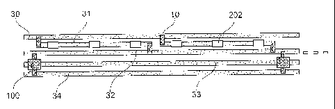
connected in such a manner that it may influence the lighting characteristics
of the LED
light wire. FIGURE 18 shows an embodiment of the integrally formed single
piece LED
light wire with sensors or detectors. As shown, there are four continuous
conductors
corresponding to conductive bus elements 30, 32, 33 and 34. Zero ohm jumpers
or
resistors 10 couple conductive segments 31 to conductive bus elements 30 and
32.
Conductor bus element 32 acts as a common ground. Conductive bus element 30
provides power to the LEDs 202, while conductive bus element 34 provides power
to
the sensor/detector 100. Conductive bus element 33 may direct the signal from
the
sensor/detector 100 to a power source which supplies power to the LEDs 202;
thereby,
allowing the sensor/detector 100 to influence the lighting characteristics
(e.g., intensity,
color, pattern, on/off) of the LEDs 202.
[00124] FIGURES 19A and 19B show a full color integrally formed single piece
LED
light wire having three continuous conductors corresponding to conductive bus
elements L1, L2 and L3 which supply power to the LEDs 202, and conductor
segments
S1 and S2 connecting the LEDs 202 to conductive bus elements L1, L2 and/or L3.
In
FIGURE 19B, the LEDs 202 are SMD-On-Board LEDs.
[00125] In another embodiment, each pixel of LEDs (or LED module) may be
controlled
independently. FIGURE 24 shows the configuration of an individually
controllable LED
light wire using seven conductors and LED modules 2120. Here, conductive bus
element 80 acts as a power ground, while conductive bus element 81 acts as a
voltage
in. Each LED module 2120 includes a microprocessor, at least one LED, power
input
and output connections, control signal input and output connections, and data
input and
output connections. In FIGURE 24, the LED modules 2120 include VCC pins, VDD
pins, enable pins, clock pins and data pins. The control signal and data input
connections of each LED module are coupled to the control signal and data
input
connections of an adjacent LED module. An optocoupler may be used to insulate
the
control signal line between each LED module. The LED modules 2120 may be
connected in series (for example, as shown in FIGURE 24) or in parallel (for
example,
the power input connections of each LED module 2120 is coupled to the first
conductive
22
CA 02741430 2011-04-21
WO 2010/081559 PCT/EP2009/050581
bus element 81 and the power output connection of each LED module 2120 is
coupled
to the second conductive bus element 80).
[00126]A plurality of integrally formed single piece LED light wires (such as
LED light
wire 12, 13, 14) may be aligned side-by-side to form a lighting panel 3000 as
shown in
FIGURES 25A-25C. Each LED light wire may contain an interlocking alignment
system
comprising an alignment key 60, 62 and an alignment keyhole 61, both of which
are
pre-formed in the encapsulant of the LED light wire, wherein the alignment key
60, 62
and the alignment keyhole 61 are located at opposite sides of the LED light
wire. The
alignment key 60, 62 and the alignment keyhole 61, 63 may continuously extend
or
intermittently extend longitudinally along the length of the LED light wire.
The alignment
keyhole 61, 63 may be in the form of a notch, a groove, a recess, a slot, or
an aperture,
and the alignment key 60, 62 may be in a form (including, but without
limitation, a rail or
a peg) which permits a friction fit (preferably, a snug fit) to the alignment
keyhole 61, 63.
The alignment key 60, 62 may have a width approximately equal to or slightly
larger
than the width of the alignment keyhole 61, 63, such that the alignment key
60, 62 may
fit therein in a friction fit, as shown in FIGURES 25B and 25C. As an example,
the
alignment keyhole 61, 63 may be a groove being adapted to friction fit with a
rail-shaped
alignment key 60, 62, both groove-shaped alignment keyhole 61, 63 and rail-
shaped
alignment 60 continuously extending longitudinally along the length of the LED
light
wire.
[00127]Although specific embodiments have been illustrated and described
herein, it
will be appreciated by those of ordinary skill in the art that a variety of
alternate and/or
equivalent implementations may be substituted for the specific embodiments
shown and
described without departing from the scope of the present invention. This
application is
intended to cover any adaptations or variations of the specific embodiments
discussed
herein. Therefore, it is intended that this invention be limited only by the
claims and the
equivalents thereof.
23