Note: Descriptions are shown in the official language in which they were submitted.
CA 02743117 2011-05-09
WO 2010/086773 PCT/IB2010/050293
METHOD FOR PATTERNING NANO-SCALE PATTERNS OF MOLECULES ON
A SURFACE OF A MATERIAL
BACKGROUND
[0001] The present invention relates to the field of probe-based methods for
patterning a surface of a material, such as scanning probe lithography (herein
after
SPL). In particular, embodiments are directed to high resolution patterning of
molecules on a surface of a material, such as nano-scale patterns with feature
sizes of
less than 30 nanometers (nm).
[0002] Lithography is a process for producing patterns of two dimensional
shapes, including drawing primitives such as lines and pixels within a layer
of
material, such as, for example, a resist coated on a semiconductor device.
Conventional photolithography (also called optical lithography) is running
into
problems as the feature size is reduced, e.g. below 65 nm. These problems
arise from
fundamental issues such as sources for the low wavelength of light, photoacid
migration, photoresist collapse, lens system quality for low wavelength light
and
masks cost. To overcome these issues, alternative approaches are required.
[0003] Examples of such alternative approaches are known in the field of the
so-called nano lithography, which can be seen as high resolution patterning of
molecules. Nanolithography refers to fabrication techniques of nanometer-scale
structures, including patterns having one dimension sizing up to about 100 nm
(hence
partly overlapping with photolithography). Beyond the conventional
photolithography, they further include such techniques as charged-particle
lithography (ion- or electron-beams), nanoimprint lithography and its
variants, and
SPL (for patterning at the deep nanometer-scale). SPL is for instance
described in
detail in Chemical Reviews, 1997, Volume 97 pages 1195 to 1230, 'Manometer-
scale
Surface Modification Using the Scanning Probe Microscope: Progress since
1991",
Nyffenegger et al. and the references cited therein.
CA 02743117 2011-05-09
WO 2010/086773 PCT/IB2010/050293
[0004] In general, SPL is used to describe lithographic methods wherein a
probe tip is moved across a surface to form a pattern. In other words,
scanning probe
lithography makes use of scanning probe microscopy (SPM) techniques, which
relies
on the availability of the scanning tunneling microscope. In short, it aims at
forming
images of sample surfaces using a physical probe. SPM techniques rely on
scanning
such a probe, e.g. a sharp tip, just above a sample surface whilst monitoring
interactions between the probe and the surface. An image of the sample surface
can
thereby be obtained. Typically, a raster scan of the sample is carried out and
the
probe-surface interaction is recorded as a function of position. Data are thus
typically
obtained as a two-dimensional grid of data points.
[0005] The resolution achieved varies with the underlying technique; atomic
resolution can be achieved in some cases. Use can be made of piezoelectric
actuators
to execute motions with precision and accuracy, at any desired length scale up
to
better than the atomic scale. The two main types of SPM are the scanning
tunneling
microscopy (STM) and the atomic force microscopy (AFM).
[0006] In particular, the AFM is a device in which the topography of a sample
is modified or sensed by a probe or probe mounted on the end of a cantilever.
As the
sample is scanned, interactions between the probe and the sample surface cause
pivotal deflection of the cantilever. The topography of the sample may thus be
determined by detecting this deflection of the probe. Yet, by controlling the
deflection of the cantilever and the physical properties of the probe, the
surface
topography may be modified to produce a pattern on the sample.
[0007] Following this idea, in a SPL device, a probe is raster scanned across
a
resist surface and brought to locally interact with the resist material. By
this
interaction, resist material is removed or changed. In this respect, one may
distinguish
amongst: constructive probe lithography, where patterning is carried out by
transferring chemical species to the surface; and destructive probe
lithography, which
includes physically and/or chemically deforming a substrate's surface by
providing
energy (mechanical, thermal, photonic, ionic, electronic, or X-rays energy,
etc.). SPL
is accordingly a suitable technique for nano lithography.
2
CA 02743117 2011-05-09
WO 2010/086773 PCT/IB2010/050293
[0008] High resolution patterning of molecules is relevant to several areas of
technology, such as alternatives to optical lithography, patterning for rapid
prototyping, direct functionalization of surfaces, mask production for optical
and
imprint lithography, and data storage.
[0009] In particular, lithography can be used for the fabrication of
microelectronic devices. In this case, electron-beam (or e-beam) and probe-
based
lithography are mostly in use.
[0010] For high resolution optical mask and nano-imprint master fabrication, e-
beam lithography is nowadays a standard technology. However, when approaching
high resolutions, writing times for e-beam mask/master fabrication increase
unfavorably.
[0011] As a possible alternative, the use of probes for such patterning is
still
under development. At high resolution (< 30 nm), the speed of single e-beam
and
single probe structuring converges.
[0012] In the case of data storage, various approaches have been proposed to
make use of probes for storage in the archival regime. However, a main
challenge that
remains is to achieve long bit-retention. Using thermomechanical indentation
allows
for instance to achieve satisfactory endurance and retention of data. A
thermomechanical approach, however, produces indentations that are inherently
under mechanical stress. Therefore it is difficult to obtain retention times
in excess of
ten years, as is usually desired in the archival domain.
3
CA 02743117 2011-05-09
WO 2010/086773 PCT/IB2010/050293
SUMMARY
[0013] In one embodiment, a probe-based method for patterning a surface of a
material is described. The method includes providing a material having a
polymer
film with a network of molecules cross-linked via intermolecular, non
essentially
covalent bonds. The method also includes patterning the polymer film by
desorbing
molecules from the network with a heated, nano-scale dimensioned probe.
[0014] In another embodiment, the method includes providing a material having
a polymer film with a network of molecular glass molecules. The molecules are
cross-linked essentially via hydrogen bonds. An average desorption energy of
the
molecules in the film is approximately between 2 eV and 3 eV. The method also
includes patterning the polymer film by desorbing molecules from the network
with a
heated, nano-scale dimensioned probe. The temperature of the probe is
approximately
between 300 C and 600 C. The time of exposure of the probe to the surface is
approximately between 0.3 microsecond and 10 microseconds. Other embodiments
of
the patterning method are also described.
[0015] Also, embodiments of a material are described. The material includes a
polymer film. The polymer film includes a network of molecules. The molecules
are
cross-linked via intermolecular, non essentially covalent bonds. The polymer
film
also includes nano-scale dimensioned patterns of molecules in the network.
Other
embodiments of the material are also described.
[0016] In another embodiment, a method of accessing (e.g., writing and/or
reading) patterns of molecules is described. The method includes providing a
material
such as the material described above. The method also includes accessing the
patterns
of molecules of the material. Accessing the patterns of molecules of material
includes
writing and/or reading the patterns of molecules. Other embodiments of the
accessing
method are also described.
[0017] Examples of methods and materials embodying aspects of the present
invention are described below, by way of non-limiting example, and in
reference to
the accompanying drawings.
4
CA 02743117 2011-05-09
WO 2010/086773 PCT/IB2010/050293
BRIEF DESCRIPTION OF THE DRAWINGS
[0018] FIGS. 1 - 3 schematically illustrate a process according to an
embodiment of the invention;
[0019] FIGS. 4 - 5 schematically depict another process according to another
embodiment;
[0020] FIGS. 6a - c show embodiments of schematized sections of nano-scale
dimensioned patterns in a patterned material;
[0021] FIG. 7 is an example of a molecular glass structure;
[0022] FIGS. 8 - 9 show cross sections of topographic images of surfaces
patterned according to the embodiment of FIGS. 1 - 3;
[0023] FIG. 10 is a cross section of a topographic image of a surface
patterned
according to the embodiment of FIGS. 4 - 5; and
[0024] FIG. 11 is a graph comparing cross-sections of a patterned material and
a pattern transfer into silicon.
5
CA 02743117 2011-05-09
WO 2010/086773 PCT/IB2010/050293
DETAILED DESCRIPTION
[0025] As an introduction to the following description, embodiments described
herein relate to a method for patterning a surface of a material. In one
embodiment, a
material having a polymer film thereon is provided. A probe is then used to
create
patterns on the film, by desorbing molecules at the surface thereof.
[0026] The film includes a network of molecules which are cross-linked via
intermolecular, noncovalent bonds, such as van der Waals forces, or hydrogen
bonds.
More specifically, such bonds are not of a covalent bonding nature (at least
not
essentially), that is, there is no clear electron pairing between radicals
that
characterizes the ordinary Heitler-London covalent bond. Rather, the
interaction
energy of the intermolecular bonds at stake could be divided into various
physically
meaningful components such as electrostatic, exchange, dispersion, relaxation,
etc.
Yet, none of the above components could be clearly called "covalent," inasmuch
as
anti-bonding mixing of atomic orbitals is likely to be involved, rather than
bonding
mixing. Should substantial charge-transfer be involved and be regarded as a
coordinate-covalent interaction, the occurrence of a substantial overlap
repulsion (i.e.,
the exchange component) would not make the molecules be viewed as covalently
bonded.
[0027] Rather, the intermolecular bonds provide a better comprise than the
usual chemical bonds, inasmuch as the film can remain stable under normal
conditions, less energy being yet required at the probe to create the
patterns.
[0028] In this regards, patterning the film is carried out by means of a nano-
scale dimensioned probe, which is further heated, such as to desorb molecules
when
interacting with (e.g., urged against) the film. In other words, molecules
evaporate
upon interaction with the probe. The probe thereby directly engraves patterns
into the
film.
[0029] Both the temperature of the probe and the time of exposure of the probe
to the surface can be adjusted according to a characteristic of the cross-
linked
molecules, in order to achieve desired desorption performances. The average
6
CA 02743117 2011-05-09
WO 2010/086773 PCT/IB2010/050293
desorption energy of the molecules can be seen as such a characteristic, which
is
impacted by the intermolecular bonds.
[0030] Since the binding energy caused by the intermolecular links is small
(at
least compared to covalent links), the process can work at moderate
temperatures and
short probe-sample interaction times. This, in turns, allows for scaling to
fast writing
times.
[0031] In reference to FIG. 1, a material is provided, having a polymer film
110
on a substrate 120. The film includes a network of molecules which are cross-
linked
via intermolecular bonds.
[0032] The probe 10 is an AFM probe mounted on the end of a cantilever, as
schematically represented in FIG. 1. At the apex thereof, the osculating
radius is
typically between 5 to 10 nm. More generally, dimensions of the probe are in
the
nanometer scale. The probe is part of an AFM device (not shown), comprising
electronic circuitry suitably designed to measure and control, in operation,
an
interaction between the probe 10 and a sample surface 111.
[0033] Engineering solutions may further be provided such that it is possible
to
accurately control the relative position of the probe and surface, and
possibly to
ensure good vibrational isolation of the AFM. This can, for instance, be
achieved
using sensitive piezoelectric positioning devices, as known in the art. Both
vertical 50
and horizontal 60 controls of the probe are thus typically provided together
with the
AFM.
[0034] In a usual AFM device, the probe 10 is likely to be raster scanned
above
the sample surface, such that imaging of the surface topology can be carried
out.
Here, the probe 10 will rather be used to engrave patterns on the surface 111,
as to be
explained in reference to FIGS. 1 - 5.
[0035] How the surface is patterned can be decomposed into several substeps.
First, the probe 10 is maintained in a "non-patterning position," that is,
close to the
surface 111 of the film 110 (step S 100, FIG. 1). The probe is not yet close
(or urged)
enough to enable surface patterning. More generally, conditions applied to the
probe
do, in a first substep, not allow for engraving a pattern.
7
CA 02743117 2011-05-09
WO 2010/086773 PCT/IB2010/050293
[0036] FIG. 2 is very similar to FIG. 1, except that the probe 10 is now urged
against the surface 111 of the film, and interacts therewith. The interaction
70 is
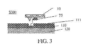
likely to desorb one or more molecules75, as illustrated in FIG. 3.
[0037] In some embodiments, the probe temperature (Tp) and the time (te) of
exposure of the probe to the surface are suitably adjusted, such as to change
or
optimize desorption of molecules. For example, the parameters may be adjusted
so as
to obtain regular patterns while minimizing the exposure time. Accordingly,
high
rates of primitive patterning can be achieved. In some embodiments, these are
close
to or even greater than one megahertz (MHz).
[0038] Incidentally, a person skilled in the art may appreciate in light of
the
subject matter described herein that, for a given load force, the above
parameters (Tp,
te) determine the desorption process, inasmuch as its rate constant roughly
obeys, in a
simple physical picture, the law r = Ae-E ikBT Here, A is the "attempt
frequency,"
that is, the chance of a molecule to overcome its potential barrier to
desorption, which
is partly determined by the exposure time. Furthermore, Ea is the activation
energy of
desorption of the cross-linked molecules, kB is Boltzmann's constant, and T is
the
temperature.
[0039] In addition, the skilled person may appreciate in light of the subject
matter described herein that the force applied to the probe while patterning
may
suitably be adapted in respect of the sample. Basically, in one embodiment,
both
temperature and force pulses are applied to the probe, at positions where the
molecules are to be removed. Quantitative details are provided below.
[0040] The desorption of a molecule 75 is depicted in FIG. 3. In some
embodiments, an assembly of molecules is likely to be desorbed by the probe,
during
a single exposure, that is, a single indent step, whereby pattern primitives
are
engraved. More specifically, the molecules are desorbed, that is, evaporated
by the
heated probe 10, instead of the film being thermomechanically indented or
locally
melted. Next, shortly before or after the molecule desorption, the probe is
released to
its non-patterning position, as in FIG. 1.
8
CA 02743117 2011-05-09
WO 2010/086773 PCT/IB2010/050293
[0041] The resulting material has nano-scale patterns of molecules on its
surface. By heating this material above a certain temperature, it is locally
evaporated,
as sketched in FIG. 6a. An advantage of using evaporation, in some
embodiments, is
that evaporated material is significantly and/or completely removed from the
sample
and not only pushed aside, in contrast to an elastic deformation were rims are
formed
at the edges of the pattern (as in FIG. 6b), or the density is locally
increased (FIG.
6c). The latter case is potentially disadvantageous when a subsequent etch
step is to
be contemplated.
[0042] Now, the patterns obtained so far are merely bidimensional inasmuch as
no information can be exploited from the depth of the pattern. Rather, a
gradient of
depth would be required to encode information. In this regards, the present
invention
can be embodied such as to create three-dimensional (3D) patterns of molecules
in
the film, as illustrated in FIGS. 4 - 5.
[0043] To this aim, one may first engrave a first pattern of molecules at a
given
location on the film, as represented in FIG. 4. Then, a second pattern can be
created
within the first pattern, as depicted in FIG. 5. In other words, repeated
exposures are
carried out. This amounts to engrave a pattern within an already existing
pattern.
Repeated exposures may achieve a pattern as depicted in FIG. 5, unless one or
more
parameters are varied during a single exposure. Incidentally, since such a
method is
maskless, there is comparatively little overhead associated therewith as
compared to
optical lithography, where several masks are fabricated and applied.
[0044] Alternatively, direct 3D-patterning in a single exposure step can be
attained by adjusting an evaporation volume at each location on the surface
that is
exposed. For example, one may contemplate modulating the force applied to the
probe during an exposure, e.g., using electrostatic actuations. Varying the
force
applied during an exposure results in a pattern with modulated depth.
Similarly, direct
3D-patterning can further be controlled by varying the temperature of exposure
(using
e.g. an integrated heater in the probe tip), or the exposure time.
[0045] Accordingly, a continuous change of topography can be carried out. This
way, 3D patterns can be obtained within a single exposure, i.e., a single
indent step.
9
CA 02743117 2011-05-09
WO 2010/086773 PCT/IB2010/050293
Depth modulated patterns are likely to allow for a dramatic improvement of a
writing
density. Incidentally, varying any of the above parameters (force,
temperature,
exposure time) or a combination thereof can already be contemplated for
creating 2D
patterns.
[0046] In addition, before the proper patterning steps, the depth of indents
may
be calibrated as a function of applied load and temperature, so as to set
specific and/or
optimal working conditions. For example, for a patterning depth of around 4
nm, a
temperature of 300 C and a load force of 80 nN may result to be optimal
(especially
for films as described below). Within such conditions, writing indents with a
pitch of
23 nm typically yields uniform removal of material over large areas. This
results in
patterned areas with distinct patterning depths, as discussed below with
reference to
FIGS 8 - 10. More generally, load forces of 50 - 100 nN may be convenient.
[0047] Furthermore, the ability to image the surface prior to patterning
enables
very accurate positioning. This becomes important notably when it comes to
patterning very fine features at high resolution over a pre-patterned surface
with
features that do not require such a high resolution (and which can be realized
using
more conventional patterning mechanisms with much higher throughput). Once the
pattern is written, it is possible to image it before further processing
steps. A post-
imaging allows for quality control of the written pattern and its eventual
correction.
[0048] At present, variants as to the types of suitable polymers are
discussed.
[0049] In one embodiment, the average molecular mass of molecules within the
film is less than about 4000 dalton (Da), in order to enable a desorption
process. Yet,
tests have shown that molecular masses in the approximate range from 100 Da to
2000 Da may make the process easier. More specifically, masses in the
approximate
range from 150 Da to 1000 Da may allow for increased and/or optimal
desorption, at
least for specific samples.
[0050] As described above, the molecules are cross-linked via e.g., hydrogen
bonds. A hydrogen bond is typically defined as the attractive force occurring
between
a hydrogen atom attached to an electronegative atom of a first molecule and an
electronegative atom of a second molecule. While its energy can be compared to
that
CA 02743117 2011-05-09
WO 2010/086773 PCT/IB2010/050293
of the weakest covalent bonds, the underlying physics cannot. Incidentally, a
typical
covalent (bonding) bond is about twenty times stronger than a typical hydrogen
bond.
Accordingly, relatively low desorption temperature and short interaction times
can be
contemplated in practice.
[0051] In one embodiment, the average desorption energy of the molecules is
approximately in the range from 2eV to 3eV, as the result of various
intermolecular
links in the media (including long-distance interactions). More generally,
desorption
energies approximately between 1 and 4 eV may be convenient.
[0052] Closely related, the temperature of the heated probe is approximately
between 300 C and 600 C. In some embodiments, it is approximately between 300
C
and 500 C, which may be optimal in some cases. As a side note, the temperature
of
the probe is believed to be about twice as much as the temperature of the
desorbing
molecules.
[0053] Meanwhile exposure times are typically in the range of 1 microsecond
( s) and 10 s. Yet, in some embodiments, it is possible to set the exposure
time to
about 0.3 s, with acceptable results. Roughly, exposure times of less than
about 1 s
allows for indent rates of 1 MHz.
[0054] Next, the network of molecules forming the film may include molecular
glasses. An example of a molecular glass molecule is represented in FIG. 7
(phenolic
compound). Such molecules include small molecules (with molecular masses
typically of about 1000 Da). These molecules do not properly crystallize due
to a
large number of configurations with merely equivalent conformational energy.
At the
periphery of the molecules, hydrogen bonding groups (Hydroxyl) establish the
physical links between the molecules.
[0055] The deposition of a thin film of this material onto a substrate (e.g.,
Si-
wafer) is simply done by spin-coating a solution of molecular glass, followed
by a
brief annealing step (e.g., about 1 minute at 130 C) to drive out the
solvent. No
further cross-linking reaction is required.
[0056] Due to the high number of hydrogen bonding interactions, the polymer
exhibits a relatively high glass transition temperature, Tg. In short, below
the
11
CA 02743117 2011-05-09
WO 2010/086773 PCT/IB2010/050293
temperature Tg, the structure of the polymer can be termed glassy, as it has a
merely
random arrangement of chains, similar to molecular arrangements seen in
glasses. In
some embodiments, Tg is of about 120 C, which is suited for use in patterning.
More
generally, the glass transition temperature is approximately between 80 C to
160 C,
and in some embodiments between 100 C and 130 C (e.g. 120 C), which may be
more suited for patterning in practice. Furthermore, hydrogen bonds make the
material stable against repeated scanning with the probe. It is accordingly
suitable for
use in the contexts of storage and lithography, for mask-repair and
inspection.
[0057] A proof of concept has been successfully performed by using a substrate
prepared as already mentioned. With typical writing conditions, patterns have
been
structured onto the polymer media. Specifically, the patterned surface at
stake is made
of a polymer of molecular glass molecules, cross-linked via hydrogen bonds. A
load
force of about 80nN was used to indent the patterns, together with a probe
temperature of nearly 400 C. The surface image was then obtained with the same
AFM probe as used to pattern.
[0058] FIGS 8 - 9 show typical experimental cross sections of topographic
images of the surface. Deflections d are in nm, while the x-coordinate is in
m. As
shown by the graphs, satisfactorily clean patterns are obtained, with vertical
resolution of about 1 nm or less. The depth of the patterned features is of
around 5
nm, as measured from the profiles. Here, it is possible to acknowledge the
approximately constant depth of the patterned features, and thus their
uniformity. The
second peak corresponds to a patterned feature having a width of about 30 nm.
Even
smaller features could actually be contemplated since the resolution in x is
currently
of 5 - 10 nm.
[0059] In FIG. 10, the cross section pertains to a sample surface patterned
according to a 3D patterning scheme as discussed above. Specifically, the
surface is
patterned by repeating exposures with same or similar conditions over an
already
exposed feature (i.e., a pattern). The features of the polymer film and
experimental
conditions used are otherwise the same as those leading to FIGS. 8 - 9. Again,
clean
3D patterns are obtained. The vertical resolution remains less than 1 nm.
12
CA 02743117 2011-05-09
WO 2010/086773 PCT/IB2010/050293
[0060] Next, it is pointed at the fact embodiments discussed above present
significant advantages in terms of pattern transfer. In this regards, pattern
transfer into
silicon can be performed by using standard dry-etching technique directly on a
patterned molecular glass that serves as the resist.
[0061] In an experimental test, the etch conditions used were 20 seconds in a
deep-reactive-ion etching tool, using a standard process gas mixture of 50%
SF6 and
50% C4F8. The resulting pattern in silicon reflected the topography of the
pattern in
the molecular glass. Yet, amplification of the pattern in the vertical axis
could be
controlled via the processing conditions. In particular, the pattern was
amplified five
times.
[0062] The results are illustrated in FIG. 11. The upper black curve pertains
to
the molecular glass surface. The lower grey curve relates to the etched Si
surface. As
can be appreciated, the quality of the transfer is satisfactory.
[0063] Lastly, a final experiment is briefly discussed. In this experiment, a
molecular organic glass is patterned. A thin film of 10-100 nm thickness is
prepared
by spin-coating or evaporation. By fine-tuning the inter-molecular
interaction, the
material can be desorbed by applying a thermomechanical trigger, i.e., a
probe,
leaving behind a well defined void. The probe tip temperature and the
mechanical
force are on the order of 300 - 500 C and 50 - 100 nN, respectively. By
laterally
displacing the probe and repeating the process, any arbitrary pattern can be
written,
the resolution of the process being determined by the apex dimensions of the
probe.
The patterns are written with a pitch of 29 nm, corresponding to 5x 10⁴
written marks,
resulting in uniformly recessed structures of 8 1 nm depth. The volume of
material
contained in the box amounts to 0.2 m3, yet no traces of material
displacement or
material redeposition are found. Similarly, no material pick-up by the probe
tip could
be detected by SEM after writing. Next, the structured glass could be used
without
any development step as a selective etch mask. Using a three layer technique
and
exploiting etch rate selectivities between organic materials and
silicon/silicon oxide,
it is possible to transfer the structure into silicon with excellent shape
conformity.
13
CA 02743117 2011-05-09
WO 2010/086773 PCT/IB2010/050293
[0064] In addition, material removal could be accumulated, thereby enabling
the fabrication of three-dimensional structures. As a test, a replica of the
Matterhorn
was accomplished by consecutive removal of molecular glass layers with defined
thickness. An almost perfect conformal reproduction of the original was
obtained,
proving that the final structure is a linear superposition of well defined
single
patterning steps. Moreover, results made it clear that the organic material is
neither
densified nor chemically altered during patterning.
[0065] The unique capabilities of embodiments of the technology recited above
open up new perspectives, notably for the fabrication of complex textured
substrates
for guided and directed assembly of shape-matching objects. The technique
further
offers a competitive alternative in terms of resolution and speed to known
techniques,
such as high-resolution electron beam lithography.
[0066] While the present invention has been described with reference to
certain
embodiments, it will be understood by those skilled in the art that various
changes
may be made and equivalents may be substituted without departing from the
scope of
the present invention. In addition, many modifications may be made to adapt a
particular situation to the teachings of the present invention without
departing from its
scope. Therefore, it is intended that the present invention not be limited to
the
particular embodiment disclosed, but that the present invention will include
all
embodiments falling within the scope of the appended claims. For example, the
present invention may be contemplated for various applications. While
embodiments
described above merely focus on uses for lithography and data storage, the
skilled
person may appreciate potential applications to pattern transfer of patterned
regions
into silicon.
14