Note: Descriptions are shown in the official language in which they were submitted.
CA 02743423 2011-05-11
WO 2010/059927 PCT/US2009/065300
VARIABLE PFC AND GRID-TIED BUS VOLTAGE CONTROL
Field of the Invention
This invention relates to the generation of compensation signals for power
converters
including but not limited to power factor correction (PFC) converters and grid-
tied inverters.
More specifically, the, present invention relates to methods of and
apparatuses for generating
a fast-loop response compensation signal that is substantially free of the
second harmonic AC
line-frequency ripple, typically 100 Hertz or 120Hz.
Background of the Invention
FIG. 5 is an exemplary prior art device for generating a compensation signal
for a
power converter. In the example shown, the compensation signal is for a power
factor
correction (PFC) converter. A PFC converter causes a power converter to appear
as a
resistive load to the network supplying power to the power converter. By
having the
conversion device appear as a resistive load, the power required from the
network versus the
power generated is optimized and thus the system is more efficient and draws
less current
than if the power converter presented a low-power-factor load to the network.
Prior art PFC
regulation loops generate a slow (typically 10Hz - 20Hz) compensation signal
for the PFC
converter to prevent compensation of second harmonic ripple (e.g. 100Hz or
120Hz) on the
output bus. Compensation of the second harmonic ripple reduces the power
factor of the PFC
converter, so prior art PFC regulation loops circumvent this problem by
slowing down the
compensation loop to the point of ignoring 100 Hz or 120 Hz ripple on the bus.
1
CA 02743423 2011-05-11
WO 2010/059927 PCT/US2009/065300
FIG. 5 illustrates a prior art circuit 500 for generating a compensation
signal 536 for a
PFC converter 540. A bus voltage 542 is provided to a voltage divider 520,
520' generating a
scaled-bus voltage 521. The scaled-bus voltage 521 is input into an inverting
input 531 of an
error amplifier 533. A reference voltage source 534 provides a reference
voltage to the non-
inverting input 532 of the error amplifier 533. The reference voltage source
534 is typically a
constant value scaled for a desired bus voltage 542. A filter compensation
network 535
response time of 100ms is typical to sufficiently remove the second harmonic
ripple from the
scaled-bus voltage 521 and produces an error reference signal 536 for the PFC
converter
controller 540.
Removal of a 100 Hz/120 Hz line ripple from the compensation signal 536 input
to
the PFC converter controller 540 prevents the PFC converter 541 from
responding to the
harmonic line ripple on the scaled-voltage bus 521. While the slow loop
response allows
filtering out of substantially all of the line-frequency ripple from the
reference bus signal, the
prior art design is not good at limiting transient voltage excursions caused
upon application of
a large load transient to a PFC converter 541. FIG. 6 illustrates various
waveforms for a
conventional prior art PFC converter system subject to a large load transient.
Waveform 6A
illustrates a curve of a load current as a function of time that incorporates
a step in output
load. The load current waveform 6A corresponds to a constant power load that
is stepped up
at time 400ms and stepped down at time 600ms. The ripple in the load current
is a direct
result of the variations in bus voltage and the fact that the load operates at
constant power.
Since PFC converters are usually connected to a second-stage converter which
is a DC-to-DC
converter, and the DC-to-DC converter acts as a constant power load, the
curves shown in
FIG. 6 correspond to a typical design situation.
2
CA 02743423 2011-05-11
WO 2010/059927 PCT/US2009/065300
The waveform 6B is a curve of AC input current into the conventional prior art
PFC
converter. The envelope of the AC input current rises between 400ms and around
450ms.
After removal of the AC load at 600ms, the AC input current drops back to pre-
load levels
after approximately 50ms.
The waveform 6C is a curve of the PFC output bus voltage coupled to a
conventional
prior art PFC converter. At time 400ms, at the application of the increased
load, the bus
voltage drops by about 50 volts between time 400ms and 430ms. This voltage
drop can
result in the undesirable side effect of causing the conventional prior art
PFC convertor to
drop out. The bus voltage recovers with some overshoot as shown around time
500ms. After
the increased bus load is removed (t=600ms), the bus-voltage overshoots by
around 30 volts
between the time of 600ms and 630ms. The bus voltage is shown recovering back
to the
previous value at about 700ms. Further, the negative-going voltage excursions
(Figure 6,
curve 6C, 400-460 ms) causes the second-stage converter to operate over a
larger voltage
range, thus reducing the holdup time of the power supply immediately following
a load
transient as well as increasing the converter cost and lowering the overall
converter
efficiency. To limit the effect of the large voltage transients, large
electrolytic capacitors are
placed on the output of the PFC stage resulting in an increase in the cost and
size for the PFC
converter.
The bus-voltage transients, resulting from the load transients can cause the
over-
voltage protection to temporarily shut down the power supply. Another result
of the
uncontrolled transients, due to the slow compensated error signal response (6D
in FIG. 6), is
for electronic devices requiring larger voltage operating ranges in the second-
stage converter
(power supply).
3
CA 02743423 2011-05-11
WO 2010/059927 PCT/US2009/065300
Waveform 6D illustrates a compensation signal (536 in Fig. 5) of a prior art
system
configured to generate a compensation signal for a PFC converter. Because of
the slow
response time of the compensated error signal 536, the PFC converter 540
cannot quickly
respond to the load transients (Figure 6, curve 6A), due to the need to not
respond to the line-
voltage second harmonic. The compensation signal is clearly shown in FIG. 6,
curve 6D.
The response time of about 60 ms is required to respond to the load transient.
As a result, prior-art PFC converter designs have a number of design
drawbacks.
First, higher voltage rated semiconductors are required because of the voltage
transients and
thus the PFC converter incurs a higher manufacturing cost. Second, the second-
stage
converter requires larger transformers to handle the higher voltage range and
thus impacts the
PFC converter with lower efficiency and higher cost. Additionally, hold-up
times following
load transients are reduced thus causing performance issues. System design
options are also
limited because unregulated converter stages cannot be used in tandem with a
PFC stage and
thus limiting potential increased performance and cost savings.
Grid-tied inverters are another example of power converters that must regulate
a DC
bus while ignoring voltage variations on the bus that contain the second
harmonic of the grid
frequency. Grid-tied inverters, such as some photovoltaic inverters, have the
same control
and compensation issue as PFC converters. FIG. 9 shows a schematic
representation of a
typical grid-tied inverter 900. The photovoltaic array 920 or other source of
power charges a
high-voltage bulk capacitor 940 through a DC-to-DC converter 910 at a constant
rate which
is dependent on the currently available power (e.g. as a function of the level
of light in the
case of a photovoltaic inverter). The full-bridge inverter formed by switches
(Q9 - Q 12)
951-954 and inductor (L6) 955 then produces a nearly sinusoidal current in
phase with the
4
CA 02743423 2011-05-11
WO 2010/059927 PCT/US2009/065300
grid voltage. As a result of the DC input power but sinusoidal output current,
the voltage
across bulk capacitor C3 contains a significant amount of second harmonic
(e.g. 100/120 Hz)
ripple. The inverter must adjust the amplitude of sinusoidal current that it
pushes into the
grid in order to regulate the voltage across bulk capacitor C3 940 to a
desired level. The
control loop to accomplish this regulation has exactly the same issues that
have already been
described for generating a PFC compensation signal.
What is needed is a circuit that produces a compensation signal representative
of the
bus voltage or that is substantially free of 100/120 Hz ripple but has a fast
response to
transients on the PFC converter (or grid-tied inverter) bus voltage.
Summary of the Invention
The present invention provides an apparatus for and method of generating a
compensation signal that is substantially free of power source AC line-
frequency harmonic
ripple. The compensation signal represents the deviation of the bus voltage
from a target
value that is substantially free of power source AC line-frequency harmonic
ripple, and can
be either a digital or analog signal. The error-signal provides a fast loop
response to the bus-
voltage transients. Although example embodiments are described herein
primarily with
digital processing of error-information, other implementations including
analog filters are
contemplated. Another implementation contemplated is a digital representation
of the filtered
bus information. This information can be scaled bus-voltage or error-voltage
information.
Further, a PLL can be implemented with analog or digital circuitry, the stack
containing bus
voltage data could be implemented with an analog charge coupled device, and
likewise the
compensation module filter can be implemented with analog circuitry.
CA 02743423 2011-05-11
WO 2010/059927 PCT/US2009/065300
One aspect of the invention is a device for generating a compensation signal
for a
power converter. The device is comprised of a frequency-locked system clock, a
bus-voltage
data generator, a stack of bus-voltage data, and a compensation module. The
frequency-
locked system clock has a frequency that is a multiple of an AC line-voltage
frequency. The
bus-voltage sampler provides bus-voltage data at the system clock frequency to
the stack
input. The bus-voltage data can be analog or digital and can represent bus-
voltage data or
error data representing the difference between the bus-voltage data and a
target bus voltage.
The stack has one or more outputs where voltage-bus data is output to the
compensation
module. The stack has a stack length which represents one or more complete
cycles of the
second harmonic of the AC line-frequency. The compensation module processes
data from
the stack forming a compensation signal output. The compensation signal is
formed to
minimize the frequencies at twice the power source AC line-frequency through
processing
stack data taken at a frequency, locked to the AC line-frequency, while
providing a fast
response to transients on the bus-voltage.
In one embodiment, the frequency-locked clock is a phase-locked-loop
configured to
selectively lock to twice the AC-line voltage frequency. The frequency-locked
clock can be
configured to only lock to frequencies between 64 Hz and 140 Hz.
In another embodiment the stack can have a digital or analog implementation.
The
analog stack comprises a charged coupled array that samples the bus-voltage
data. The
frequency-locked system clock is an analog device and the bus error data is
analog.
Comparing a scaled bus-voltage against a reference signal forms the analog bus-
error data.
The analog bus-error data is output to the stack.
6
CA 02743423 2011-05-11
WO 2010/059927 PCT/US2009/065300
In one embodiment, the compensation module comprises a means for summing the
bus-voltage data over one-half cycle of the AC-line voltage coupled to the
stack producing a
summer output, a scaled proportional component and a scaled integral component
coupled to
the summer output having a scaled proportional output and a scaled integral
output, a scaled
derivative component coupled to the stack and configured to process two bus-
voltage data
samples separated by one-half cycle of the AC-line voltage having a scaled
proportional
output, and a PID summer configured to sum the scaled proportional output, the
scaled
integral output, and the scaled derivative output, forming a compensation
signal. As with any
PID controller, not all of the P, the I, and the D signals are used in every
case. Different
combinations of the P, I, and D signal will provide different controller loop
responses. The
compensation signal can further comprise a scaled feed-forward component
having an input
coupled to the power converter bus, having a feed-forward output coupled to
the PID
summer, wherein the compensation signal further comprises a scaled feed-
forward signal
component. The compensation module can be embodied with digital components,
analog
components, or a combination thereof.
In a further embodiment, the device further comprises a converter module
having a
converter input configured to receive the compensation signal. The converter
module is
configured to convert the digital compensation signal to an analog
compensation signal on a
converter output. The converter output is configured to interface with a power
converter.
In another embodiment, the bus-voltage sampler can generate bus-voltage data
or
error data representing the differences between the bus-voltage value and a
target voltage
value. The data can be analog or digital.
7
CA 02743423 2011-05-11
WO 2010/059927 PCT/US2009/065300
In another embodiment, the device can be implemented in an ASIC (application
specific integrated circuit). Some of the larger filter components of the PLL
can be
implemented outside of the ASIC. Further, the ASIC can include the power
converter
controller as part of the device.
In another aspect of the invention discloses a method for generating a
compensation
signal for a power converter that is substantially free of AC power source
harmonics,
specifically the second harmonic. A method comprises the steps: generating a
frequency-
locked system clock having a frequency that is locked to an integral multiple
of an AC-line
voltage frequency, generating bus-voltage data at the frequency, queuing the
bus-voltage
data, and compensating the bus-voltage data thus forming a compensating signal
wherein the
compensation minimizes the compensation signal frequency components that are
at even
multiples of the AC-line voltage frequency. The frequency-locked system clock
is generated
at a multiple of the bus-voltage line frequency. The bus-voltage data can be
generated at a
scaled multiple of the system clock rate. The bus-voltage data is queued in a
stack at the
system clock rate. The stack output can be configured to output data in any
manner but
preferably is configured to output the most recent and the oldest bus-voltage
data. Preferably,
the stack length is selected to hold bus-voltage data representing one-half an
AC line cycle,
but the stack length can instead be selected to hold bus-voltage data
representing an integral
number of half-cycles. In another step, the method includes compensating the
bus-voltage
data and forming a compensation signal.
In one embodiment, the method of generating a frequency-locked clock is a
phase-
locked-loop configured to selectively lock to twice the AC-line voltage
frequency. The
8
CA 02743423 2011-05-11
WO 2010/059927 PCT/US2009/065300
method of generating a frequency-locked clock can be configured to only lock
to frequencies
within 64 Hz to 140 Hz.
In another embodiment the queuing can be digital or analog. The queuing can be
implemented with a stack comprised of a charged coupled array that samples the
bus-voltage
data. Further, generating the voltage-bus data can be analog or digital and
either provides
sample data or error data.
In one embodiment, the compensating includes a compensation module comprising
a
means for summing the bus-voltage data over one-half cycle of the AC-line
voltage
frequency coupled to the stack producing a summer output, a scaled
proportional component
and a scaled integral component coupled to the summer output having a scaled
proportional
output and a scaled integral output, a scaled derivative component coupled to
the stack and
configured to process two bus-voltage data samples separated by one-half cycle
of the AC-
line voltage having a scaled proportional output, and a PID summer configured
to sum the
scaled proportional output, the scaled integral output, and the scaled
derivative output,
forming a compensation signal. As with any PID controller, not all of the P,
the I, and the D
signals are used in every case. The compensation signal can further comprise a
scaled feed-
forward component having an input coupled to the power converter bus, having a
feed-
forward output coupled to the PID summer, wherein the compensation signal
further
comprises a scaled feed-forward signal component. The compensation module can
be
embodied with digital components or with analog components.
In a further embodiment, the device further comprises a converter module
having a
converter input configured to receive the compensation signal. The converter
module is
configured to convert the digital compensation signal to an analog
compensation signal on a
9
CA 02743423 2011-05-11
WO 2010/059927 PCT/US2009/065300
converter output. The converter output is configured to interface with a power
converter
controller.
In another embodiment, the generating bus-voltage data can generate bus-
voltage data
or error data representing the differences between the bus-voltage value and a
target voltage
value. The data can be analog or digital.
In one embodiment, some, all, or a combination of the steps can be performed
with
analog components and techniques. The frequency-locked system clock can be
analog and
the bus-error data can be analog. The stack of bus-error data can be an analog
charge coupled
device where the delay line length is one or more cycles of the bus-voltage
ripple. The
analog filtering can form a scaled derivative component and a scaled
proportional component
of the bus-error data as components of the target-voltage compensation signal.
In a further
embodiment, the filter includes a scaled integral component of the bus-error
data as part of
the target-voltage compensation signal. In a further embodiment, a scaled feed-
forward
component is added to the target-voltage compensation signal.
A third aspect of an invention discloses method of manufacturing a device for
generating a compensation signal for a power converter. The method comprises
the steps of
providing a frequency-locked clock coupled to an AC-line having an AC-line
voltage
frequency, wherein the clock is configured to generate a frequency that is
frequency locked to
an integral multiple of the AC-line voltage frequency, providing a bus-voltage
sampler
coupled to the frequency-locked clock and coupled to a power converter bus
having a bus-
voltage and generating bus-voltage data at the frequency, providing a stack
coupled to the
bus-voltage sampler, wherein the stack is sized to contain bus data-samples
spanning a time
interval of one-half cycle of the AC-line voltage, and providing a
compensation module,
CA 02743423 2011-05-11
WO 2010/059927 PCT/US2009/065300
operatively coupled to the stack, and configured to generate from the bus-
voltage data a
compensation signal, and wherein the compensation signal module is configured
to produce
a compensation signal in which the frequency components at even multiples of
AC-line
voltage frequency are minimized.
In one embodiment, the provided frequency-locked clock is a phase-locked-loop
configured to selectively lock to twice the AC-line voltage frequency. The
provided
frequency-locked clock can be configured to only lock to frequencies within 64
Hz to 140
Hz.
In another embodiment, providing the stack can be with digital or analog
components.
The stack can be an implemented with a charged coupled array that samples the
bus-voltage
data. Further, the generating the voltage-bus data can be analog or digital
and either provide
sample data or error data.
In one embodiment, the providing the compensating module comprises a means for
summing the bus-voltage data over one-half cycle of the AC-line voltage
coupled to the stack
producing a summer output, a scaled proportional component and a scaled
integral
component coupled to the summer output having a scaled proportional output and
a scaled
integral output, a scaled derivative component coupled to the stack and
configured to process
two bus-voltage data samples separated by one-half cycle of the AC-line
voltage having a
scaled proportional output, and a PID summer configured to sum the scaled
proportional
output, the scaled integral output, and the scaled derivative output, forming
a compensation
signal. As with any PID controller, not all of the P, the I, and the D signals
are used in every
case. The compensation signal can further comprise a scaled feed-forward
component having
an input coupled to the power converter bus, having a feed-forward output
coupled to the PID
11
CA 02743423 2011-05-11
WO 2010/059927 PCT/US2009/065300
summer, wherein the compensation signal further comprises a scaled feed-
forward signal
component. The compensation module can be embodied with digital components or
with
analog components.
In a further embodiment, the method further comprises providing a converter
module
having a converter input configured to receive the compensation signal. The
converter
module is configured to convert the digital compensation signal to an analog
compensation
signal on a converter output. The converter output is configured to interface
with a power
converter.
In another embodiment, the providing a bus-voltage sampler data can generate
bus-
voltage data or error data representing the differences between the bus-
voltage value and a
target voltage value. The data can be analog or digital.
In one embodiment, some, all, or a combination of the steps can be performed
with
analog components and techniques. The frequency-locked system clock can be
analog and
the bus-error data can be analog. The stack of bus-error data can be an analog
charge coupled
array where the delay line length is one or more cycles of the bus-voltage
ripple. The analog
filtering can form a scaled derivative component and a scaled proportional
component of the
bus-error data as components of the target-voltage compensation signal. In a
further
embodiment, the filter includes a scaled integral component of the bus-error
data as part of
the target-voltage compensations signal. In a further embodiment, a scaled
feed-forward
component is added to the target-voltage compensation signal.
These and other aspects, features and advantages of the invention are
understood with
reference to the drawing figures and detailed description herein, and are
realized by means of
the various elements and combinations particularly pointed out in the appended
claims. It is
12
CA 02743423 2011-05-11
WO 2010/059927 PCT/US2009/065300
understood that both the foregoing general description and the following brief
description of
the drawings and detailed description of the invention are exemplary and
explanatory of
preferred embodiments of the invention, and are not restrictive of the
invention, as claimed.
13
CA 02743423 2011-05-11
WO 2010/059927 PCT/US2009/065300
Brief Description of the Drawings
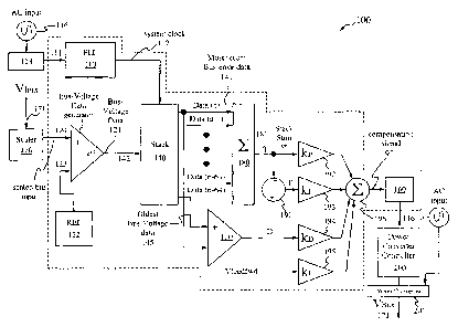
FIG. 1 illustrates a block diagram of a circuit for generating a fast loop
response
compensation signal for a power converter that is substantially free of second
harmonic AC
line-frequency ripple, according to one embodiment of the invention.
FIG. 2 illustrates one embodiment of the block diagram of the PLL of FIG. 1.
FIG. 3 illustrates the method to generate a compensation signal substantially
free of
second harmonic AC-line frequency ripple from a power converter bus voltage
having a
second harmonic AC line-frequency ripple.
FIG. 4 illustrates the method to manufacture an apparatus to generate a fast
loop
response compensation signal for a power converter bus that is substantially
free of second
harmonic line-frequency ripple.
FIG. 5 illustrates the prior art for generating a slow response compensation
signal for
a power converter.
FIG. 6 shows graphs of the bus-voltage, input current, and compensation signal
in
response to transient load changes for a prior art system.
FIG. 7 shows graphs of the bus-voltage, input current, and compensation signal
in
response to transient load changes for a system with a fast-loop response
compensation
signal.
FIG. 8 shows graphs illustrating the differences in signals between a standard
PID
Titer and a modified PID' filter in response to an input change.
FIG. 9 illustrates a block diagram of a prior-art photovoltaic grid-tied
inverter.
14
CA 02743423 2011-05-11
WO 2010/059927 PCT/US2009/065300
Detailed Description of the Present Invention
Certain embodiments of the present invention are directed to an apparatus and
method
for generating a fast-loop compensation signal for a power converter,
including but not
limited to a PFC converter or grid-tied inverter. The compensation signal is
designed to have
a fast response to changes in the power converter's load but not respond to
the second
harmonic of the AC power source frequency, typically 100/120 Hz. The following
description of the invention is provided as an enabling teaching of the
invention that includes
its best, currently known embodiment. One skilled in the relevant art will
recognize that
many changes can be made to the embodiment described, while still obtaining
the beneficial
results of the present invention. It will also be apparent that some of the
desired benefits of
the present invention can be obtained by selecting some of the features of the
present
invention without utilizing other features. Accordingly, those who work in the
art will
recognize that many modifications and adaptations to the present inventions
are possible and
may even be desirable in certain circumstances, and are a part of the present
invention. Thus,
the following description is provided as illustrative of the principles of the
present invention
and not in limitation thereof, since the scope of the present invention is
defined by the claims.
The following description uses a generic power converter for illustration;
however, all
of the principles described apply equally to generating a compensation signal
for but not
limited to a PFC converter or a grid-tied inverter.
In the preferred embodiment of the invention, a PLL provides a frequency-
locked
clock to the second harmonic of the power converter's AC power source,
typically 100 Hz or
120 Hz. The PLL provides a clock that is frequency-locked to the rectified AC
power source
line-frequency or at an integral multiple of the AC power source line-
frequency. The
CA 02743423 2011-05-11
WO 2010/059927 PCT/US2009/065300
frequency-locked clock, or an integral multiple or integral fraction, or
combination thereof of
the frequency-locked system clock is distributed to other circuit modules. A
bus-voltage
sampler provides information about the bus-voltage. Preferably, the bus-
voltage sampler
provides bus-voltage data representing error values proportional to the
difference between the
bus voltage value and a target value; however, bus-voltage data can instead
represent samples
of the bus-voltage values rather than error values. The stack contains bus-
voltage data which
has been sampled over a period equal to an integral multiple of one half of
the AC-line cycle.
The PID' signal is generated by summing three values either through analog or
digital
methods. The modified proportional (P') signal is a scaled value of the stack
sum. The
modified integral (I') signal is an integrated value of the stack sum scaled
by a second value.
The modified derivative (D') signal is the difference between the oldest stack
bus-voltage
error data and the current bus-voltage data scaled by a third value. The three
scaling values
are chosen to produce a fast but stable compensation loop based on techniques
commonly
practiced by those skilled in the art of power supply design. The P', the I',
and the D' signals
are substantially free of second-harmonic line frequency content. The P'
signal was already
shown to contain no second-harmonic line frequency content because the stack
contains
equally spaced bus-voltage data representing exactly one line-frequency half-
cycle due to the
frequency locked clock. The I' signal is an integral of the P' signal, so it
too is substantially
free any second-harmonic line frequency content. The D' signal is the
difference between
two samples (oldest stack sample and current error) which are spaced apart in
time by exactly
one-half line cycle. In the case of steady-state converter operation, the
oldest and newest
bus-voltage error data are identical so the D' signal is zero, thus
substantially free of second-
harmonic line frequency content. The resulting PID' controller therefore
ignores 100/120 Hz
16
CA 02743423 2011-05-11
WO 2010/059927 PCT/US2009/065300
harmonics but responds in a controlled manner to transients on the bus
voltage. The digital
PID' target-voltage compensation signal can be directly coupled to a digital
input on a
digitally implemented PFC converter control, or can be converted into an
analog signal and
used with an analog PFC converter control.
FIG. I illustrates a block diagram 100 of one embodiment of a system for
generating a
fast loop response compensation signal 197 for a power converter controller
200. The system
comprises a second-harmonic line frequency detector 113, a phase-locked loop
(PLL) 110, a
bus-voltage sampler or data generator 120, a stack 140, a modified derivative
data D'
generator 130, a voltage scaler 170, a summer 180, a proportional data scaler
192, an
integrator 191, and integrator data scaler 193, a derivative scaler 194, a
feed-forward scaler
195, a compensation signal component sun-uner 196, and an optional signal
converter 160.
The second-harmonic line frequency detector 113 can be any means known in the
art
to produce a strong signal component at twice the frequency of the AC line
input. In
practice, the second-harmonic line frequency detector 113 will typically be
created by
comparing a full-wave rectified AC line voltage to a fixed reference level;
however, there are
many other methods to produce pulses at a frequency equal to the second-
harmonic of the
input line frequency. The PLL 110 is one means for producing a frequency-
locked clock but
other means are contemplated. The PLL 110 locks to the second harmonic of the
AC-line
frequency, typically at 100 Hz or 120 Hz, and generates a phase-locked system
clock 112
which is a multiple of the second-harmonic line frequency. The frequency
multiplication is
accomplished by placing a frequency divider in the feedback path of the PLL
110. So, for
example, if the frequency divider divides the frequency by a factor of 64 and
the AC line
frequency is 50Hz, then the second-harmonic line frequency detector will
produces pulses at
17
CA 02743423 2011-05-11
WO 2010/059927 PCT/US2009/065300
a rate of 100Hz and the PLL 110 will produce a frequency-locked system clock
at a
frequency of 6.4kHz. One could obtain the same result by having the PLL 110
lock to the
AC line frequency (rather than the second harmonic of the line frequency) and
then multiply
the input frequency by an additional factor of two. The PLL 1 10 can be
analog, digital, or a
combination of both. Integrated ASIC version of a PLL 110 can be used. Some of
the analog
filter components can be too large to economically implement in an ASIC and
thus kept
external from a PLL ASIC design.
The frequency-locked system clock output 112 is coupled to the system
components
that require synchronization with the frequency-locked system clock which
includes the stack
140, and in practice will also include all elements of the system which are
implemented
digitally.
The voltage scaler 170, typically a voltage divider composed of resistors,
scales the
bus voltage 171 to produce scaled bus input 124 which is input into a bus-
voltage data
generator 120. The purpose of the scaler 170 is to lower the bus-voltage data
samples to a
level compatible with the other electronics. The bus voltage 171 can be
hundreds of volts.
The bus-voltage sampler 120 can generate data in a number of different forms.
The
bus-voltage data output 121 can be digital or analog. Further, the bus-voltage
data can
represent a scaled bus-voltage or a scaled error value from a target voltage.
As shown in
FIG. 1, an error signal is generated representing the difference between a
scaled bus voltage
124 and a reference signal generator 122. A reference voltage 122 is coupled
to the
alternative input 123 into bus-voltage sampler 120. The reference voltage 123
and the scaled
bus voltage 124 are selected such that the difference, i.e. the error, is zero
when the bus
voltage 171 is at a target level. In operation, the bus voltage and thus the
scaled-bus voltage
18
CA 02743423 2011-05-11
WO 2010/059927 PCT/US2009/065300
input 124 has 100/120Hz ripple on the signal and thus the difference between
the reference
voltage 122 and the scaled bus voltage 124 will reflect this ripple. In a
configuration where
bus-voltage samples are generated, instead of error bus-voltage samples, then
other
electronics in the summer 180, stack 140, or in other electronics (not shown)
can subtract out
the DC bias in the data; however, it is advantageous to use error samples
rather than bus-
voltage samples in order to reduce the required dynamic range of the
computational
hardware. It is apparent to one skilled in the art that by changing the
reference voltage 122,
or the scaling factor in the voltage scaler 170, that different target bus
voltages 171 can be
selected. A typical value for voltage reference 122 is approximately 2.5 volts
or 1.25 volts.
The bus-voltage sampler 120 provides bus-voltage data 121 to the stack 140.
The bus-voltage data 121 is input into the stack 140 on the input 142. A
frequency
locked system-clock 112 is provided to the stack 140 from the PLL 110 to
control the rate
and location at which bus-voltage data is input, output, and stored in the
stack 140. The stack
140 is sized to hold samples representing a time interval of one-half cycle of
an AC-line
voltage. Multiples of this stack size are also contemplated by this
disclosure. Preferably, the
stack is digital and receives digital bus-voltage data but an analog
implementation is also
contemplated. An analog version of the stack 140 can be implemented with chain
of charged
coupled devices called a charge coupled array. Samples of bus-voltage data are
stored as
voltage charges within the charged coupled array.
The summer 180 averages the bus-voltage data 121 from the stack 140 over one-
half
cycle of the AC-line equivalent to one cycle of the second harmonic of the AC-
line. Because
the bus-voltage data 121 is frequency locked to the second harmonic of the AC-
line
frequency, the sum of the second harmonic components will average
substantially to zero
19
CA 02743423 2011-05-11
WO 2010/059927 PCT/US2009/065300
when the converter has a constant load. Noise and resolution limitations will
typically
provide some residual data at the second harmonic. The sum 180 can be
calculated by either
an analog means or a digital means. If the bus-voltage data 121 does not
represent error
values, then preferably DC offset is subtracted from each bus-voltage data 121
sample.
Preferable, the sum is calculated by keeping a running sum of the samples by
subtracting the
oldest sample and adding the newest sample.
In the embodiment shown, the stack 140 provides an output for the latest
value,
Error(n), and the error value Error(n-64) delayed by one-half cycle of the AC
line or a full
cycle of the AC-line second harmonic. The derivative generator 130 generates a
difference
value D' which can be analog or digital. The bus-voltage data samples on the
oldest bus-
voltage data output 145 are delayed by the stack length that is shown as 64
bus-voltage data
samples. The stack length is sized to cover a half-cycle of the AC line or a
full cycle of the
AC-line second-harmonic ripple. Thus, by choosing a stack depth that is locked
to the time
of one cycle of the second harmonic ripple, the differential signal component
D' is free of the
AC second harmonic. This illustrates a relationship between the system clock
112 and the
stack depth. A doubling of the system clock 112 will require a doubling of the
stack depth.
An implementation of a compensation signal generator utilizing a modified PID'
filter
is illustrated in FIG. 1. The embodiment shown comprises a modified PID'
(proportional,
integral, derivative) filter and can optionally include a feed-forward signal.
The feed-forward
signal is coupled to the bus voltage 171. The system disclosed generates a
compensation
signal that differs from prior art compensation signals. The modified PID'
filter utilizes AC-
line frequency-locked bus-voltage data which provides the advantage of being
able to remove
the AC-line second harmonic from the generated compensation signal 197. A half-
cycle sum
CA 02743423 2011-05-11
WO 2010/059927 PCT/US2009/065300
180 of the bus-voltage data 121 is generated and used to generate a modified
proportional
signal P', from which a modified integral signal Pis generated. The summer 180
can be
generated by any standard means including but not limited to inputting from
the stack 140 the
entire AC-line half-cycle of stack bus-voltage data 121 or by computing a
running sum by
subtracting the oldest stack value (Data(n-64)) which is being "pushed" out of
the stack and
adding the newest stack value (Data(n)). The modified P' value is used by the
modified
integrator 191 to generate the modified I' compensation signal component. A
modified
derivative value D' is generated by inputting the current bus-voltage data
(Data(n)) and the
half-cycle delayed bus-voltage data (Data(n-64)) into a differential generator
130 which
outputs D'. The differential generator 130 can be analog or digital. The P
data is scaled by
Kp 192, the I' data is scaled by K1193, and the D' data is scaled by KD 194.
The scaled P', I',
and D' values are input into a summing device 196 producing a composite
compensation
signal 197. One skilled in the art of power controller design is able to
determine the scaling
values of Kp 192, K1193, KD 194 to provide a desired response of the PID'
filter.
Additionally, the compensation signal can include a feed-forward signal
Vfaodfwd scaled by KF
195. The scaled feed-forward signal can also be input into the summer 196
forming a
component of the compensation signal 197. The compensation signal 197 can be
input into
an optional converter 160 that converts the compensation signal into a signal
compatible with
a power converter controller 200. The converter 160 can convert a digital
target bus-voltage
compensation signal into an analog signal. The compensation signal 197
provides a scaled
fast response control signal for the power converter controller 200 that
responds to a change
in the bus voltage 171. Furthermore, the compensation signal 197 is
substantially free of AC
21
CA 02743423 2011-05-11
WO 2010/059927 PCT/US2009/065300
100/120 Hz line-ripple and accordingly, the power converter 201 bus voltage
has better
transient response characteristics by not responding to this ripple.
The dashed line within the block diagram represents the components that are
preferably implemented in a single integrated circuit such as an ASIC
(application specific
integrated circuit). The filter components of the PLL typically are not
included in an ASIC
because of the components size.
FIG. 2 illustrates a block diagram of the PLL 110 of FIG. I including the
filter
components. The PLL clock generation circuit comprises a phase detector 114,
notch filter
components 115, a notch filter 116, a VCO (voltage controlled oscillator) 117,
and clock
divider 118. The input to the PLL circuit 110 is a second harmonic input at
twice the AC-line
frequency. The phase detector 114 generates an output signal based on the
phase differences
between the second harmonic pulses 113 and the output of the frequency divider
118. The
output of the phase detector 114 is input into a notch filter 116 with a pass-
band between 64
Hz and 140 Hz. The filter components 115 are coupled to the notch filter 116.
The output of
the notch filter 116 is coupled to a VCO 117. The output of the VCO 117 is a
frequency-
locked system clock 112. The frequency-locked system clock output 112 is
coupled to the
frequency divider 118. The dashed line represents the components that can be
formed within
the single integrated circuit.
In the present illustration, the VCO has a frequency that is 64 times the
output from the
second-harmonic generator, or 128 times the AC-line frequency. The frequency
divider 118
divides the VCO 117 clock frequency down to a frequency equal to the output
from the
second-harmonic generator. The notch filter 116 constrains the PLL 110 to only
respond
over a narrow frequency band corresponding to the expected range of AC line
frequency.
22
CA 02743423 2011-05-11
WO 2010/059927 PCT/US2009/065300
In operation, the PLL 110 shifts the VCO clock frequency so that the system
clock
112 is frequency locked with the AC line-frequency and thus is frequency
locked with the
ripple components on the bus voltage 171. The PLL 110 provides a system clock
output 112.
Fig. 8 illustrates the difference in signals between a true PID (proportional,
integral,
derivative) controller and the signals generated by the present invention PID'
controller for an
input ac line at 50Hz. Waveform 8E (Vbus) in FIG. 8E shows a bus voltage
experiencing a
positive and negative step. From left to right: Vbus starts at 385V. At
t=400ms, Vbus rises
to 425V in Ims. Vbus then remains at 425V until t=501ms. At t=501ms, Vbus
decreases to
385V in lms. The Vbus excursions do not represent any particular closed-loop
converter
operation. To illustrate the difference between a PID and a PID' signal, 100Hz
ripple is not
included on the Vbus signal in FIG. 8E. If one uses a true PID controller on a
ripple free bus,
then the proportional signal P follows the waveform of Vbus. Note, in waveform
8D that P'
lags behind P because the entire register stack requires filling with the
higher-voltage values
of Vbus in order for the stack average to have equivalence to the true
proportional signal P,
and it takes l Dins (a half-cycle for a converter operating at 50Hz) for the
register stack to fill
with error signals corresponding to the new Vbus value. The stack and summer,
driven by a
frequency locked clock, are required to remove the second harmonic ripple and
thus provide
a modified response PID' filter. The stair step transient response of P' is a
result of discrete
changes to the register stack values.
The waveform 8A shows at time 400ms the derivative response "D" to a step wise
increase in the bus voltage and at about time 500ms the step decrease in bus
voltage.
Waveform 8B shows the effect on D', the modified derivative response signal,
to a step
increase in bus voltage of the present invention. The derivative signals D and
D' have similar
23
CA 02743423 2011-05-11
WO 2010/059927 PCT/US2009/065300
fast responses to the onset of the transients; however, whereas D decreases to
0 volts
immediately corresponding to the end of the Vbus transient, D' does not
decrease to zero until
l Orris (a half-cycle for a converter operating at 50Hz) following the onset
of the transient.
The waveform 8C shows the modified integral signal I' The modified integral
signal I'
is similar to the true integral signal I with a slight delay of about 4ms. The
delay is caused by
a difference between the area under P and the area under P at the transients.
One can see that the modified PID' signals depart from the true PID signals;
however,
one can also see that the transient information shows up in P', I', and D'
immediately
following the onset of the transient. In practice, one can make a PID'
controller using the
modified signals P', I', and D'. The response using the modified control
signals is different
from that of a control implemented with true PID signals, but the results are
adequate to
implement a fast responding and stable control with the modified signals.
Figure 7 illustrates the benefits of a power converter utilizing a
compensation signal
generated from the voltage bus data that has had the second harmonic ripple
removed in the
generation of a compensation signal. The waveform 7A shows a step increase in
the load.
The load increase occurs at time 400ms and decreases at 600ms. Waveform 7B
shows the
corresponding AC current draw. As expected, the AC current draw increases
between 400ms
and 600ms to meet the increased load. There is a slight overshoot in the
current draw as the
converter quickly responds to the transient. Waveform 7C shows the bus voltage
out of the
power converter with a target bus-voltage compensation signal of the present
invention. Note
the small change in the bus voltage as compared to the prior-art of FIG. 6.
The bus voltage
deviates from its steady-state value by only about 2V, compared to a 50V
deviation seen in
the prior-art waveform 6C of FIG. 6. The waveform 7D represents the
compensation signal
24
CA 02743423 2011-05-11
WO 2010/059927 PCT/US2009/065300
waveform generated by the present invention. One can see that the compensation
waveform
shows a very fast response to the transient, as compared with the prior-art
waveform 6D of
FIG. 6.
FIG. 3 illustrates a flow chart 300 of the method of generating a compensation
signal,
either digital or analog, for a power converter where the compensation signal
is substantially
free of the 100/120 Hz line-frequency ripple. In the step 310, a frequency-
locked system
clock is generated that is phased locked to an AC line-frequency. The system
clock can be
generated by a number of means including a PLL comprising analog components,
digital
components, or a combination thereof. The AC line frequency, to which the PLL
locks, can
be designed to only lock to frequencies of between 64 Hz to 140.Hz. Limiting
the frequency
range to which the PLL will lock reduces the possibility of accidental locking
to a frequency
other than the 100/120 Hz second harmonic AC line-frequency ripple. The
frequency-locked
system clock is provided to the rest of the system for synchronous bus-voltage
data
generation, queuing the data, and forming the compensation signal. The
generation of the
frequency-locked system clock can be implemented with discrete components or
can be an
integrated component. Further, the frequency-locked system clock can be part
of a larger
system integrated circuit.
In the step 320, bus-voltage data is generated at a frequency-locked system
clock rate.
Digital samples can be generated by an A/D (analog-to-digital) converter and
can be
buffered. Any A/D converter can be used for generating bus-voltage data so
long as the
converter can take samples at the desired system clock rate. The resolution
(number of bits)
of the samples can be selected to provide sufficient sensitivity to process
the AC line ripple
that is riding on top of the bus voltage. The fewer bits of resolution the A/D
has, the more
CA 02743423 2011-05-11
WO 2010/059927 PCT/US2009/065300
quantization noise in the bus samples and the less sensitivity in generating a
control signal
that does not contain AC ripple components. Further, the larger the bus
voltage, the greater
the range needed by the A/D. An A/D with 12-bits of resolution provides a 400V
bus with
approximately 100 mV resolution, but provides a bus-voltage of 80V with
approximately
20mV resolution. A 10-bit A/D provides substantially the same resolution for a
system with
a 100V bus voltage or 20V error range. Thus, the number of bits of resolution
on the A/D
can be selected to match the minimum desired level AC-ripple on the control
signal. The
buffered samples are output for queuing. If bus-voltage data is queued in an
analog form,
then the bus-voltage data can be level shifted, scaled, and buffered before
being input into the
stack.
In the step 330, the bus-voltage data is stored in a stack. Preferably, the
stack
provides a way to output data delayed by the stack size and also provide an
output for the
latest sample value. However, other stack configurations can be used. Bus-
voltage data is
moved into the stack and output from the stack at a frequency-locked system
clock rate. The
stack is sized to provide a bus-voltage data delay of one-half cycle of the AC
line between the
last entered bus-voltage data value and the oldest bus-voltage data value. The
stack size is
equivalent to one cycle of the rectified bus input signal. A convenient stack
depth is sixty-
four samples but other stack sizes are within the scope of the invention.
Preferable, the stack
is implemented with digital technology known by one skilled in the art of
digital components.
Also, an analog version of the stack is contemplated. Charge coupled devices
can be used to
store analog bus-voltage data samples.
In the step 340 a compensation signal is generated from bus-voltage data that
is
substantially free from second harmonic ripple from the AC-input voltage. The
ripple free
26
CA 02743423 2011-05-11
WO 2010/059927 PCT/US2009/065300
data for a proportional compensation signal component and an integral signal
component is
generated by a summer that keeps a running sum of the stack values. Because
the data in the
stack is frequency locked with the AC-line voltage ripple and represents
exactly one cycle of
the second harmonic AC line ripple, the sum of the stack values will sum to
zero.
Accordingly the proportional and integral compensation signal generation
components are
free from second AC-line voltage harmonics. The differential compensation
signal
component is generated from bus-voltage data that is separated in time by one
cycle of the
second harmonic of the AC-line voltage. Accordingly, this differential
component is free of
second harmonic ripple. These three components, each scaled, form a modified
PID'
(proportional, integral, differential) compensation signal. The compensation
signal generator
can be analog or digital. Preferably the signal is digital.
In the optional step 350, the compensation signal is converted to a format
compatible
with the power converter controller (200-FIG. 1). If the compensation signal
is digital and
the power converter controller takes an analog compensation signal, the
compensation signal
is converted from digital to analog.
FIG. 4 illustrates a flow chart 400 of the method of manufacturing an
apparatus for
generating a compensation signal that is free of the line-frequency ripple. In
the step 410, a
frequency-locked system clock generator is provided that can frequency lock to
an AC line
frequency. The provided system clock generator can be an analog or a digital
PLL. The AC
line frequency, to which the provided system clock locks, can be limited to
between 64 Hz to
140 Hz. The provided frequency-locked system clock generator is configured to
provide a
system clock for synchronous sampling, stacking, and generating compensation
signals. The
provided system clock can be implemented with discrete components or can be an
integrated
27
CA 02743423 2011-05-11
WO 2010/059927 PCT/US2009/065300
circuit. Further, the provided frequency-locked system clock can be part of a
larger system
ASIC which can include all or part of the power converter controller.
In the step 420, a bus-voltage data generator is provided for generation of
bus-voltage
samples at a synchronous system clock rate. The samples can be analog or
digital. The bus-
voltage input can he processed by a differential amplifier comparing it to a
constant value to
generate a bus-voltage error signal. The bus-voltage data can be generated by
an A/D
(analog-to-digital) converter and can be buffered. Any A/D converter can be
used for
generating samples so long as the converter can take samples at the desired
system clock rate
and desired resolution.
In the step 430, a stack is provided. The stack inputs and outputs bus-voltage
data.
The stack output can be configured in multiple ways including but not limited
to a latest bus-
voltage data output and a delayed bus-voltage output. The bus-voltage data in
the stack can
be in an analog or a digital form. Bus-voltage error data is moved into the
stack and output
from the stack at a frequency-locked system clock rate. The stack output can
be configured
to output the latest data sample and a data sample delayed by one or more
complete cycles of
the AC-line second harmonic. The stack is preferably sized to provide a bus
sample delay of
one-half cycle of the AC line, but integral multiples of the one-half cycle
are also
contemplated. A convenient stack depth is sixty-four samples but other stack
sizes are within
the scope of the invention.
In the step 440 a compensation signal generator is provided. The compensation
signal
generator provides a compensation signal by the methods described above for
the method
step 340.
28
CA 02743423 2011-05-11
WO 2010/059927 PCT/US2009/065300
In the optional step 450 a compensation signal converter is provided. The
compensation signal can be digital where the power converter expects an analog
signal. The
signal converter provides any required conversion including but not limited to
conversion
from digital to analog, analog to digital, level matching, and impedance
matching.
29