Note: Descriptions are shown in the official language in which they were submitted.
CA 02743541 2013-01-14
- 1 --
Base Material For Screen-Printing
The invention relates to a method for producing a base material
for screen printing which as components comprises a screen, a
resist layer of resist material and a protective film, the
method comprising assembling the base material from the
components.
A method of this type is known from Dutch laid-open patent
application No. 1025774 in the name of the present Applicant. In
this known method, a first resist layer of photosensitive resist
material is applied to one side of the protective film, and this
resist layer is then dried. Next, an additional resist layer is
applied to this first resist layer, after which the screen is
pressed into the additional resist layer, with that side of the
additional resist layer on the protective film which faces the
screen still being wet. In an alternative method described in
the above application, the screen is pressed directly into the
resist layer after this resist layer has been applied to the
relevant side of the protective film; once again, the side of
the resist layer to which the screen is applied needs to be wet.
Therefore, this known base material comprises a screen, on one
side of which a resist layer with a protective film on it is
provided. The protective film has the function of protecting the
resist layer during storage, transport and if desired rolling
and unrolling of the base material. The result of this known
method is that the surface of the resist layer on the side of
the protective film has a smoothness which is better than the
known base material which is marketed under the trade name
"Screeny Siebdruckplatten" by Gallus Ferd. Rusch AG.
When the base material is used for screen-printing, first of all
the protective film is removed from the base material. The
resist layer is then exposed according to a defined pattern,
developed and if appropriate (thermally) cured. The unexposed,
uncured Parts of the resist layer are removed, so that the
CA 02743541 2011-06-20
- 2 -
screen is uncovered in the regions formed in this way. The base
material which has been prepared in this way functions as a
stencil in screen-printing. During screen-printing, that side of
the stencil which is provided with resist faces towards the
substrate that is to be printed. The uncoated side of the
stencil comes into contact with the squeegee.
Now, it has been found that for some screen-printing
applications, there is a demand for a base material which is
coated and protected on one side and in which the screen
openings have a high filling level of resist material.
Furthermore, it has been found that when using the base material
described in the abovementioned Dutch patent application on the
basis of an electroformed screen made from nickel, after the
photoresist layer has been developed and cured, there may be
occasional weak spots with only moderate adhesion to the screen.
These weak spots in the base material can have an adverse effect
on the printing quality during screen-printing. The occurrence
of these sporadic weak spots occurs in particular at the
positions where the resist layer has penetrated less far into
the screen, for example as a result of inclusions of air caused
by the capillary action of the screen openings, and so-called
pinholes.
Therefore, it is an object of the present invention to provide a
method and device for producing a base material for screen
printing which has been coated and protected on one side,
comprising as components a screen, a layer of resist material
and a protective film, which allows a high filling level of
resist material in the screen openings to be achieved.
Another object of the invention is to provide a method and
device for producing a base material for screen-printing which
has been coated and protected on one side, comprising as
components a screen, a layer of resist material and a protective
film, which further reduces the occurrence of weak spots.
CA 02743541 2011-06-20
-3-.
For this purpose, according to the invention the method of the
type described above is characterized in that the method at
least comprises the steps of
a) applying a first resist layer to ione side of the screen, and
b) then applying the protective film to the first resist layer
on the screen.
In the method according to the present invention, the screen is
pre-coated on one side with a first resist layer of resist
material, preferably photosensitive resist material, after which
the screen, preferably an electroformed screen, which is
provided with this resist layer is laminated to the protective
film, in such a manner that the screen, resist and film are
bonded to one another. If desired, a resist layer may be present
on the protective film. The protective film may also be in the
form of an adhesive film, comprising a film which is provided
with an adhesive, such as glue, on a main surface. By applying
resist in the screen openings, in other words pre-coating the
screen, it is ensured that the resist flows well into the screen
openings and penetrates them, so that there is sufficient resist
in the screen openings with good adhesion to the screen. The
filling level of the screen of the base material with resist
material produced in accordance with the method of the present
invention is therefore greater than in the case of the base
material according to the prior art. In the prior art, the
volume of resist in the holes of the screen decreases
considerably as a result of the drying step and resultant
shrinkage of the resist, and consequently the base material has
a filling level (defined as the quotient of the thickness or
height of the resist layer in the openings of the screen and the
thickness of the screen * 100%) of the order of magnitude of
50%. The base material which is coated and protected on one side
that is produced in accordance with the present invention can
achieve a higher filling level of at least 60%, more preferably
at least 75%, even more preferably more than 80%. Obviously, the
maximum filling level is 100%. The result of this is that when
the base material according to the invention is used for screen-
printing, after exposure, developing and curing, a high print
quality is achieved.
CA 02743541 2011-06-20
- 4 -
In addition, the method according to the invention offers the
advantage that if any of the abovementioned pinholes are present
in the screen - in this case one or more dykes are interrupted
locally in the screen material - these pinholes are likewise
filled during the coating step. In the case of the above-
described method in accordance with the abovementioned Dutch
patent application, if pinholes of this type are present in the
screen, locally thin and therefore more vulnerable spots in the
resist layer compared to the surrounding areas of resist may
also form, which would likewise give rise to a reduced print
quality.
Incidentally, it should be noted here that US-A-4,302,528
describes a method for producing a base material for, inter
alia, screen-printing, which comprises a screen provided on both
main surfaces with resist material which is protected by layers
of film. In this case, screen material in web form is provided
with resist material on both sides by being submerged in or
coated with a liquid photosensitive resist material. Then, the
screen material provided with resist material in this way is
enclosed between two films and then passed through a nip in
order to set the final thickness of the base material. This
method is intended, inter alia, to reduce the occurrence of air
bubbles and/or creases in the method described in US-A-
4,216,287.
However, base material which is coated with resist material on
both sides has a number of drawbacks. For example, during the
exposure step during pretreatment to form a stencil, it is
customary for the base material to be exposed from one side
through a mask in order to cure the photoresist, so that the
unexposed parts, which form the image to be printed, can then be
removed. However, when using base material which is coated with
resist on both sides of the screen, it is uncertain whether the
resist material on the shadow side (the side which is not
directly exposed) of the screen will be exposed to a sufficient
extent and at the correct position, on account of firstly the
shadow action of the dykes of the screen and secondly the
CA 02743541 2011-06-20
- 5 -
inevitable scattering and reflection of light at these dykes. In
the event of insufficient curing, this can lead to the resist
partially flaking off during printing as a result of contact
with the squeegee. This leads to contamination of the printing
ink or paste with resist material and/or to screen openings
becoming blocked. In addition, the accuracy of the printed image
as this flaking continues leaves something to be desired.
Scattering of light at the dykes may have the same undesirable
consequences. Furthermore, a resist layer on the squeegee side
of the stencil has no function. It becomes worn as a result of
contact with the squeegee, and will thus be able to contaminate
the printing paste or ink and/or to block the screen openings.
These drawbacks of US-A-4 302 528 are avoided with the method
according to the invention, aimed at producing screen material
which is coated with resist material protected with a protective
film on just one side.
As has already been stated, it is preferable for photosensitive
resist material to be used in the method according to the
invention. Material which can be processed with the aid of high-
energy radiation, for example a laser, or mechanically in order
to form a preform of an image to be printed in the layer can
also be used.
It is usual for the method also to include a step c) of drying
the screen with resist layer and protective film obtained in
step b). During this step c), the water/solvent is removed from
the resist of the (intermediate) product obtained in step b).
The drying is preferably forced, although drying in air at
ambient temperature is possible but requires a long drying time.
Examples of forced drying include drying with hot air or
infrared radiation, or blowing with air.
To ensure that the resist layer has penetrated well into the
screen (without escaping from the openings on the other side),
the application of the first resist layer is advantageously
carried out in a plurality of substeps of applying partial
resist layers so that the first resist layer is made up of a
CA 02743541 2011-06-20
- 6 -
plurality of sublayers. In this way, the openings in the screen
are filled in steps, preferably with inteLluediate drying of the
partial resist layers (with the exception of the last one), and
a very high filling level of more than 75%, advantageously more
than 80%, can be achieved. This is because the decrease in
volume caused by shrinkage of an applied partial layer as a
result of drying is compensated for by the application of a
following partial layer.
It is advantageous for the resist layer to be applied to the
screen under a certain pressure, so that the photosensitive
material can flow into the holes in the screen. It is preferable
for the application of the resist layer to one side of the
screen to be carried out with the aid of a squeegee coating
device.
It is preferable for step b) to be carried out while the resist
or the partial resist layer applied last is wet. In this case,
the resist performs the function of adhesive for bonding the
components of the base material to one another.
If, in this preferred embodiment of the method according to the
invention, only one resist layer is present during the
lamination (i.e. on one side of the screen), that side of the
said resist layer which faces towards the other component,
namely the protective film, of the base material to be formed is
wet. If a resist layer is present both on one side of the screen
and on the protective film, one side of at least one of these
resist layers, which side faces towards the other resist layer
during lamination, is wet.
If the resist layer in the screen is composed of a plurality of
partial layers, it is advantageous for a drying step to be
carried out after application of a partial layer, in order to
dry the partial layer in question, except for the last partial
layer, to which the protective film is preferably applied
directly, provided that the partial layer applied last, or at
least its side remote from the screen material, is still wet.
The drying preferably takes place at a temperature which is
CA 02743541 2011-06-20
- 7 -
lower than the curing temperature of the resist material. This
ensures that the drying step, more particularly the drying
temperature used, does not have any undesirable adverse effect
on the exposure of the resist layer with a pattern corresponding
to the image to be printed. The drying temperature will be
selected as a function of the resist used, for example will be
selected to be lower than 100 C, preferably around 50 C for a
water-based resist with a water content of approximately 55%. A
temperature which is virtually equal to or even higher than the
curing temperature can be used provided that the drying time is
so short that curing of the photosensitive material is avoided.
The expression "the resist layer is wet" is to be understood as
meaning that on the relevant side of the resist layer, the
resist in this state has a viscous nature, with the result that
the resist can still be deformed and consequently can flow into
the openings between the dykes of the screen if necessary.
Furthermore, this produces good bonding between the various
components of the base material.
There are various suitable types of screen for the base
material, such as an optionally galvanized woven plastic fabric,
a woven metal mesh, a galvanized knitted or woven fabric of
plastic filaments or metal wires, and screens formed by
electroforming. Electroformed screens, in particular made from
nickel, are preferred, since, on account of the electroforming
process, they inherently have a very planar surface, which makes
a positive contribution to the smoothness of the resist layer in
the base material. This contrasts with a woven fabric, in which
the filaments or wires cross over one another at the junctions.
The screen preferably has a mesh number of from 70 to 500. There
are no restrictions on the shape of the screen openings in the
screen. Suitable examples include circular, square or hexagonal
openings.
As has already been briefly indicated above, the protective film
may be or have been provided with an additional resist layer on
one side prior to the lamination step. In this case, which is
CA 02743541 2011-06-20
- 8 -
preferred with a view to good adhesion of the various components
to one another and filling of the screen openings, that side of
the additional resist layer on the protective film which is
brought into contact with the first resist layer is at least wet
during step b) of applying the protective film to the first
resist layer on the screen. The additional resist layer can
likewise be applied to the protective film in a plurality of
substeps.
It is preferable for the method according to the invention to be
carried out continuously. In this case, a web of the screen
material is supplied continuously and coated with the first
resist layer in one or more coating steps, in which case, if
desired, one or more drying steps can be carried out between the
coating steps, after which the protective film (or its
additional resist layer) is laminated to the web of screen
material having a first resist layer. As has already been
stated, in this context it is necessary for at least one side of
one of the resist layers to be wet. The web of screen material
can in this case be unwound from a stock reel, as can the
protective film. After lamination and drying of the base
material assembled in this way, this base material can be wound
up again.
The lamination itself preferably takes place under a certain
pressure, in order to ensure that the viscous resist material
can be deformed and flow out where necessary, and also to
produce good adhesion between the various components. The
temperature during lamination may be in the range from room
temperature to 70 C.
In the method according to the invention, it is preferable to
use a roll which is compressible. It is advantageous to use a
roll which is
slightly compressible, i.e. slightly deformable,
so that the roll can correct minor unevenness in the contact
surface of the screen. It is advantageous for the roll to
comprise a rubber roll made from hard rubber with a hardness of
70-90 Shore, preferably in combination with a counterpressure
roll with a higher hardness, preferably made from metal.
CA 02743541 2011-06-20
- 9 -
There are no particular restrictions on the thickness of the
first resist layer and if appropriate the additional resist
layer on the protective film, but this thickness is to some
extent dependent on the end use of the base material. The
thickness of the resist layer in the base material is generally
from a few micrometers to a few tens of micrometers. If a resist
layer is provided both on the screen and on the protective film,
the resist material of these layers preferably has the same
composition, and therefore the same relevant properties, such as
drying rate, viscosity and curing rate, etc.
Experiments have shown that an Rz value of 10 micrometers or
less can be achieved in the present method. This leads to a
considerable improvement in the printing result when using the
product obtained by the method according to the invention.
As an alternative to using the adhesive effect of wet resist, it
is possible to make use of an adhesive per se. In that case, the
protective film is bonded to the first resist layer with the aid
of an adhesive, which has advantageously been provided on the
protective film beforehand.
A further aspect of the invention relates to a base material for
screen-printing which comprises a screen, a resist layer of
resist material and a protective film, the screen comprising a
network of dykes which delimit openings, the resist layer and
the protective film being provided on one side of the screen,
and the filling level of the resist layer between the dykes
(defined as the quotient of the thickness or height of the
resist layer in the openings of the screen and the thickness of
the screen * 100%) of the screen being greater than 60%, more
preferably more than 75%, most preferably more than 80%.
Furthermore, if a cross section through the base material is
studied with the aid of a microscope, it emerges that the
uncovered surface of the resist in a screen opening is flatter
than with the known material, in which this surface has more of
a concave meniscus shape.
CA 02743541 2011-06-20
- 10 -
In the case of the base material according to the invention, the
distance from the dykes of the screen to the surface of the
resist layer on the side of the protective film is uniform. This
distance is defined as the shortest distance between the dykes
and said surface of the resist layer. In this context, uniform
means that the variation in distance is slight, generally less
than 5 micrometers, preferably a variation of less than
2 micrometers.
On account of the fact that in the method according to the
invention resist material is applied in and on the screen prior
to lamination, the depth of penetration of the resist layer
between the dykes of the screen is also more uniform than in the
case of the known product. The height is in this case measured
as the distance between that point of a dyke of the screen which
lies deepest in the resist layer and the surface of the resist
layer between two dykes on the free side of the screen, i.e. the
side which faces away from the protective film. The variation in
thickness is slight, preferably less than 5 micrometers.
Various polymeric materials, such as polyethylene,
polypropylene, polyester, polyvinyl chloride, polyacrylate, PET,
PEI, PBT, PC, etc., are suitable for the protective film. There
are no restrictions on the thickness of the film, and this
thickness is, for example, between 25 and 500 micrometers.
The resist which is used for the resist layer is advantageously
a photosensitive resist based on organic solvents or water. The
resist preferably has a dry matter content of between 30 and
60%. The particle size of the resist is preferably less than
25 micrometers, more preferably less than 10 micrometers. The
viscosity of the resist is advantageously between 1000 and
4000 cP. The resist advantageously comprises constituents
selected from the group consisting of UV acrylate resin,
polyvinyl acetate, polyvinyl alcohol, alkyd, epoxy, melamine,
bichromate, diazo compound and water-borne SBQ photopolymer. As
has already been noted above, if applicable it is advantageous
to use the same resist for the first resist layer on the screen
and the additional resist layer on the protective film.
CA 02743541 2011-06-20
- 11 -
If applicable, the surface tension of the resist which is
applied to the protective film is preferably less than or equal
to the surface tension of the film, in order to achieve
favourable flow of the resist on the film when applying the
additional resist layer. If desired, the surface tension of the
film can be (temporarily) increased by a pretreatment in a
corona treatment device.
The invention also relates to a device for producing base
material for screen printing in web form which as components
comprises a screen, a layer of resist material and a protective
film, which device comprises conveyor means for moving a web of
screen material, coating means for applying resist material to
one side of a moving web of screen material, feed means for
supplying protective film, joining means for bringing the
protective film into contact with the resist material of the web
of screen material provided with a layer of resist material, and
drying means for drying a treated web of screen material.
According to the invention, the function of coating screen
material in web form with resist material and the function of
joining screen material coated with resist material are
integrated in one device. The drying means are designed to dry
partial resist layers, if applicable, and to dry the combined
base material comprising a screen, resist layer and protective
film.
Advantageously, the conveyor means comprise unwinding means for
unwinding a web of screen material from a stock reel, as well as
winding means for winding up a treated web of screen material
onto a reel. In this context, the expression "treated web of
screen material" is to be understood as meaning a web of screen
material to which the first resist layer or one or more partial
resist layers have been applied or a web of screen material with
resist layer and protective film (in other words the base
material). On account of the use of unwinding means and winding
means, the device is suitable for producing long webs of base
material. Furthermore, these means enable the device to be used
for applying the resist layer to one side of the screen material
CA 02743541 2011-06-20
- 12 -
in a number of steps. In this case, in each step apart from the
last one, the screen material is unwound from the stock reel,
coated, dried and wound up on an empty reel. The latter reel is
then transferred to the unwinding position, and the stock reel
which is now empty is transferred to the winding position, after
which the following substep can be carried out in the manner
described. Alternatively, the coated material can be unwound in
the opposite direction from the reel which has just been wound,
coated, dried and wound up again, provided that the drying means
and/or coating means are present in duplicate in order to enable
the treatments to be carried out in the prescribed order. In the
last substep, the drying means are switched off or set to a
lower intensity. Then, the protective film is applied to the wet
coated screen material, which is then wound up. The base
material obtained in this way can then be passed through the
drying means, with the coating device switched off.
Examples of suitable coating devices include a patterned roll,
a squeegee, stencil or screen, so-called slot coater, slide
coater and roll coater. Cf. "Liquid film coating" by S.F.
Kistler and P.M. Schweizer, Chapmann & Hall, London, 1997. The
coating means preferably comprise a squeegee coating device.
The joining means advantageously comprise an assembly made up of
a roll and a counterpressure roll . The
counterpressure
roll makes direct contact with the screen material (preferably
electroformed screen material). The protective film comes into
contact with the pressure-exerting roll , preferably a rubber
pressure-exerting roll . The arrangement of the roll and
counterpressure roll is advantageously such that the film is
partly guided onto the pressure-exerting roll before being
applied to the coated screen material.
As an alternative, the assembly of protective film and screen
material with resist layer can be pulled over a roll under
tensile force, with the protective film coming into contact with
the said roll . There is no need for a counterpressure roll
in this case.
CA 02743541 2011-06-20
- 13 -
The drying means comprise, for example, infrared dryers,
although other drying means as described in the detailed
discussion of the method according to the invention or
combinations thereof can also be used.
To prevent resist material which has not (yet) dried from
flowing out of the openings in the screen material under the
force of gravity, in an advantageous embodiment of the device
according to the invention the coating means are arranged along
a vertical section of the movement path of the web of screen
material.
The device may also comprise discharge means for removing an
electrostatic charge on the protective film.
The invention will now be explained with reference to the
appended drawing, in which:
Fig. 1 diagrammatically depicts a cross section through base
material obtained with the aid of the method according to =
the prior art;
Fig. 2 illustrates a first embodiment of the method according to
the invention;
Fig. 3 shows another preferred embodiment of the method
according to the invention; and
Fig. 4 shows an embodiment of a device according to the
invention.
Fig. 1 illustrates a base material 10 in accordance with the
prior art. This base material 10 comprises a screen material 12
comprising openings 14 which are separated by dykes 16. A layer
20 of photosensitive material is present on one side 18
(indicated by dashed line) of the screen 12, which layer 20 has
partly penetrated into the openings 14 in the screen 12. On the
other side, the resist layer 20 is protected by protective film
22. On account of capillary effects, there are local positions
CA 02743541 2011-06-20
- 14 -
where although the distribution of resist over the surface of
the screen material 12 is good, the distribution within the
screen openings 14 of the screen material 12 leaves something to
be desired. Positions of this type are denoted by reference
numeral 24 in Fig. 1. Consequently, in many cases at these spots
the resist has penetrated less far into the screen material 12.
Incidentally, there may also be what are known as pinholes, i.e.
locally absent dykes, in the screen material 12. A pinhole of
this type is indicated by arrow 26 in Fig. 1. Here too, the
photosensitive material has penetrated less far into the screen
12 and has reduced adhesion to the surrounding dykes 16. The
lower penetration depth into the screen at these positions 24
and pinhole 26 may have a deleterious effect on print quality.
The height of the resist layer 20 in the openings 14 between the
dykes 16, calculated from side 18, is denoted by hp, and the
thickness of the screen is denoted by dp. The ratio h" is the
filling level and is less than 40%.
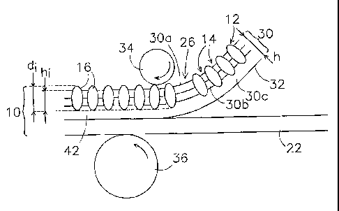
Fig. 2 illustrates an embodiment of the method for producing a
base material for screen-printing according to the invention. In
this Fig. 2, components which correspond to those shown in
Fig. I are denoted by the same reference designations. According
to the invention, the screen material 12, comprising dykes 16
which delimit screen openings 14, is firstly provided on one
side with a first resist layer, denoted overall by reference
numeral 30, which, by way of example, has been applied under
pressure in a number of steps, for example three steps, with the
aid of a squeegee coater. The partial layers are denoted by 30a,
b and c, respectively. As a result, a virtually uniform
thickness and penetration depth of the resist layer 30 in the
screen 12 is achieved, despite the fact that in this case too
there is a pinhole 26. There is a low risk of air inclusions if
the resist layer 30 is built up in substeps. A drying step is
carried out after application of the first resist layer parts
30a and 30b. Finally, a last partial layer 30c of resist
material is applied, to which the protective film 22 is applied
under a slight pressure while this partial resist layer 30c, or
at least the free surface 32 thereof, is still wet; in this
embodiment, the pressure is applied by pressure-exerting roll 34
CA 02743541 2011-06-20
- 15 -
with a surface consisting of hard rubber, and a counterpressure
roll 36 made from metal. After the assembly has been dried, the
result is a base material with a resist layer and a protective
film on one and the same side, with a smooth surface of the
resist layer 30, which has a uniform depth of penetration into
the screen 12. This depth of penetration or thickness is in this
figure denoted by hi between the contact surface 42
(corresponding to side 18 in the prior art) of the dykes 16 in
the resist layer 30 and the free surface of the resist layer 30
between the dykes 16. The total thickness of the resist layer 30
is denoted by h. The thickness of the screen 12 is denoted by di.
The filling level is more than 80%.
Fig. 3 shows an alternative method, in which the protective film
22 is also provided with an additional resist layer 38 of
photosensitive material, prior to lamination. In this case, the
lamination step is carried out while at least one side 32 and/or
40 of at least one of the resist layers 30 and 38 is wet.
Fig. 4 shows an embodiment of a device 100 according to the
invention. The device 100 comprises a frame (not shown), a
conveyor mechanism for moving screen material 12 in web form,
coating means for applying a (partial) layer 30, 30a-c of resist
material to one side of the screen material, drying means 102
for drying base material and/or screen material coated with
resist material, and joining means for applying protective film
to coated screen material. The conveyor mechanism comprises a
top winding unit 104 and a bottom winding unit 106. Each unit
may have a dedicated drive 105, so that a unit 104, 106 is
suitable for both unwinding and winding. In the embodiment
illustrated, the unit 104 is used to unwind a web 108 of screen
material 12 from a stock reel 110. Base material or screen
material coated with resist is being wound up at unit 106.
Furthermore, the conveyor mechanism comprises guide rolls 112
for guiding a web of material through the device 100. In the
embodiment illustrated, the coating means comprise a squeegee
device 114, comprising a knife box 116 on that side of the web
material which is to be coated, and a counterpressure knife 118
on the other side. The level of the resist material in the knife
CA 02743541 2011-06-20
I 4
- 16 -
box 116 is as far as possible kept constant in order to apply a
(partial) resist layer with a uniform thickness, advantageously
=
below the position of the tip of the counterpressure knife 118.
Drying of screen material coated with a partial resist layer is
carried out with the aid of IR dryers 102. Drying is not carried
out or not completely carried out after application of the last
partial resist layer, but rather protective film 22 in web form
which has been unwound from a stock reel 122 is partially guided
over a guide roll 112 and then brought into
contact with wet coated screen material. The guide roll 112 in
question in this case functions as a roll (denoted by
reference numeral 34 in Figs. 2 and 3). The base material 10
obtained in this way is wound up in the unit 106 and then dried.
Discharge means 124 are arranged above and below (although only
the latter is illustrated, for the sake of clarity) the path of
the protective film 22 from stock reel 122 to the guide
roll 112.
The method according to the invention achieves a very uniform
depth of penetration or filling level for the resist material,
which has been coated and protected on one side, in the screen,
as well as a very smooth surface of the resist layer in the base
material ultimately obtained.