Note: Descriptions are shown in the official language in which they were submitted.
CA 02743673 2011-06-16
1
POWER GENERATING SYSTEM
TECHNICAL FIELD
[0001] This disclosure generally relates to a power generating system which
interconnects an
inverter device and an alternating current commercial power source.
BACKGROUND DISCUSSION
[0002] A known power generating system for a cogeneration system is disclosed
in
JP2007-221916A (i.e., hereinafter referred to as Patent reference 1). The
power generating
system disclosed in the Patent reference 1 includes an engine driven by a
combustion of a fuel, a
generator actuated by the engine, a first converter converting an alternating
current power
generated by the generator into a direct current component, a second converter
converting the
direct current converted by the first converter into a alternating current
power for a load (load
alternating current power) and interconnected to a commercial power source as
a system, and a
control device controlling the first converter and the second converter. The
first converter and the
second converter construct an inverter device.
[0003] An alternating current of the load alternating current power outputted
by the second
converter of the inverter device occasionally includes a direct current
component. In those
circumstances, the direct current component may affect an operation of an
alternating current
power load connected to the inverter device. A guideline does not allow a
direct current
component to be included being equal to or greater than one percent (1%) of a
rated current. The
guideline requires to immediately disconnect (parallel off) the inverter
device from the system when
the alternating current of the load alternating current power outputted from
the inverter device
includes a direct current component equal to or greater than one percent.
According to an inverter
device for a small-sized cogeneration system, for example, in a case where 5A
of current is
outputted when 1kW of power is consumed, 5OmA is assumed to be a threshold
value (i.e.,
corresponding to one percent of the rated current). In those circumstances,
measurement that the
alternating current of the load alternating current power includes the direct
current component may
be assumed to be extremely difficult. A direct current-current transformer (DC-
CT) serving as an
electric current sensor as an electric current detection means is moderately-
priced as an electric
current detection sensor. However, there is a drawback that, according to the
DC-CT, a precision
of measurements is likely to be affected by the temperature and a temperature
drift is significant.
For example, according to the DC-CT serving as the electric current sensor,
there is a drawback
that the temperature drift Is generated because of the heat generation in use
of the system, errors
based on the temperature drift is added to detected values of the direct
current component, and the
direct current component included in the alternating current of the load
alternating current power is
not detected with high precision.
CA 02743673 2011-06-16
2
[0004] A need thus exists for a power generating system which is not
susceptible to the
drawback mentioned above.
SUMMARY
[0005] In light of the foregoing, the disclosure provides a power generating
system, which
includes an engine driven by a fuel, a generator actuated by the engine, an
inverter device including
a first converter converting an alternating current power generated by the
generator into a direct
current power, a second converter converting the direct current converted by
the first converter into a
load alternating current power and being interconnected with an alternating
current commercial
power source, and a gate drive circuit controlling a switching of the second
converter. The power
generating system further includes a control device including a control
portion having a central
processing unit and controlling the inverter device, a first current detection
device provided at the
second converter of the inverter device at a side closer to a load, the first
current detection device
detecting a load alternating electric current of the load alternating current
power converted by the
second converter, and a second current detection device provided between the
first converter and
the second converter of the inverter device, the second current detection
device detecting a direct
current of the direct current power converted by the first converter. The
control device obtains a first
integrated value which is calculated by integrating a direct current component
corresponding to a
positive electric current positioned at a positive side relative to a zero-
crossing of the load alternating
electric current among the direct current of the direct current power
converted by the first converter
and detected by the second current detection device by time, obtains a second
integrated value
which is calculated by integrating a direct current component corresponding to
a negative electric
current positioned at a negative side relative to the zero-crossing of the
load alternating electric
current among the direct current detected by the second current detection
device by time, and
detects a direct current component included in the load alternating electric
current of the load
alternating current power converted by the second converter on the basis of a
degree of a difference
between the first integrated value and the second integrated value.
BRIEF DESCRIPTION OF THE DRAWINGS
[00061 The foregoing and additional features and characteristics of this
disclosure will become
more apparent from the following detailed description considered with the
reference to the
accompanying drawings, wherein:
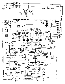
[0007] Fig. I is a system diagram illustrating a power generating system
according to a first
embodiment disclosed here;
[0008] Fig. 2A shows a waveform of a load alternating current outputted from a
second
converter of an inverter device and detected by a first electric current
sensor;
CA 02743673 2011-06-16
3
[0009] Fig. 2B shows a waveform of a direct current component outputted from a
first
converter of the inverter device when the load alternating current does not
include the direct current
component according to the first embodiment disclosed here;
[0010] Fig. 2C shows a waveform of a direct current component outputted from
the first
converter of the inverter device when the load alternating current includes
the direct current
component according to the first embodiment disclosed here;
[0011] Fig. 3 is a system diagram illustrating a power generating system
according to a
second embodiment disclosed here;
[0012] Fig. 4 illustrates waveforms of a timing voltage signal and command
current according
to the embodiments disclosed here;
[0013] Fig. 5 is a waveform chart showing timings of a first variable and a
second variable
current according to the embodiments disclosed here; and
[0014] Fig. 6 is a flowchart illustrating a process executed by a control
portion according to the
embodiments disclosed here,
DETAILED DESCRIPTION
[0015] Embodiments of a power generating system will be explained with
reference to
illustrations of drawing figures as follows.
[0016] An overview of the embodiment will be explained as follows. A control
device obtains
a first integrated value which is calculated by integrating a direct current
component corresponding
to a positive electric current positioned at a positive side relative to a
zero-crossing of the load
alternating electric current among the direct current of the direct current
power converted by a first
converter detected by a second current detection device by time. The control
device further
obtains a second integrated value which is calculated by integrating the
direct current component
corresponding to a negative electric current positioned at a negative side
relative to the
zero-crossing of the load alternating electric current by time. A degree of a
difference between the
first integrated value and the second integrated value corresponds to the
direct current component
included in the load alternating electric current of a load alternating power
converted by a second
converter. Thus, a control portion of the control device detects the direct
current component
included in the load alternating electric current of the load alternating
power converted by the
second converter based on the degree of the difference. An alternating voltage
signal which is
synchronized with the load alternating current power converted by the second
converter of an
Inverter device and is inputted to the control portion of the control device
via a transformer is defined
as a timing voltage signal Vp. In those circumstances, the control portion may
add an electric
voltage signal based on the difference between the first integrated value and
the second integrated
value plural times (e.g., 10 to 200 points) for each cycle of the timing
voltage signal Vp. An
increase of the added number of the electric voltage signal contributes to
enhance a resolution for a
CA 02743673 2011-06-16
4
detection accuracy when detecting the direct current component included in the
load alternating
power converted by the second converter.
[0017] A power generating system according to a first embodiment will be
explained with
reference to Figs. I and 2A-2C as follows. The power generating system
includes an engine 1
driven by fuel, a generator 2 rotated by the engine 1 to generate an electric
power, and an inverter
device 3. Exhaust heat produced by the engine 1 is sent to an engine coolant
circuit 10 to produce
warm water for a device 12 which uses warm-water, for example, a heater. The
inverter device 3
includes a first converter 30 which converts an alternating current power
generated by the generator
2 to a direct current component and a second converter 35 which converts the
direct current power
converted by the first converter 30 to an alternating current power for a load
(i.e., hereinafter
refereed to as a load alternating current power) and interconnects an
alternating current commercial
power source 43 and the second converter 35 as a system. The first converter
30 includes plural
first switching elements 31 converting the alternating current power generated
by the generator 2 to
the direct current component, and first flywheel (flyback) diodes 32. The
second converter 35 is
connected to the first converter 30 via wirings 30a, 30c and includes plural
second switching
elements 36 which converts the direct current power converted by the first
converter 30 into a load
alternating current power (alternating current power for a load) Wrn and a
second flywheel (flyback)
diode 37. A direct current intermediate voltage Vm at the wirings 30a, 30c
indicates a voltage at
an intermediate point between the first converter 30 and the second converter
35.
[0018] A gate signal So for turning on the second switching elements 36 of the
second
converter 35 is inputted into the second switching elements 36 from a gate
drive circuit 40. The
second converter 35 is interconnected to the alternating current commercial
power source 43 via
reactors 41, relays 42, the wirings 35a, 35c, and wirings 43a, 43b, 43c, or
the like as a system. An
indoor electric power load 47, for example, an electric power load 44, a lamp
45, and an induction
motor 46, or the like, is connected to an output of the inverter device 3 and
the alternating current
commercial power source 43 via the wiring 43a, 43b, 43c, respectively, so that
the electric power
load 44, the lamp 45, and the induction motor 46 are actuated in response to
the feeding of the
electric power from the alternating current commercial power source 43 and the
inverter device 3.
Wrings 48a, 48b, 48c, each of which is connected to the alternating current
commercial power
source 43 and the second converter 35 are connected to a transformer 48. A
first current sensor
59 (i.e., serving as a first current detection device) is provided at the
wiring 35c.
[0019] According to the embodiment, a voltage signal outputted from the
transformer 48 on
the basis of the alternating current commercial power source 43 and the second
converter 35 is
inputted to a control portion 50 from a first interruption port 503 and an A/D
(analog-to-digital) port
505 via an amplifier 48m and a filter 90 as a timing voltage signal VP. The
timing voltage signal Vp
corresponds to a signal informing timings of zero-crossings of a load
alternating current im of the
load alternating current power Wm, which is outputted from the second
converter 35 of the inverter
device 3, to the control portion 50.
CA 02743673 2011-06-16
[0020] A controller 5 includes the control portion (MPU) 50 including a CPU, a
phase locked
loop circuit (PLL circuit) 51 including an output port 513 outputting a
command current lp, a sine
wave generator 52 generating a sine wave signal based on the command current
ip outputted from
the output port 513 of the PLL circuit 51, a pulse-width modulation circuit
(PWM circuit) 53 to which
a sine wave signal Ic from the sine wave generator 52 is Inputted, and a phase
comparator 55.
The PLL circuit 51 includes the output port 513 connected to the PWM circuit
53 to output a signal
to the PWM circuit 53. In a case where the timing voltage signal Vp produced
by transforming the
voltage outputted from the second converter 35 by the transformer 48 is
inputted into the control
portion 50, an output frequency of the command current Ip supplied from the
output port 513 of the
PLL circuit 51 to the PWM circuit 53 increases at a power failure of the
alternating current
commercial power source 43. As shown in Fig. 1, the power generating system
includes an
electrically conductive path starting from the PLL circuit 51 to the PWM
circuit 53, the second
converter35, the transformer 48 and returning to the PLL circuit 51. The
control portion 50 includes
a CPU 501, a memory 502, the first interruption port 503, a second
interruption port 504 to which
the command current lpoutputted from the output port 513 of the PLL circuit 51
is inputted as an
Interrupting signal, the AID port 505, a digital-to-analog converter (D/A
converter) 57 converting a
digital signal to an analogue signal, and an analog-to-digital converter (A/D
converter) 58 which
converts the analog signal to the digital signal.
[0021] The phase comparator 55 includes a second input port 552 to which the
command
current Ip outputted from the output port 513 of the PLL circuit 51 is
inputted, a first input port 551 to
which the timing voltage signal Vp is inputted, and an output port 553. The
phase comparator 55
compares a phase of the command current Ip inputted from the second input port
552 and a phase
of the timing voltage signal Vp Inputted from the first input port 551. In a
case where the phase of
the timing voltage signal Vp is different from the phase of the command
current IF. the phase
comparator 55 outputs a phase difference signal Vr which is defined
proportionally to the phase
difference to the input port 511 of the PLL circuit 51 in order to resolve the
phase difference, The
PLL circuit 51 is configured to lock a phase of the command current I.
relative to a phase of the
timing voltage signal Vp in order to resolve the phase difference. In
consequence, a phase of the
command current Ip outputted from the output port 513 of the PLL circuit 51
can be set to be the
same phase to the phase of the timing voltage signal Vp. Thus, when the
inverter device 3 is
operated, the electric current outputted from the second converter 35 is
adjusted to have the same
phase to the timing voltage signal Vp, which is outputted from the second
converter 35 or the
alternating current commercial electric power 43 and inputted to the control
portion 50 from the
ports 503, 505 via the transformer 48, by the PLL circuit 51 and the PWM
circuit 53.
(0022] The PWM circuit 53 includes a triangular wave generator 531 generating
a triangular
wave voltage signal VK, a reference voltage generator 532 generating a
reference voltage signal Vh
which is defined proportionally to a level (value) of electric current of the
command current lp, and a
comparator 533 comparing the triangle wave voltage signal VK and the reference
voltage signal Vh.
CA 02743673 2011-06-16
6
The PWM circuit 53 outputs a control signal S, corresponding to the value of
the electric current of
the command current Ip to a gate drive circuit 40. Thus, the second switching
elements 36 of the
second converter 35 are controlled to be ON or OFF by the gate signal Sc from
the gate drive circuit
40 and the second converter 35 produces the load alternating current power Wm.
As shown in
Fig. 1, the timing voltage signal Vp is inputted to the first interruption
port 503 of the control portion
50 via a wiring 49a and is Inputted to the first input port 551 of the phase
comparator 55 via a wiring
55a. According to the construction of the embodiment, the inverter device 3
outputs the alternating
current im having the phase which is the same to the timing voltage signal Vp
from the second
converter 35 to the indoor electric power load 47.
10023] Further, as shown in Fig. 1, the control portion 50 of the controller 5
includes a D01
port 591, a D02 port 592, a D03 port 593, and an AID port 580 connected to the
AID converter 58.
A second electric current sensor (DC-CT2) 39 serving as a second current
detection device (direct
current detection means) is provided at the wiring 30c arranged between the
first converter 30 and
the second converter 35. For example, the second electric current sensor 39 is
constructed with a
Hall current transformer (Hall CT) which has a possibility to generate
temperature drift even though
a cost is lower. The second electric current sensor 39 is configured to detect
a direct current
component of the direct current power which is converted by the first
converter 30. The second
electric current sensor 39 outputs a detection signal Ir of direct current to
switching portions 71c,
72c of switching elements 71, 72. The switching element 71 turns on the
switching portion 71c on
the basis of a command signal D1 from the 001 port 591 of the control portion
50. The switching
element 72 turns on the switching portion 72c on the basis of a command signal
D2 from the D02
port 592 of the control portion 50.
(0024] As shown in Fig. 1, further, an integrator circuit 60 (differential
integrator circuit, gain
G1) is provided. The integrator circuit 60 includes a first operational
amplifier 61, a condenser 62
and a resistance 63 which are connected to an output terminal and an input
terminal of the first
operational amplifier 61, a resistance 64 connected to the first switching
portion 71c and the input
terminal of the operational amplifier 61, a resistance 65 connected to the
second switching portion
72c and the input terminal of the first operational amplifier 61, and a
resistance 66 and a condenser
67 which are connected to the input terminal of the operational amplifier 61.
An amplifier circuit 80
includes a second operational amplifier 81, a condenser 82 and a resistance 83
which are
connected to an output terminal and an input terminal of the second
operational amplifier 81. The
output terminal of the second operational amplifier 81 is connected to the A/D
converter 58 via a
wiring 81r and the A/D port 580 of the control portion 50. The output terminal
of the first
operational amplifier 61 is connected to the input terminal of the second
operational amplifier 81 via
a resistance 84.
(0025] According to the construction of the embodiment, as shown in Fig. 1, a
wiring 52r is
provided between the sine wave generator 52 and the PWM circuit 53. The first
electric current
sensor 59 (DC-CTI) serving as the first current detection device is provided
at the second converter
CA 02743673 2011-06-16
7
35 at a side closer to the indoor electric power load. The first electric
current sensor 59 is
constructed with a Hall current transfer (Hall CT) which has a possibility to
generate the
temperature drift although a cost is lower. The first electric current sensor
59 detects the load
alternating current im of the load alternating current power Wm which is
converted by the second
converter 35. An alternating current signal is which is a detection signal of
the first electric current
sensor 59 is inputted to the wiring 52r via a signal wire 59r. The wiring 52r
is connected to the
integrator circuit 60 via a wiring 52w and an analog switch (ASW) 52a. The
analog switch 52a is
switched by a command from the D03 port 593 of the control portion 50. The
analog switch 52a is
switched by the command from the D03 port 593 of the control portion 50 before
interconnecting to
the commercial power source 43, and I7t- is modified by a bias signal which is
adjusted to be zero
by a variable resistance. Thus, a drift over time and a failure of the first
electric current sensor 59
at an initial stage of the energization of the first electric current sensor
59 is detectable.
[0026] Fig. 2A shows a waveform of the alternating current im of the load
alternating current
power Wm which is detected as the alternating current is by the first electric
current sensor 59
which is provided at the second converter 35 of the inverter device 3 closer
to the indoor electric
power load. That is, Fig. 2A shows the alternating current im of the load
alternating current power
Wm converted by the second converter 35 of the inverter device 3. As indicated
with a
characteristic line W1 in Fig. 2, in a case where a direct current component
is not included in the
load alternating current im, the load alternating current im basically shows a
sine waveform and an
integrated value of a positive current positioned at a positive side relative
to a zero-crossing and an
integrated value of a negative current positioned at a negative side relative
to the zero-crossing are
the same. On the other hand, as indicated with a characteristic line W2 in
Fig. 2A, in a case where
a positive direct current component is included in the load alternating
current im, the alternating
current waveform is shifted to the positive side relative to the zero-
crossing, thus is offset relative to
the zero-crossing. Thus, in a case where the positive direct current component
is included in the
load alternating current im and the load alternating current im is offset, an
operation of a power load
driven by the alternating current may be Influenced, which is not favorable
and needs to be detected
at an early stage,
[0027] Fig. 2B shows a waveform of a direct current component detected by the
second
electric current sensor 39 in a case where the waveform of the load side
alternating current im
detected by the first electric current sensor 59 is normal (i.e., not offset)
as indicated with the
characteristic line W1 in Fig. 2A. In a case where the waveform of the load
side alternating current
im is normal without offset (i.e., the direct current component is not
included), as shown in Fig. 2B,
the direct current component converted by the first converter 30 forms two
arch shaped electric
current waves M1f, M2f. The electric current waves M1f, M2f basically
correspond timings and
waveform formed by full-wave rectifying the alternating current signal
detected by the first electric
current sensor 59 to the positive side. In a case where the waveform of the
load alternating
electric current im is not offset and is normal (i.e., the case where the
direct current component is
CA 02743673 2011-06-16
8
not included), dimensions (i.e,, integrated values integrated by time) of the
electric current
waveforms M1f, M2f shown in Fig. 2B as hatched portions are the same.
(00281 The electric current waveforms M1f, M2f are distributed by each half a
cycle by
commands DI, D2, respectively, from the DO1 port 591 and the D02 port 592 of
the control portion
50, a difference of the electric current integrated values of each of the half
cycle is obtained by the
integrator circuit 60, and the difference of the integrated values is
amplified by a gain G1. The gain
Cl may be set in accordance with a degree of the temperature drift of a zero
signal of the first
electric current sensor 59. The signal (analog signal) amplified by the degree
of the gain G1 is
further amplified at the amplifier circuit 80 by a gain G2, is inputted to the
A/D converter 58 of the
control portion 50 from the A/D port 580 of the control portion 50 via the
wiring 81 r, and is converted
to a digital signal. Thus, the voltage signal Vw inputted to the A/D converter
58 of the control
portion 50 corresponds to the difference of the integrated values of half
cycles of the direct current
component detected by the second electric current sensor 39 which is amplified
by the
multiplication of the gain G1 and the gain G2 (i.e., amplified by the gain G1
multiplied by the gain
G2). As illustrated in Figs. 2A-2B, in a case where the waveform of the load
alternating electric
current im detected by the first electric current sensor 59 (i.e., the
alternating current outputted from
the second converter 35 of the inverter device 3) does not include the direct
current component, an
integrated value sigma M1f (i.e., serving as a first integrated value)
obtained by integrating the
waveform M1f by time and an integrated value sigma M2f (i.e., serving as a
second integrated
value) obtained by integrating the waveform M2f by time are basically the
same, and thus a
difference between the integrated value sigma M1f and the integrated value
sigma M2f is assumed
to be zero.
[0029] On the other hand, Fig. 2C illustrates a direct current component
detected by the
second electric current sensor 39 in a case where the waveform of the load
alternating current im is
offset to the positive side as indicated with the characteristic line W2 in
Fig. 2A (i.e., the case where
the load alternating electric current im outputted from the second converter
35 of the inverter device
3 includes the direct current component). As shown in Fig. 2C, the direct
current component of the
direct current power which is converted by the first converter 30 forms
waveforms M 1 s, Mts.
Thus, in a case where the alternating electric current includes the direct
current component, an
integrated value sigma MIS (i.e., serving as a first integrated value)
obtained by integrating the
waveform M1s by time and an integrated value sigma M2s (i.e., serving as a
second integrated
value) obtained by integrating the waveform M2s by time are basically
different from each other.
The absolute value of the difference between the integrated value sigma M1s
and the integrated
value sigma M2s (i.e., IEM1s - EM2sl ) basically corresponds to a level of the
direct current
component included in the load alternating electric current im.
[0030] The voltage signal Vw obtained by amplifying the absolute value of the
difference of
the first and integrated values by the gain G1 multiplied by the gain G2 is
inputted to the A/D
converter 58 of the control portion 50 from the A/D port 580 of the control
portion 50 to be converted
CA 02743673 2011-06-16
9
to a digital signal. The control portion 50 detects the degree (level) of the
direct current component
included in the load alternating electric current im of the load alternating
current power Wm
converted by the second converter 35 of the inverter device 3. In those
circumstances, when the
temperature drift is generated at the first electric current sensor 59 and the
second electric current
sensor 39, the temperature drift affects (influences) both of the first
integrated value and the second
integrated value. Accordingly, even when the temperature drift is generated at
the first electric
current sensor 59 and the second electric current sensor 39, the temperature
drift is substantially
canceled. Thus, the direct current component included in the load alternating
electric current im of
the load alternating current power Wm converted by the second converter 35 of
the inverter device
3 is favorably detected. According to the construction of the embodiment, a
sensor which
generates the temperature drift is applicable as the first electric current
sensor 59 and the second
electric current sensor 39, and sensors with lower costs may be applicable.
[0031] The voltage signal Vw inputted from the A/D port 580 to the A/D
converter 58 of the
control portion 50 is assumed to have a value multiplying the difference of
the integrated values of
half cycles (i.e., the difference between the first and second integrated
values) of the second
electric sensor (DC-CT2) 39 by a gain (G1 x G2). The voltage signal Vw is
inputted to the control
portion 50 including a CPU from the AID port 580 via the A/D converter 58 by
plural points (i.e.,
plural times) per a cycle of the timing voltage signal Vp (see Fig.4) by means
of a software, and are
added as a digital signal at the control portion 50. For example, the voltage
signal Vw is inputted
to the A/D converter 58 of the control portion 50 via the A/D port 580 by 60
points for each cycle of
the timing voltage signal Vp, is converted from an analog signal to digital
signal (A/D conversion),
and is added at the control portion 50. The number of Inputting times (e.g.,
60 points) is
determined for detecting direct current components with adequate precision
even with a lower cost
CPU having an A/D converter (corresponding to the A/D converter 58) whose
resolution is around
bit.
[0032] In those circumstances, in a case where the AID converter whose
resolution is around
10 bit is applied as the AID converter 58 provided at the control portion 50,
an electric current value
applied per 1 bit is assumed to be relatively large compared to an AID
converter having greater bit
and a detection of the direct current components with high precision may
become difficult. For
example, in a case where it is determined that the alternating current im is
abnormal because a
direct current component is included in the alternating current im outputted
from the inverter device
3 when a direct current component to be detected exceeds a range of 5OmA
(i.e., corresponding to
a threshold of one percent in a case where 5A of current is outputted when 1
kW of power is
consumed) with the resolution around 10 bit, assuming the electric current
value per I bit is
approximately 20mA, SOmA corresponding to a threshold value falls within the
range of 41mA to
59mA, which makes it difficult to detect the direct current component included
in the alternating
current im outputted from the inverter device 3.
CA 02743673 2011-06-16
[0033] According to the embodiment, n times (e.g., 60 times) data is added at
the control
portion 50 per one cycle of the timing voltage signal Vp. When detecting the
direct electric current,
the resolution increases by the added numbers of times (n times). Adding the
voltage signal Vw,
for example, 60 times connotes that the resolution at the control portion 50
is assumed to be 60
times greater. In those circumstances, when 60 times are added, basically, the
resolution at the
control portion 50 is assumed to be 20mA 160 = 0.33mA, and thus the degree of
the direct current
around 50mA can be judged with the resolution being equal to or less than 1
mA. Thus, the
precision for detecting that the direct current component is included in the
alternating current im is
enhanced even though the resolution of the AID converter is relatively low
according to the
constructions of the embodiment. The added number of times (n times) is not
limited to 60 times.
Depending on cases, the added number of times (n times) may be determined in a
range of 10-200
times, 15-100 times, or the like.
[0034] A second embodiment will be explained with reference to Fig. 3. The
basic
construction of the second embodiment is common to the first embodiment, and
the same
advantages and effects to the first embodiment are obtained. Likewise, the
waveforms and
characteristics shown in Figs. 2A-2C are applied to the second embodiment. As
shown in Fig. 3,
the integrator circuit 60 and the amplifier circuit 80 are provided. According
to the second
embodiment, likewise the first embodiment, the electric current waveforms M1f,
M2f, MIs, M2s are
distributed by each half cycle by the commands D1, D2, respectively, from the
DOI port 591 and
the D02 port 592 of the control portion 50, a difference of the electric
current integrated values of
each of the half cycle is obtained by the integrator circuit 60, and the
difference is amplified by a
degree of the gain G1. The gain G1 may be determined in accordance with the
degree of the
temperature drift of the zero signal of the first electric current sensor 59.
Then, the signal (i.e.,
analog signal) amplified by the degree of the gain G1 is further amplified at
the amplifier circuit 80
by the gain G2, inputted to the A/D converter 58 of the control portion 50 via
the wiring 81 r and the
A/D port 580 to be converted to a digital signal. The voltage signal Vw
inputted from the A/D port
580 to the A/D converter 58 of the control portion 50 corresponds to the
difference of the integrated
values of the half cycles (i.e., the difference of the first and second
integrated values) of the direct
current component detected by the second electric current sensor 39 which is
amplified by the
multiplication of the gain G1 and the gain G2 (i.e., gain GI x gain G2
[0035] Based on the voltage signal Vw obtained by amplifying the absolute
value of the
difference of the first and second integrated values by the multiplication of
the gain G1 and the gain
G2, the control portion 50 detects the degree of the direct current component
included in the load
alternating current im of the load alternating current power Wm converted by
the second converter
35 of the inverter device 3. In those circumstances, the data of n times
(e.g., 60 times) may be
added at the control portion 50 for each cycle of the timing voltage signal
Vp. When detecting the
direct current, the resolution is increased by the added number of times (n
times). In those
circumstances, when the temperature drift is generated at the first electric
current sensor 59 and the
CA 02743673 2011-06-16
11
second electric current sensor 39, an error in a detected value of the direct
current component due
to the temperature drift influences on both of the first integrated value and
the second integrated
value. Thus, even when the temperature drift is generated at the first
electric current sensor 59
and the second electric current sensor 39, an error in a detected value of the
direct current
component by the temperature drift is substantially canceled at the difference
of the first and second
integrated values. Accordingly, the direct current component included in the
load alternating
current im of the load alternating current power Wm converted by the second
converter 35 of the
inverter device 3 is favorably detected. As explained above, according to the
constructions of the
embodiment, a sensor that may generate the temperature drift is applicable as
the first electric
current sensor 59 and the second electric current sensor 39, and thus a
manufacturing cost is
reduced.
[0036] Further, referring to Figs. 4 and 5 constructions of the embodiments
will be explained.
The constructions shown in Figs. 4 and 5 are applicable to the first and
second embodiments, and
thus are applicable to Figs. I to 3. When the temperature drift is generated
at the first electric
current sensor 59 and the second electric current sensor 39, the temperature
drift influences on
both of the first Integrated value and the second integrated value. Thus, even
when the
temperature drift is generated at the first electric current sensor 59 and the
second electric current
sensor 39, the temperature drift is substantially canceled. Accordingly, the
direct current
component included in the load side alternating current im of the load
alternating current power Wm
which is converted by the second converter 35 of the inverter device 3 is
favorably detected.
Namely, according to the constructions of the embodiment, a sensor that may
generate the
temperature drift is applicable as the first electric current sensor 59 and
the second electric current
sensor 39, and thus a manufacturing cost is reduced. According to the
embodiments, a power
outage of the alternating current commercial power source 43 during the
inverter device 3 is in
operation is detected. Fig. 4 shows a state where the timing voltage signal Vp
and the command
current lp have the same phase as a wavelength. The timing voltage signal Vp
is inputted to the
first interruption port 503 of the control portion 50 and includes the same
phase with the phase of
the load alternating current power Wm outputted from the second converter 35
of the inverter
device 3 and the alternating current commercial power source 43 via the
transformer 48. The
command current lp is outputted from the output port 513 of the PLL circuit 51
to the sine wave
generator 52. As shown in Fig. 4, a cycle T corresponding to a wavelength of
the timing voltage
signal Vp corresponds to a counter value N (e.g., N = 10000) of a counter
provided at the control
portion 50. Counting of the counter value N by the control portion 50 starts
from a zero-crossing
Vo of the timing voltage signal Vp. For example, in a case where the phase of
the command
current Ip relative to the phase of the timing voltage signal Vp is delayed
(displaced) by 90 degrees,
the phase difference of 90 degrees corresponds to N/4 of the counter value. In
a case where the
phase of the command current Ip relative to the phase of the timing voltage
signal Vp is delayed
(displaced) by 3 degrees, the phase difference of 3 degrees corresponds to
N/120 of the counter
CA 02743673 2011-06-16
12
value. In a case where the phase of the command current Ip relative to the
phase of the timing
voltage signal Vp is delayed (displaced) by 15 degrees, the phase difference
of 15 degrees
corresponds to the N/24 of the counter value. In other words, in a case where
the phase of the
command current lp relative to the phase of the timing voltage signal Vp is
delayed (displaced) by D
degree(s), the phase difference of D degree(s) corresponds to N/(360/D) of the
counter value. As
described above, the phase comparator 55 and the control portion 50 are
configured to obtain the
phase difference of the command current Ip relative to the timing voltage
signal Vp on the basis of
the counter value.
[0037] According to the embodiments, in a case where the alternating current
commercial
power source 43 and the inverter device 3 are interconnected with each other,
the control portion 50
of the control device 5 instantaneously inputs a pulse signal Sc, whose pulse
is in a rectangular
shape (see Fig. 3), into a second input port 512 of the PLL circuit 51 from an
output port 570 of the
D/A converter 57 for a predetermined time At1 (e.g. 200 milliseconds), in
order to forcibly and
instantaneously displace (fluctuate) the phase of the command current Ip by a
first variable (e.g., by
three degrees (3 )) relative to the timing voltage signal Vp in a
predetermined cycle (e.g. any value
within a range of 10 to 2000 milliseconds), thereby intentionally generating a
fluctuation to a
reactive power. Accordingly, the PLL circuit 51 supplies the command current
IQ to the sine wave
generator 52 from the output port 513 as a signal defining a phase timing. The
sine wave
generator 52 outputs a signal, which has a wave height value (i.e. a current
value) corresponding to
the direct current intermediate voltage V, of the inverter device 3, as a
current command value Ic
while following the phase timing based on the command current lp. The PWM
circuit 53 compares
the current command value Ic and an actual current value Ir inputted into the
PWM circuit 53 from
the current sensor 59. Then, the PWM circuit 53 outputs a current, whose phase
is forcibly
displaced by three degrees (3 ) relative to the timing voltage signal Vp, to
the gate drive circuit 40.
Then, after the predetermined time At1 has elapsed, the control portion 50 of
the control device 5
Inputs a signal Ss for adjusting the phase of the command current Ip to have
the same phase as the
timing voltage signal Vp into the second input port 512 of the PLL circuit 51
from the output port 570
of the D/A converter 57 for a predetermined time At2 (e.g. 200 milliseconds).
Accordingly, the
command current IF. is adjusted to have the same phase as the timing voltage
signal Vp.
[0038] In the case where the phase of the command current Ip Is forcibly
displaced by three
degrees (3 ) relative to the timing voltage signal Vp, the control portion 50
determines whether or
not the phase difference of the command current Ir, relative to the timing
voltage signal Vp is actually
three degrees (3 ) on the basis of the counter value. In those circumstances,
while the alternating
current commercial power source 43 is in a normal state (i.e. while the
commercial power supply 43
does not fail), the obtained phase difference is expected to fall within a
range of a threshold value
corresponding to three degrees. Therefore, the control portion 50 determines
that no power
outage occurs at the alternating current commercial power source 43. However,
in a case where
the power outage occurs at the alternating current commercial power source 43,
the phase
CA 02743673 2011-06-16
13
difference corresponding to three degrees is not likely to be obtained, so
that the phase difference
falls outside of the range of the threshold value corresponding to three
degrees. Accordingly, in
the case where the phase difference of the command current Ip relative to the
timing voltage signal
Vp falls outside of the range of the threshold value use for the phase
difference, the control portion
50 of the control device 5 temporarily determines a possibility of the power
outage at the alternating
current commercial power source 43. At a timing when a temporal determination
of the power
outage by the control device 5 is concluded, which serves as a trigger, the
control portion 50 of the
control device 5 outputs the signal S8 for forcibly and rapidly raise the
command current Ip by a
second variable (e.g., fifteen degrees (15 )), which is greater than the first
variable, so as to
fluctuate the phase of the command current Ip relative to the timing voltage
signal Vp, to the PLL
circuit 51 from the output port 570 of the D/A converter 57. In this case, in
a case where no power
outage occurs at the alternating current commercial power source 43, changes
in frequency of the
timing voltage signal Vp fall within a threshold value used for the frequency
and are relatively small.
Furthermore, in this case, the phase difference of the command current Ip
relative to the timing
voltage signal Vp falls within the range of the threshold value used for the
phase difference and is
relatively small. Accordingly, the control portion 50 of the control device 5
determines that there is
no possibility of the power outage occurring at the alternating current
commercial power source 43.
In a case where the alternating current commercial power source 43 fails while
the induction motor
46 is rotatably driven, the induction motor 46 continues to rotate by its
inertia so as to function as an
induction generator although the alternating current commercial power source
43 fails, which may
result in applying the voltage to the alternating current commercial power
source 43. Accordingly,
fluctuation in the frequency of the timing voltage signal V, may not occur.
[0039] In the embodiments, in a case where the second variable is greater and
where the
alternating current commercial power source 43 fails, the changes in the
frequency of the timing
voltage signal Vp follow a degree (a level) of the second variable, so that
the changes in the
frequency of the timing voltage signal Vp fall outside of the range of the
threshold value used for the
frequency. Furthermore, in the case where the power outage occurs at the
alternating current
commercial power source 43, the PLL circuit 51 generates a relatively great
fluctuation in the
frequency of the timing voltage signal Vp, because the PLL circuit 51 is
configured so that the
frequency of the command current l p outputted from the output port 513
increases in the case of the
power outage. The fluctuation of the frequency is set to have a degree so as
to overcome the
inertia of the Induction motor 46. Furthermore, while the power outage occurs
at the alternating
current commercial power source 43, the phase difference of the command
current Ip relative to the
timing voltage signal Vp follows the degree of the second variable so as to
fall outside of the
threshold value used for the phase difference.
[0040] Accordingly, in the case where the frequency of the timing voltage
signal Vp falls
outside of the threshold value used for the frequency and further, in the case
where the phase
difference falls outside of the threshold value used for the phase difference,
the control portion 50 of
CA 02743673 2011-06-16
14
the control device 5 conclusively determines that the alternating current
commercial power source
43 fails. According to the first embodiment, in the case where the inverter
device 3 is actuated
while being interconnected to the alternating current commercial power source
43 as described
above, the control portion 50 of the control device 5 inputs the signal So for
generating the phase
difference of three degrees at the phase of the command current Ip relative to
the timing voltage
signal Vp (by the first variable) in a predetermined cycle into the second
input port 512 of the PLL
circuit 51 from the D/A converter 57 at the predetermined cycle (At1, At2).
Furthermore, the
control portion 50 detects the phase difference between the command current ip
and the timing
voltage signal Vp, so that the control portion 50 determines that the
alternating current commercial
power source 43 does not fail in the case where the phase difference
corresponds to three degrees.
Accordingly, the control portion 50 temporarily and periodically (At1, At2)
determines the possibility
of the power outage of the alternating current commercial power source 43. In
a case where the
power outage actually occurs at the alternating current commercial power
source 43, the phase
difference of the command current Ip relative to the timing voltage signal V p
does not correspond to
three degrees (3 ) because the voltage of the alternating current commercial
power source 43 is lost
when the power outage occurs at the alternating current commercial power
source 43. Therefore,
the control portion 60 of the control device 5 inputs the signal Sc for
generating the phase difference
of fifteen degrees (15 ) at the command current I p relative to the timing
voltage signal Vp (by the
second variable) into the second input port 512 of the PLL circuit 51 from the
output port 570 of the
D/A converter 57 at the timing when the power outage occurs at the alternating
current commercial
power source 43 as a trigger. Accordingly, the reactive power increases, so
that a balance between
the output and the load is lost and the direct current intermediate voltage Vm
fluctuates, which results
in greatly fluctuating the command current IF. relative to the timing voltage
signal Vp. As a result, a
voltage root means square value (i.e. a voltage RMS value) of the timing
voltage signal Vp also
fluctuates and the phase of the command current Ip relative to the timing
voltage signal Vp greatly
changes. Therefore, in a case where the voltage RMS value of the timing
voltage signal Vp falls
outside of the range of the threshold value and where the phase difference of
the command current
Ip relative to the timing voltage signal Vp falls outside of the range of the
threshold value used for the
phase difference, the control device 5 conclusively determines that the power
outage occurs at the
alternating current commercial power source 43.
10041] The PLL circuit 51 is configured so that the frequency of the current
outputted from the
output port 513 of the PLL circuit 51 automatically increases in the case that
the power outage
occurs at the alternating current commercial power source 43. Therefore, in a
case where the
frequency of the timing voltage signal Vp falls outside of the range of the
threshold value used for
the frequency, the control device 5 conclusively determines that the power
outage occurs at the
alternating current commercial power source 43. Accordingly, a determination
accuracy of the
occurrence of the power outage of the alternating current commercial power
source 43 is increased.
CA 02743673 2011-06-16
[0042] Even In the case where the command current Ip is displaced by fifteen
degrees (by the
second variable) relative to the timing voltage signal Vp, the control device
5 determines that the
power outage does not occur at the alternating current commercial power source
43 if the
fluctuation of the timing voltage signal VP falls within the range of the
threshold value used for the
phase difference. Accordingly, a misdetermination of the power outage of the
alternating current
commercial power source 43 is avoided.
[0043] A detailed process executed by the control portion 50 of the control
device 5 will be
described below with reference to Fig. 6. The process executed by the control
portion 50 of the
control device 5 shown in Fig. 6 is applicable to the first and second
embodiments. When the
temperature drift is generated at the first electric current sensor 59 and the
second electric current
sensor 39, the temperature drift influences on both of the first integrated
value and the second
integrated value. Thus, even when the temperature drift is generated at the
first electric current
sensor 59 and the second electric current sensor 39, the temperature drift is
substantially canceled.
Accordingly, the direct current component included in the load alternating
current im of the load
alternating current power Wm converted at the second converter 35 of the
inverter device 3 is
favorably detected. This allows that a sensor which generates the temperature
drift is applied as
the first electric current sensor 59 and the second electric current sensor
39, which contributes to a
cost reduction.
[0044] According to the embodiments, a power outage of the alternating current
commercial
power source 43 during the inverter device 3 is in operation is detected. As
illustrated in Fig. 6, in
a case where the inverter device 3 is actuated so as to generate a
predetermined output while being
interconnected to the alternating current commercial power source 43, the
control portion 50 of the
control device 5 executes a process of inputting the signal Sc for displacing
the command current Ip
by three degrees (3 ) (by the first variable) relative to the timing voltage
signal Vp in the
predetermined cycle Into the second input port 512 of the PLL circuit 51 from
the output port 570 of
the D/A converter 57 (step S101). Then, the control portion 50 obtains the
phase difference of the
command current Ip relative to the timing voltage signal Vp (step $102). In
the case where the
phase difference corresponding to three degrees (3 ) is obtained (No in step
S103), the control
device 5 temporarily determines that the commercial power supply 43 is in the
normal state and the
power outage does not occur at the alternating current commercial power source
43. Then, the
process returns to step S101. In the case where the power outage occurs at the
alternating
current commercial power source 43, the phase difference of the command
current lp relative to the
timing voltage signal Vp does not correspond to three degrees (3 ) (Yes in
step S103). Therefore,
in this case, the control portion 50 temporarily determines that the power
outage occurs at the
alternating current commercial power source 43 (step S104).
(0045] Using the temporal determination as the trigger, the control portion 50
of the control
device 5 executes a process of inputting the signal Sc for displacing the
command current ip so as
by fifteen degrees (15 ) (by the second variable) relative to the timing
voltage signal Vp into the
CA 02743673 2011-06-16
16
second input port 512 of the PLL circuit 52 from the output port 570 of the
D/A converter 57 (step
S105). Accordingly, the reactive power increases, which results in losing the
balance between the
output and the load. In this case, the direct current Intermediate voltage Vm
fluctuates and the
timing and fluctuation in a waveform of each of the timing voltage signal Vp
and the command
current Ip increase. As a result, the voltage RMS value of the timing voltage
signal VP also
fluctuates. Furthermore, the phase of the command current Ip relative to the
timing voltage signal
V1. also greatly changes. Therefore, the control portion 50 obtains the
changes (the fluctuation) of
the voltage RMS value of the timing voltage signal Vp (step S106), In the case
where the
fluctuation of the voltage RMS value of the timing voltage signal Vp falls
outside of the range of the
threshold value (Yes in step S107), the control portion 50 conclusively
determines that the power
outage occurs at the alternating current commercial power source 43 (step
S112). Furthermore,
the control device 5 executes a process of breaking electricity to the
alternating current commercial
power source 43, such as cutting the interconnection between the alternating
current commercial
power source 43 and the inverter device 3 (step S113).
[0046] The PILL circuit 51 is configured so that the frequency of the command
current Ip
outputted from the output port 513 of the PLL circuit 51 automatically
increases in the case where
the power outage actually occurs at the alternating current commercial power
source 43.
Accordingly, in the embodiments, the control portion 50 obtains the
fluctuation of the frequency of
the timing voltage signal Vp (step S108) even in the case where the voltage
RMS value of the timing
voltage signal Vp falls within the range of the threshold value used for the
voltage RMS value (No in
step $107), in order to increase accuracy in the detection of the occurrence
of the power outage at
the alternating current commercial power source 43. In the case where the
fluctuation of the
frequency falls outside of the range of the threshold value used for the
frequency (Yes in step
S109), the control device 5 conclusively determines that the power outage
occurs at the alternating
current commercial power source 43 (step 8112) and then executes the process
of cutting the
electricity to the alternating current commercial power source 43 (step S113).
10047 The control portion 50 obtains the phase difference of the command
current Ip relative
to the timing voltage signal Vp (step S110) even in the case where the
fluctuation of the frequency
falls within the range of the threshold value used for the frequency (No in
step S109). In the case
where the phase difference falls outside of the range of the threshold value
(Yes in step S111), the
control portion 50 conclusively determines that the power outage occurs at the
alternating current
commercial power source 43 (step S112). Then, the control portion 50 executes
the process of
breaking the electricity to the alternating current commercial power source 43
such as cutting the
interconnection between the alternating current commercial power source 43 and
the inverter
device 3 (step S113). On the other hand, in the case where the fluctuation of
the frequency falls
within the range of the threshold value use for the frequency (No in step
5109) and where the phase
difference of the command current lp relative to the timing voltage signal Vp
falls within the range of
the threshold value (No in step S111), the control portion 50 determines that
the power outage does
CA 02743673 2011-06-16
17
not occur at the alternating current commercial power source 43 and the
process returns to step
$101.
[0048] According to the embodiment, in the case where the possibility of the
power outage at
the alternating current commercial power source 43 is temporarily determined
to be high, the control
portion 50 generates the phase difference (by the second variable) between the
command current
Ip and the timing voltage signal Vp and then, the control portion 50
determines whether or not the
power outage occurs at the alternating current commercial power source 43 on
the basis of plural
parameters. Accordingly, the misdetermination of the power outage at the
alternating current
commercial power source 43 may be restrained. Any selective desired values, by
which the
possibility of the power outage at the commercial power supply 43 is
determined on the basis of an
actuating state of each of the inverter device 3 and the alternating current
commercial power source
43 and the like, may be adapted as the threshold value of each parameter.
According to the
embodiments, in the case where the phase difference is generated on the basis
of the second
variable, the voltage RMS value of the timing voltage signal Vp, the
fluctuation of the frequency of the
timing voltage signal Vp and the phase difference of the command current lp
relative to the timing
voltage signal Vp are obtained In the above-mentioned order. However, the
power generating
system according to the embodiments may be modified so that the fluctuation of
the frequency of the
timing voltage signal Vp, the voltage RMS value of the timing voltage signal
Vp, the phase difference
of the command current Ip relative to the timing voltage signal Vp, the
fluctuation of the frequency of
the timing voltage signal Vp and the voltage RMS value of the timing voltage
signal Vp may be
obtained in the above-mentioned order.
[0049] In the above-mentioned embodiments, the first variable is set to
generate the phase
difference 4)1 of three degrees (3 ) between the command current lp and the
timing voltage signal
Vp and the second variable is set to generate the phase difference 4>2 of
fifteen degrees (15 )
between the command current Ip and the timing voltage signal Vp. However, the
first variable may
be set to generate a phase difference 41 which falls within a range between,
for example, two to
seven degrees (2 to 7 ), between the command current lp and the timing
voltage signal Vp and the
second variable may be set to generate a phase difference +2 in a range
between, for example, ten
to twenty degrees (10 to 20 ). Ina case where the second variable is set to
be excessively great,
a strain of the timing voltage signal VP may become unfavorably excessive.
Therefore, a value
obtained by dividing the second variable by the first variable (4)2 /4)1) may
be set to wall within a
range between 2.5 to 7 or between 3 to 6. The power generating system
according to this
disclosure is not limited to the above-described embodiments and drawings. The
power
generating system according to this disclosure may be changed or modified
without departing from
the spirit and scope of this disclosure.
[0050] According to the embodiments, the power generating system includes the
engine 1
driven by a fuel, the generator 2 actuated by the engine 1, the inverter
device 3 including the first
converter 30 converting the alternating current power generated by the
generator 2 into the direct
CA 02743673 2011-06-16
18
current power, the second converter 35 converting the direct current converted
by the first converter
30 into the toad alternating current power and being interconnected with the
alternating current
commercial power source 43, and the gate drive circuit 40 controlling the
switching of the second
converter 35. The power generating system further includes the control device
5 including the
control portion 50 having the central processing unit and controlling the
inverter device 3, the first
current sensor 59 provided at the second converter 35 of the inverter device
at a side closer to the
toad, the first current sensor 59 detecting the load alternating electric
current of the load alternating
current power converted by the second converter 35, and the second current
sensor 39 provided
between the first converter 30 and second converter 35 of the inverter device
3, the second current
sensor 39 detecting the direct current of the direct current power converted
by the first converter 30.
The control device 5 obtains the first integrated value M1f, M1s which is
calculated by integrating the
(a) direct current component corresponding to a positive electric current
positioned at a positive side
relative to a zero-crossing of the load alternating electric current among the
direct current of the
direct current power converted by the first converter 30 detected by the
second current sensor 39 by
time, obtains the second integrated value M2f, M2s which is calculated by
integrating a direct current
component corresponding to a negative electric current positioned at a
negative side relative to the
zero-crossing of the load alternating electric current, and detects a direct
current component
included in the load alternating electric current of the load alternating
current power converted by the
second converter 35 on the basis of a degree of a difference between the first
integrated value and
the second integrated value.
[00513 According to the embodiments, first current sensor 59 (the first
current detection
device) is provided at the second converter of the inverter device at a side
closer to the load, and
detects the load alternating current of the load alternating power converted
by the second converter
35 of the inverter device 3. The second current sensor 39 (the second current
detection device) is
provided between the first converter 30 and the second converter 35 to detect
the direct current
component of the direct current power converted by the first converter 30. The
control device 5
obtains the first integrated value M1f, M1s which is calculated by Integrating
the direct current
component corresponding to the positive electric current positioned at the
positive side relative to the
zero-crossing of the load alternating electric current among the direct
current component detected
by the second current sensor 39 by time. The control device 5 further obtains
the second
integrated value M2f, M2s which is calculated by integrating the direct
current component
corresponding to the negative electric current positioned at the negative side
relative to the
zero-crossing of the load alternating electric current among the direct
current detected by the
second current sensor 39 by time. The control device 5 detects the direct
current component
included in the load alternating current of the load alternating power
converted by the second
converter 35 on the basis of the degree of the difference between the first
integrated value M1f, M1 s
and the second integrated value M2f, M2s. In those circumstances, when the
temperature drift is
generated at the first current sensor 59 and the second current sensor 39, the
temperature drift
CA 02743673 2011-06-16
19
Influences on both of the first integrated value M1f, MIs and the second
integrated value M2f, M2s.
Thus, even when an error based on the temperature drift is generated at the
first current sensor 59
and the second current sensor 39, the temperature drift is substantially
cancelled at the difference,
and the error based on the temperature drift is substantially cancelled.
Accordingly, the direct
current component included in the load alternating current of the load
alternating power converted
by the second converter 35 is favorably detected. The temperature drift
defines that the precision
in detection of the electric current declines due to the temperature.
According to the construction
of the embodiments, a current sensor which generates the temperature drift is
applicable as the first
current sensor 59 and the second current sensor 39.
[0052] According to the construction of the embodiments, when the load
alternating current
power converted by the second converter 35 of the inverter device 3 is
outputted to the load, the
control device 5 detects the direct current component included in the load
alternating current of the
load alternating current power converted by the second converter 35 on the
basis of the degree of
the difference between the first integrated value Mlf, MIs and the second
integrated value M2f,
M2s. In those circumstances, even when the first current sensor 59 and the
second current sensor
39 are likely to be influenced by the temperature drift, the direct current
component included in the
load alternating current of the load alternating current power converted by
the second converter is
favorably detected.
[0053] According to the embodiments, the power generating system includes the
transformer
48. The control portion 5 adds a voltage signal based on the difference
between the first integrated
value M1f, MIs and the second integrated value M2f, M2s for multiple times
during a cycle of a
timing voltage signal Vp when the timing voltage signal Vp is defined as an
alternating current
voltage signal inputted to the control portion 50 of the control device 5 via
the transformer 48 and is
synchronized with the load alternating current power converted by the second
converter 35 of the
inverter device 3.
[0054] Further, according to the embodiments, the load includes the indoor
electric power load
47 which is connected to an output of the alternating current commercial power
source 43 and an
output of the inverter 3.
[0055] Still further, according to the embodiments, the indoor electric power
load 47 includes
the induction motor 46.
[00561 The principles, preferred embodiment and mode of operation of the
present invention
have been described in the foregoing specification. However, the invention
which is intended to be
protected is not to be construed as limited to the particular embodiments
disclosed. Further, the
embodiments described herein are to be regarded as illustrative rather than
restrictive. Variations
and changes may be made by others, and equivalents employed, without departing
from the spirit of
the present Invention. Accordingly, it Is expressly intended that all such
variations, changes and
equivalents which fall within the spirit and scope of the present invention as
defined in the claims, be
embraced thereby.