Note: Descriptions are shown in the official language in which they were submitted.
CA 02744111 2011-05-18
a
METHOD AND DEVICE FOR OPTICAL SWITCHING
[0001] The application claims priority to Chinese Patent Application No.
200810177646.1,
filed on November 20, 2008, and entitled "METHOD AND DEVICE FOR OPTICAL
SWITCHING", which is incorporated herein by reference in its entirety.
FIELD OF THE TECHNOLOGY
[0002] The present invention relates to the field of communications
technology, and more
particularly to a method and a device for optical switching.
BACKGROUND OF THE INVENTION
[0003] The current dense wavelength division multiplexing (DWDM) technologies
enable
one optical fiber to accommodate hundreds of wavelengths, and each wavelength
has a
transmission rate of up to 40 Gbit/s or even 100 Gbit/s, and the capacity of
one optical fiber
is up to the magnitude of Tbit/s, meeting demands for network bandwidth.
Meanwhile, the
DWDM technologies make the network cost and the control complexity increased
significantly. As the number of the wavelengths accommodated in an optical
fiber is up to
hundreds, the number of ports for optical fiber switching and wavelength
switching in
optical cross-connect (OXC) is largely increased, and the cost of the optical
switching is
increased significantly. At the same time, the larger the scale of the OXC is,
the more
difficult and complex the control of the OXC will be. It is assumed that 20
input optical
fibers and 20 output optical fibers are provided at a node, and 100
wavelengths are
transmitted in each optical fiber simultaneously; if a common OXC node is
used, 2000
input ports, 2000 output ports, and a 2000 x 2000 optical switch matrix are
needed,
resulting in high cost and complexity of the OXC. Furthermore, the development
of a
network towards a dynamic full mesh network has higher requirements on the
dimension of
service signals. Due to the dynamic and flexible property of the network, the
wavelengths
are dispatched with time, and at different time points, the dimension of the
wavelengths that
needs to be switched is different, so that higher requirements are made on the
dimension of
1
CA 02744111 2011-05-18
service signals. Therefore, a switching structure capable of realizing
multiple granularities
and multiple dimensions, having extensibility, and capable of being flexibly
upgraded is of
great importance for the construction and management of a dynamic network.
[0004] In order to solve the problem of increased switching cost and control
complexity
caused by the development of the optical network technology, a multi-
granularity optical
switching technology is set forth. The multi-granularity optical switching
technology means
to perform optical fiber switching, waveband switching, and wavelength
switching
simultaneously in the same optical node. The waveband switching refers to that
multiple
wavelengths form a waveband for performing switching as a unit, reducing the
number of
ports needed for switching, and decreasing the cost. Meanwhile, three
switching
granularities, that is, optical fiber, waveband, and wavelength, are provided,
which can be
adjusted flexibly according to service requirements, thereby reducing the
control
complexity.
[0005] The multi-granularity optical switching technology can be realized by
an optical
switching structure with a multiplexer and demultiplexer (DEMUX) loopback. The
solution
can dynamically switch and transparently transmit the added/dropped wavebands
and
wavelengths. Each output port of the DEMUX loopback has cycle passbands, and
therefore
any waveband can be demultiplexed into single wavelengths. The DEMUX divides
an input
DWDM channel into wavebands and directly sends the wavebands to an optical
switch, and
then the optical switch dispatches the wavelengths according to requirements.
The solution
can realize optical fiber-level, wavelength-level, and waveband-level
switching.
[0006] However, in practice, not all the wavelengths need to be demultiplexed
into single
wavelengths by the DEMUX for switching. According to the foregoing solution,
the
DEMUX demultiplexes all the wavelengths into waves of single wavelengths and
sends the
waves to the switching unit, so that switching ports are occupied, and the
ports of the
optical switching unit are wasted.
2
CA 02744111 2011-05-18
SUMMARY OF THE INVENTION
[0007] Accordingly, the present invention is directed to a method and a device
for optical
switching, to save the switching ports.
[0008] In order to achieve the above objective, an optical switching method
according to an
embodiment of the present invention is realized by the following technical
solution:
[00091 receiving input optical signals;
[0010] switching the optical signals to an optical grouping unit when the
input optical
signals need to be grouped, and receiving grouped optical signals; and
[0011] switching the grouped optical signals to corresponding output ports for
outputting.
[0012] An embodiment of the present invention further provides another optical
switching
method, including:
[0013] receiving optical signals switched by an optical switching device ;
[0014] grouping the optical signals; and
[0015] sending the grouped optical signals to the optical switching device.
[0016] An embodiment of the present invention further provides an optical
switching
device, which includes an optical switching unit and an optical grouping unit.
[0017] A part of output ports of the optical switching unit are connected to
input ports of
the optical grouping unit, and output ports of the optical grouping unit are
connected to
input ports of the optical switching unit.
[0018] The optical switching unit is configured to control transmission paths
of optical
signals, and the optical grouping unit is configured to group optical signals.
[0019] The technical solutions have the following beneficial effects. In the
optical
3
CA 02744111 2011-05-18
switching scheme of grouping optical signals with the optical grouping unit
and then
switching the optical signals with the optical switching unit, the optical
signals are
combined according to requirements, so that the demand for the switch matrix
is reduced,
saving ports of the optical switching unit.
BRIEF DESCRIPTION OF THE DRAWINGS
[0020] FIG 1 is a schematic structural view of a device according to
Embodiment 1 of the
present invention;
[0021] FIG 2a is a schematic structural view of an optical switching unit
according to
Embodiment 1 of the present invention;
[0022] FIG 2b is a schematic structural view of an optical switching unit
according to
Embodiment 1 of the present invention;
[0023] FIG. 2c is a schematic structural view of an optical grouping unit
according to
Embodiment 1 of the present invention;
[0024] FIG 3a is a schematic structural view of a device according to
Embodiment 2 of the
present invention;
[0025] FIG 3b is a schematic structural view of another device according to
Embodiment 2
of the present invention;
[0026] FIG. 3c is a schematic structural view of another device according to
Embodiment 3
of the present invention;
[0027] FIG 4a is a schematic structural view of a device according to
Embodiment 3 of the
present invention;
[0028] FIG 4b is a schematic structural view of another device according to
Embodiment 3
of the present invention; and
4
CA 02744111 2011-05-18
[00291 FIG 5 is a schematic structural view of a device according to
Embodiment 4 of the
present invention.
DETAILED DESCRIPTION OF THE EMBODIMENTS
[00301 The present invention provides a method and a device for optical
switching, to save
the switching ports.
[00311 In an embodiment, the present invention provides an optical switching
method,
which includes:
[00321 receiving input optical signals are received; switching the input
optical signals to an
optical grouping unit when the input optical signals need to be grouped; and
receiving
grouped optical signals; and switching the grouped optical signals to
corresponding output
ports for outputting.
[00331 After the receiving of the input optical signals, the method may
further include:
transmitting the input optical signals to a service switching unit when the
optical signals
switched by the optical switching unit need service switching, and receiving
service-switched optical signals; and switching service-switched optical
signals to
corresponding output ports for outputting.
[00341 The outputting of the grouped optical signals over the corresponding
output ports
may be: switching a part of the grouped optical signals to the optical
grouping unit;
receiving re-grouped optical signals; switching the other part of the optical
signals to
corresponding output ports for outputting, and switching the re-grouped
optical signals to
corresponding output ports for outputting.
[00351 The implementation objects of the foregoing solutions may be a strictly
non-blocking optical switch.
[00361 From another point of view, the switching method may include:
5
CA 02744111 2011-05-18
[0037] receiving the optical signals switched by an optical switching device;
grouping the
optical signals; and transmitting the grouped optical signals to the optical
switching device.
[0038] The optical signals switched by the optical switching device include
the grouped
optical signals.
[0039] The implementation objects of the solution may be a wavelength
selective switch
(WSS).
[0040] The method according to the foregoing embodiment will be further
illustrated with
reference to the device according to subsequent embodiments.
[0041] The optical switching process is completed by grouping optical signals
with the
optical grouping unit and then switching the optical signals with the optical
switching unit,
and as the optical signals are combined according to requirements, the demand
for the
switch matrix is reduced, saving ports of the optical switching unit.
Embodiment 1
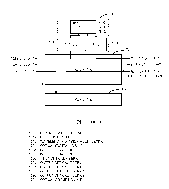
[0042] As shown in FIG 1, an optical switching device according to this
embodiment of the
present invention includes an optical switching unit 102, an optical grouping
unit 103, and a
service switching unit 101. This embodiment of the present invention is
illustrated with
multi-granularity switching as the background.
[0043] The optical switching unit 102 has optical input ports and optical
output ports,
where a part of the optical output ports are connected to input ports of the
optical grouping
unit 103.
[0044] The optical grouping unit 103 has the optical input ports and optical
output ports,
where the optical input ports of the optical grouping unit 103 are connected
to the optical
output ports of the optical switching unit 102, and the optical output ports
of the optical
6
CA 02744111 2011-05-18
grouping unit 103 are connected to the optical input ports of the optical
switching unit 102.
[0045] The optical switching unit 102 is configured to control transmission
paths of optical
signals. For example, as shown in FIGs. 2a and 2b, an optical switching unit
102a has the
function of inputting and outputting over a random port; and an optical
switching unit 102b
has the function of inputting over multiple ports and outputting over one
port. The optical
grouping unit 103 is configured to group the optical signals. For example, as
shown in FIG
2c, an optical grouping unit 103a has the function of randomly grouping and
outputting
input optical fiber wavelengths. It can be understood that, the function of
inputting over
multiple ports and outputting over one port in FIG. 2b may also be realized by
the optical
grouping unit 103a; the specific implementation is inputting the optical
signals over
multiple ports, and outputting the optical signals from the same output port
when the optical
signals are grouped (the path of the optical signals is in a reverse direction
of the path
shown in FIG 2c). Lines without an arrow in FIGs. 2a and 2b represent input
ports or
output ports, while lines with an arrow represent the transmission traces of
the light.
[0046] Hereinafter, this embodiment of the present invention is described with
several
common implementation schemes of granularity switching.
[0047] Optical fiber switching: An input optical fiber may be directly output
from any port
through the optical switching unit 102, as shown by the trace of an optical
fiber B in FIG 1
[0048] The optical fiber switching flow is: input optical fiber B -> optical
switching unit
102 -> output optical fiber B
[0049] Wavelength grouping and wavelength switching: Wavelengths in the input
optical
fiber may be randomly grouped through the optical grouping unit 103; as shown
in FIG 1,
the wavelengths of an input optical fiber C are grouped into groups CI and C2,
which are
output from ports 03 and 04 respectively, that is, output from an output
optical fiber C1
and an output optical fiber C2 respectively.
[0050] The wavelength grouping and wavelength switching flow is as follows:
7
CA 02744111 2011-05-18
-*
Input optical fiber C --~ optical switching unit -> optical grouping unit
Group Cl -> optical switching unit output port 03
Group C2 -* optical switching unit --- output port 04
[0051] Sub-wavelength switching: After service switching is performed on the
wavelengths
in the input optical fiber through electrical cross-connect (EXC), the
wavelengths are
loaded into other random optical fibers. As shown in FIG. 1, the wavelengths
in an input
optical fiber A pass through the service switching unit 101, where the service
switching unit
may be formed of wavelength division multiplexing (WDM)-EXC-WDM, the
wavelengths
in the input optical fiber A are output from 01 after service switching by the
WDM-EXC-WDM, and definitely, the wavelengths may also be loaded into other
groups
for outputting.
[0052] The sub-wavelength switching flow is as follows:
Input optical fiber A4optical switching unit- WDM- EXC- WDM4optical switching
unit-output port
Service switching
[0053] It can be known from the solution that, the device may only include the
optical
grouping unit 103 and the optical switching unit 102.
[0054] The optical switching unit 102 may be a strictly non-blocking optical
switch, and
may have a single-level structure or a cascade structure, for example, a three-
dimensional
micro electromechanical system (3D MEMS) single-level structure. The optical
grouping
unit 103 can realize any wavelength combination, and may include WSSs, where
the
number of the WSSs is determined by the maximum number of the switching
dimensions
of network nodes made up by the optical switching structure in the network,
and the scale
of the optical switching unit 102 may be a sum of the number of the input
optical fibers and
the number of the switching dimensions at peak times. This embodiment of the
present
invention does not limit the specific forms of the optical switching unit 102
and the optical
grouping unit 103, which does not affect the implementation of this
embodiment.
[0055] The optical fiber switching may be directly performed by the optical
switching unit
102; the wavelength grouping and wavelength switching is implemented after
grouping
8
CA 02744111 2011-05-18
with the optical grouping unit 103; and as the wavelengths are combined
according to
requirements, the demand for the switch matrix is reduced. It is assumed that
9 input optical
fibers (F 1, F2, ..., F9) are provided, where the input optical fiber F 1
needs to be grouped
into 8 groups at time Ti, F2 needs to be grouped into 5 groups at time Ti, and
F3 to F9
need to be directly connected in series. As the F1 needs to be grouped into 5
groups at time
T2, and F2 needs to be grouped into 8 groups at time T2, grouping resources
occupied by
the optical fiber F 1 can be released to the optical fiber F2 for sharing. If
the 9 optical fibers
need to be grouped into 40 groups in total at the peak time, only 49 x 49
switching units are
needed. However, in industrial solutions, F 1 to F9 are connected to an
optical switching
matrix after DEMUX, and with 80 waves per optical fiber as an example, the
scale of the
required switching units is 720 x 720. It can be seen that, the solution of
the present
invention can significantly reduce the scale requirement for the optical
switching unit 102.
[0056] Due to the flexibility of internal connection within optical switches,
the output of
the WSS may be sent to the next-level WSS, so as to realize flexible
combination of the
WSSs, and implement switching of different dimensions.
Embodiment 2
[0057] An embodiment of the present invention further provides an optical
switching
device. This embodiment of the present invention is illustrated with sharing
of an optical
grouping unit as the background.
[0058] As shown in FIG. 3a, the device may include an optical switching unit
302 and an
optical grouping unit 303. The extension of the dimension is realized through
sharing of an
optical grouping sub-unit. It is assumed that at time Ti, an optical fiber A
is required to
output 9 dimensions, and an optical fiber B is required to output 17
dimensions. As shown
in FIG. 3b, at time T2, the optical fiber A is required to output 17
dimensions, and the
optical fiber B is required to output 9 dimensions. As shown in FIG. 3c, at
time T3, the
optical fiber A is required to output 7 dimensions, the optical fiber B is
required to output 6
9
CA 02744111 2011-05-18
dimensions, and the optical fiber A7 and the optical fiber B6 need to be
combined into 1
dimension.
[0059] In this embodiment, the optical switching unit may be formed of 3D MEMS
large-scaled optical switches, and the optical grouping unit may include
optical grouping
sub-units. It is assumed that the optical grouping sub-unit has the function
of 1 port for
inputting and 9 dimensions for outputting, and it can be understood that the
number of the
input ports and the number of the output ports may also be other values, which
may not be
regarded as a limitation to the present invention.
[0060] At time Ti, the input optical fiber A is input to an optical grouping
sub-unit 3 in the
optical grouping unit through the optical switching unit, forming 9-dimension
outputting;
and similarly, the input optical fiber B forms 17-dimension outputting through
optical
grouping sub-units 1 and 2.
[0061] The connection relations at time Ti are as follows:
Input optical fiber A > optical switching unit > optical grouping sub-unit
3 > optical switching unit > output optical fiber
Input optical fiber B > optical switching unit > optical grouping sub-unit
1 >
> optical switching unit > output optical fiber
L > optical grouping sub unit 2 > optical switching unit > output optical
fiber
[0062] At time T2, the number of the output dimensions of the input optical
fiber A
changes to 17, and the number of the output dimensions of the input optical
fiber B changes
to 9. This change may be implemented by switching the connections between the
input
optical fibers A and B of the optical switching unit and the optical grouping
sub-units.
[0063] The connection relations at time T2 are as follows:
CA 02744111 2011-05-18
Input optical fiber B > optical switching unit > optical grouping sub-unit
3 > optical switching unit > output optical fiber
Input optical fiber A > optical switching unit > optical grouping sub-unit 1
{ > optical switching unit > output optical fiber
> optical grouping sub unit 2 > optical switching unit > output optical
fiber
[00641 At time T3, the number of the output dimensions of the input optical
fiber A
changes to 7, and the number of the output dimensions of the input optical
fiber B changes
to 6, where A7 and B6 are combined into 1 dimension. The total output
dimensions of the
optical fibers A and B are 12.
Input optical fiber A > optical switching unit > optical grouping sub-unit
I > optical switching unit
> optical switching unit > output optical fiber
> optical grouping sub-unit 3 > optical switching unit > output optical
fiber
Input optical fiber B > optical switching unit > optical grouping sub-unit
2 > optical switching unit
5 > optical switching unit > output optical fiber
>
optical grouping sub-unit 3 > optical switching unit > output optical
fiber
[00651 Furthermore, when the number of the output dimensions changes, the
optical
grouping unit may release idle optical grouping units, achieving the purpose
of saving the
optical grouping sub-units
[00661 The optical grouping sub-units directly transmit the optical signals
that need to be
re-grouped to other optical grouping sub-units, which is implemented in the
following
manner: The optical grouping unit is formed of optical grouping sub-units,
including a first
11
CA 02744111 2011-05-18
optical grouping sub-unit, a second optical grouping sub-unit, and a third
optical grouping
sub-unit.
[0067] Input ports of the first optical grouping sub-unit are connected to
output ports of the
optical switching unit, a part of output ports of the first optical grouping
sub-unit are
connected to input ports of the third optical grouping sub-unit, and a part of
output ports of
the first optical grouping sub-unit are connected to input ports of the
optical switching unit.
[0068] The input ports of the third optical grouping sub-unit are connected to
the output
ports of the first optical grouping sub-unit, a part of output ports of the
third optical
grouping sub-unit are connected to input ports of the second optical grouping
sub-unit, and
a part of output ports of the third optical grouping sub-unit are connected to
the input ports
of the optical switching unit.
[0069] The input ports of the second optical grouping sub-unit are connected
to the output
ports of the third optical grouping sub-unit, and output ports of the second
optical grouping
sub-unit are connected to the input ports of the optical switching unit.
[0070] In the embodiment, the optical switching process is completed by
grouping the
optical signals with the optical grouping unit and then switching the optical
signals with the
optical switching unit, and as the optical signals are combined according to
requirements,
the demand for the switch matrix is reduced, saving ports of the optical
switching unit.
Furthermore, optical grouping sub-units are saved through sharing the optical
grouping
sub-units.
Embodiment 3
[0071] An embodiment of the present invention provides an optical switching
device. This
embodiment of the present invention is illustrated with dimension extension as
the
background.
12
CA 02744111 2011-05-18
[0072] As shown in FIG. 4a, the device includes an optical switching unit 402
and an
optical grouping unit 403.
[0073] In this embodiment, wavelengths of the input optical fiber B are
initially grouped
into groups B 1 and B2. Now, it is assumed that the wavelengths of the input
optical fiber B
need to be grouped into n groups, the input optical fiber B is input to the
optical grouping
unit 403 through the optical switching unit 402, and the optical grouping unit
403 groups
the wavelengths into n groups and then sends the grouped wavelengths to the
optical
switching unit 402, so that the optical grouping unit 403 can output the n
groups to any
output ports, realizing the output grouping and extension. The extension of
the optical
grouping unit 403 is implemented by extending optical grouping sub-units.
[0074] The specific flow is as follows:
Bi 1B1'
Initial groups Groups after extension B2'
B2
Bn
[0075] The switching flow is as follows:
Group B 1' - optical switching unit 4 output port 02
Input optical fiber B--)optical grouping unit Group B2' - optical switching
unit -4 output port 03
Group Bn' - optical switching unit - output port On
[0076] Furthermore, switching dimensions may also be extended by the optical
grouping
sub-units. It is assumed that, at time T1, the input optical fiber B is
required to output 9
dimensions, and at time T2, the input optical fiber B is required to output 17
dimensions.
[0077] At time Ti, referring to FIG. 4a, the difference lies in that the
number of the
13
CA 02744111 2011-05-18
dimensions of the output optical fiber is 9 instead of n; the input optical
fiber B is required
to output 9 dimensions, and the requirement is realized by the grouping sub-
unit 1, that is,
the input optical fiber is input to the grouping sub-unit 1 through the
optical switching unit
402, and the grouping sub-unit 1 groups the input optical fiber into 9 groups
and then sends
the grouped optical fibers to the optical switching unit 402 for outputting.
At time T2, as
shown in FIG. 4b, the optical grouping unit 403 is formed of optical grouping
sub-units.
The number of the output dimension of the input optical fiber B is changed to
17, which is
realized by adding one level of the optical grouping sub-unit 2. The first-
level optical
grouping sub-unit 1 is re-grouped, where one group of output is sent to the
optical
switching unit 402 and input to the second-level optical grouping sub-unit 2,
and the optical
grouping sub-unit 2 groups the wavelengths and sends the grouped wavelengths
to the
optical switching unit 402 for realizing 17-dimension outputting.
[00781 In the embodiment, the optical switching process is completed by
grouping with the
optical signals the optical grouping unit and then switching the optical
signals with the
optical switching unit, and as the optical signals are combined according to
requirements,
the demand for the switch matrix is reduced, saving ports of the optical
switching unit.
Embodiment 4
[00791 An embodiment of the present invention further provides an optical
switching
device. This embodiment of the present invention is illustrated with
wavelength dispatching
as the background.
[0080] As shown in FIG. 5, the device includes an optical switching unit 502,
an optical
grouping unit 503, and a service switching unit 501. It is assumed that the
wavelengths Xl,
X2, k3, and a,4 in an input optical fiber B are required to be switched to an
optical fiber A.
[0081] The dispatching process may be: The input optical fiber B is switched
to the optical
grouping unit 503 through the optical switching unit 502, and the optical
grouping unit 503
14
CA 02744111 2011-05-18
divides the wavelengths in the optical fiber B into two groups, that is, B 1
(XI, X2, X3, and
k4) and B2 ()5, ..., k80) and sends the grouped wavelengths to the optical
switching unit
502; the optical switching unit 502 groups B, and switches B1 (X1, k2, k3, and
k4) to an
output port 01 together with the input optical fiber A, switching the
wavelengths O,l, k2,
X3, and k4) to the optical fiber A. The other group B2 (X5, ..., k80) is
output through other
ports according to requirements.
[0082] In the embodiment, the optical switching process is completed by
grouping optical
signals with the optical grouping unit and switching the optical signals with
the optical
switching unit, and as the optical signals are combined according to
requirements, the
demand for the switch matrix is reduced, saving ports of the optical switching
unit.
[0083] Persons of ordinary skill in the art should understand that all or a
part of the steps of
the method according to the embodiments of the present invention may be
implemented by
a program instructing relevant hardware. The program may be stored in a
computer
readable storage medium. The storage medium may be a read only memory (ROM), a
magnetic disk, or a compact disk.
[0084] The method and the device for optical switching provided in the
embodiments of the
present invention are described in detail above. The principle and
implementation of the
present invention are described herein through specific examples. The
description about the
embodiments of the present invention is merely provided for ease of
understanding of the
method and core ideas of the present invention. Persons of ordinary skill in
the art can make
variations and modifications to the present invention in terms of the specific
implementations and application scopes according to the ideas of the present
invention.
Therefore, the specification shall not be construed as a limitation to the
present invention.